EP0033495B1 - Verfahren zur Herstellung eines bipolaren Transistors mit hoher Geschwindigkeit - Google Patents
Verfahren zur Herstellung eines bipolaren Transistors mit hoher Geschwindigkeit Download PDFInfo
- Publication number
- EP0033495B1 EP0033495B1 EP81100495A EP81100495A EP0033495B1 EP 0033495 B1 EP0033495 B1 EP 0033495B1 EP 81100495 A EP81100495 A EP 81100495A EP 81100495 A EP81100495 A EP 81100495A EP 0033495 B1 EP0033495 B1 EP 0033495B1
- Authority
- EP
- European Patent Office
- Prior art keywords
- silicon
- layer
- emitter
- deposited
- window
- Prior art date
- Legal status (The legal status is an assumption and is not a legal conclusion. Google has not performed a legal analysis and makes no representation as to the accuracy of the status listed.)
- Expired
Links
Images


Classifications
-
- H—ELECTRICITY
- H10—SEMICONDUCTOR DEVICES; ELECTRIC SOLID-STATE DEVICES NOT OTHERWISE PROVIDED FOR
- H10W—GENERIC PACKAGES, INTERCONNECTIONS, CONNECTORS OR OTHER CONSTRUCTIONAL DETAILS OF DEVICES COVERED BY CLASS H10
- H10W20/00—Interconnections in chips, wafers or substrates
- H10W20/01—Manufacture or treatment
- H10W20/031—Manufacture or treatment of conductive parts of the interconnections
- H10W20/069—Manufacture or treatment of conductive parts of the interconnections by forming self-aligned vias or self-aligned contact plugs
-
- H—ELECTRICITY
- H10—SEMICONDUCTOR DEVICES; ELECTRIC SOLID-STATE DEVICES NOT OTHERWISE PROVIDED FOR
- H10D—INORGANIC ELECTRIC SEMICONDUCTOR DEVICES
- H10D10/00—Bipolar junction transistors [BJT]
- H10D10/01—Manufacture or treatment
- H10D10/051—Manufacture or treatment of vertical BJTs
-
- H—ELECTRICITY
- H10—SEMICONDUCTOR DEVICES; ELECTRIC SOLID-STATE DEVICES NOT OTHERWISE PROVIDED FOR
- H10D—INORGANIC ELECTRIC SEMICONDUCTOR DEVICES
- H10D62/00—Semiconductor bodies, or regions thereof, of devices having potential barriers
- H10D62/40—Crystalline structures
-
- H—ELECTRICITY
- H10—SEMICONDUCTOR DEVICES; ELECTRIC SOLID-STATE DEVICES NOT OTHERWISE PROVIDED FOR
- H10D—INORGANIC ELECTRIC SEMICONDUCTOR DEVICES
- H10D62/00—Semiconductor bodies, or regions thereof, of devices having potential barriers
- H10D62/80—Semiconductor bodies, or regions thereof, of devices having potential barriers characterised by the materials
- H10D62/83—Semiconductor bodies, or regions thereof, of devices having potential barriers characterised by the materials being Group IV materials, e.g. B-doped Si or undoped Ge
-
- H—ELECTRICITY
- H10—SEMICONDUCTOR DEVICES; ELECTRIC SOLID-STATE DEVICES NOT OTHERWISE PROVIDED FOR
- H10D—INORGANIC ELECTRIC SEMICONDUCTOR DEVICES
- H10D64/00—Electrodes of devices having potential barriers
- H10D64/60—Electrodes characterised by their materials
- H10D64/62—Electrodes ohmically coupled to a semiconductor
-
- H—ELECTRICITY
- H10—SEMICONDUCTOR DEVICES; ELECTRIC SOLID-STATE DEVICES NOT OTHERWISE PROVIDED FOR
- H10P—GENERIC PROCESSES OR APPARATUS FOR THE MANUFACTURE OR TREATMENT OF DEVICES COVERED BY CLASS H10
- H10P32/00—Diffusion of dopants within, into or out of wafers, substrates or parts of devices
- H10P32/10—Diffusion of dopants within, into or out of semiconductor bodies or layers
- H10P32/14—Diffusion of dopants within, into or out of semiconductor bodies or layers within a single semiconductor body or layer in a solid phase; between different semiconductor bodies or layers, both in a solid phase
- H10P32/1408—Diffusion of dopants within, into or out of semiconductor bodies or layers within a single semiconductor body or layer in a solid phase; between different semiconductor bodies or layers, both in a solid phase from or through or into an external applied layer, e.g. photoresist or nitride layers
- H10P32/1414—Diffusion of dopants within, into or out of semiconductor bodies or layers within a single semiconductor body or layer in a solid phase; between different semiconductor bodies or layers, both in a solid phase from or through or into an external applied layer, e.g. photoresist or nitride layers the applied layer being silicon, silicide or SIPOS, e.g. polysilicon or porous silicon
-
- H—ELECTRICITY
- H10—SEMICONDUCTOR DEVICES; ELECTRIC SOLID-STATE DEVICES NOT OTHERWISE PROVIDED FOR
- H10P—GENERIC PROCESSES OR APPARATUS FOR THE MANUFACTURE OR TREATMENT OF DEVICES COVERED BY CLASS H10
- H10P32/00—Diffusion of dopants within, into or out of wafers, substrates or parts of devices
- H10P32/10—Diffusion of dopants within, into or out of semiconductor bodies or layers
- H10P32/17—Diffusion of dopants within, into or out of semiconductor bodies or layers characterised by the semiconductor material
- H10P32/171—Diffusion of dopants within, into or out of semiconductor bodies or layers characterised by the semiconductor material being group IV material
-
- Y—GENERAL TAGGING OF NEW TECHNOLOGICAL DEVELOPMENTS; GENERAL TAGGING OF CROSS-SECTIONAL TECHNOLOGIES SPANNING OVER SEVERAL SECTIONS OF THE IPC; TECHNICAL SUBJECTS COVERED BY FORMER USPC CROSS-REFERENCE ART COLLECTIONS [XRACs] AND DIGESTS
- Y10—TECHNICAL SUBJECTS COVERED BY FORMER USPC
- Y10S—TECHNICAL SUBJECTS COVERED BY FORMER USPC CROSS-REFERENCE ART COLLECTIONS [XRACs] AND DIGESTS
- Y10S438/00—Semiconductor device manufacturing: process
- Y10S438/914—Doping
- Y10S438/92—Controlling diffusion profile by oxidation
-
- Y—GENERAL TAGGING OF NEW TECHNOLOGICAL DEVELOPMENTS; GENERAL TAGGING OF CROSS-SECTIONAL TECHNOLOGIES SPANNING OVER SEVERAL SECTIONS OF THE IPC; TECHNICAL SUBJECTS COVERED BY FORMER USPC CROSS-REFERENCE ART COLLECTIONS [XRACs] AND DIGESTS
- Y10—TECHNICAL SUBJECTS COVERED BY FORMER USPC
- Y10T—TECHNICAL SUBJECTS COVERED BY FORMER US CLASSIFICATION
- Y10T29/00—Metal working
- Y10T29/53—Means to assemble or disassemble
- Y10T29/53909—Means comprising hand manipulatable tool
- Y10T29/53943—Hand gripper for direct push or pull
Definitions
- the invention relates to a process for fabricating a high speed bipolar transistor in a semiconductor substrate where an emitter window is formed in an insulating layer deposited on said semiconductor substrate, where said window is filled by deposition with silicon of polycrystalline or amorphous structure, where ions are implanted into said silicon in said window, with said ions producing a conductivity type opposite to said of the substrate region underneath the window.
- ion implantation is defined as a process in which a beam of energetic particles is directed against a body of materials to selectively affect electrical and/or chemical changes in the body by the causing of the ions, of the beam, to pass into the body of the treated material.
- Ion implantation of impurities into semiconductor substrates has a number of significant advantages in the fabrication of semiconductor devices over the more conventional introduction by thermal diffusion. Since ion implantation is not a high temperature process, a larger number of materials, including organic photoresists, can be used as masking for controlling the area of implantation into the substrate. Also, multiple impurity introduction operations can be achieved without resort to high temperatures. Exposure to high temperatures, as in thermal diffusion, disperses the impurities previously introduced. Ion implantation techniques permit greater control of the placement and depth of penetration into the semiconductor. In general, the total amounts of impurities introduced and the depths of penetration can be more closely controlled by ion implantation techniques than with thermal diffusion from conventional sources.
- integrated circuit devices can be made smaller, with greater precision, with better control of heating, and with higher operating speeds using ion implantation technology.
- improvements in lithography permit smaller horizontal geometries the vertical dimensions of the semiconductor devices must also be compressed in order to achieve the highest performance.
- the emitter junction becomes very shallow (e.g. _200 nm) one experiences problems with junction passivation.
- One facet of the ion implantation process is that the ions are implanted a finite distance into the silicon. Although there is also some lateral scattering under the mask edge, this is much smaller than the vertical penetration. Hence the vertical junction depth will always be greater than the horizontal displacement under the mask edge. Clearly the ratio of horizontal to vertical displacement becomes smaller as the junction becomes shallower, at least for the same implant conditions. Too small of a lateral extent of the emitter under the insulator results in a poorly passivated or shorted emitter-base junction.
- a conventional technology employs a layer of Si 3 N 4 on top of a layer of Si0 2 for the purposes of passivation and self alignment.
- the opening in the top insulating layer serves as an etch mask for the lower Si0 2 layer.
- the emitter dopant is supplied by a low energy (20 to 50 Kev.) arsenic implant
- the upper insulator usually Si 3 N 4
- the oxide must be grown (150-200 A) in order to prevent outdiffusion of the arsenic.
- the conventional methods of contacting the emitter region enhance the difficulty of passivating very shallow structures.
- a silicide contact layer such as PtSi or Pd 2 Si. These are formed by interacting the precious metal with the silicon.
- the boundary between the silicide and the silicon is even closer to the perimeter of the emitter base junction.
- platinum silicide as a contact and/ or interconnection to a silicon region in an integrated circuit device is well known in the art. See for example, U.S. Patent No. 3,777,364.
- U.S. Patent 4,063,967 describes a method for forming doped zones in a semiconductor substrate where ion implantation is used to dope a polycrystalline or amorphous silicon layer selectively deposited onto the semiconductor substrate and subsequently the doped silicon layer is used to dope the underlying semiconductor substrate area.
- the purpose of the procedure is to avoid lattice distortions due to high surface concentrations of the dopant and lattice disturbancies due to ion beam damage.
- the process of the patent is not intended for the application in forming high speed transistors having a shallow emitter.
- the indicated process steps forming the emitter region and a PtSi contact to this region produced high yield well passivated emitter base junctions even if the junction depth was of the order of only 100 nm. Therefore the process according to the invention is especially suitable for producing transistors with a very shallow emitter region.
- the usage of ion implantation for doping the silicon layer ensures the precise dopant control.
- One of the reasons to go to very shallow emitter structures is to reduce the minority carrier (holes in the case of an n-p-n transistor) storage and thus, improve the transient response. In shallow emitters where the minority carrier diffusion length is greater than the emitter depth, the minority charge storage is proportional to the emitter thickness.
- the amorphous silicon layer is to be removed since it effectively adds to the emitter thickness.
- the amorphous layer is consumed in two steps. The first is an oxidation step which consumes about half of the thickness, -25 nm, and also provides part or possibly all of the thermal drive-in to form the emitter region in the single crystal silicon.
- the oxide is removed by etching in a hydrofluoric acid solution.
- the remainder of the amorphous silicon is consumed by the formation of the PtSi contact.
- the platinum silicide silicon interface provides a high surface recombination velocity in order to deplete the density of holes injected in the emitter.
- the low hole density in the emitter region has a direct benefit of decreasing the switching delay due to hole storage in the emitter, and hence higher device performance.
- the deposited silicon is made n-doped the oxidation and PtSi formation both tend to cause "pile up" of the impurity, whereby the concentration of n-type impurity in the shallow emitter will be very high and will thus guarantee a very high recombination rate and reduce hole storage.
- the thin (approximately 50 nm) amorphous or polycrystalline silicon layer forms a buffer region in which the emitter dopant is implanted.
- the ion implantation damage is confined to a thin silicon layer or to the thin silicon layer and the interfacial region between the substrate and the thin silicon layer. Since the regions being damaged are consumed completely by the oxidation and the PtSi formation a problem encountered when conventional ion implantation techniques are applied in forming transistors with shallow emitters does not occur.
- Conventional ion implantation techniques cause lattice damage in the regions that form active device areas later on. This damage is annealed by a heat treatment. This heat treatment or anneal is conventionally made in the process step where the dopant is driven-in thermally to the proper depth. However this drive-in is too short for this anneal when shallow emitters are formed.
- a sputtering technique is employed to deposit amorphous silicon and a CVD process to deposit polysilicon in the emitter window.
- the sputtering process provides a conformal coating which fills any undercut region.
- the diffusion coefficient of the impurities in the sputtering layer is very high and hence they spread out to give a uniform diffusion source over the emitter opening. With such a source, the diffusion into the single crystal silicon extends to about the same distance in the horizontal as in the vertical direction. This ensures the greatest possible horizontal displacement of the junction under the passivating silicon dioxide layer. Since the silicon layer must be very thin (-50 nm) and is to be consumed in subsequent processing, the thickness should be carefully controlled. The sputtering process can give a high degree of uniformity and reproducibility of layer thickness.
- the layer is its intimate contact with the single crystal silicon.
- a thin oxide layer will impede, or if thick enough, block the impurity atoms from reaching the single crystal silicon.
- the sputtering process with its energetic ions tends to disrupt the surface and to provide a more intimate contact.
- the surface can be cleaned, in situ, by a reverse sputtering or ion milling technique.
- a chemical vapor deposited (CVD) polysilicon layer does not provide the advantages of thickness control or interface quality of the sputtering process. If CVD is to be used, the energy of the implanted ions is adjusted to damage the interfacial region in order to make it amorphous, which provides a more uniform diffusion source.
- CVD chemical vapor deposited
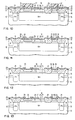
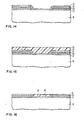
- FIGS 1 through 13 and 14 through 16 depict the structure at successive stages in the process in accordance with the invention.
- a monocrystalline silicon wafer 10 is oxidized forming a masking layer 11.
- a diffusion window 12 for forming the subcollector is made in the layer 11 using standard photolithographic and etching techniques.
- An N-type impurity is then introduced into wafer 10 forming the subcollector region 13.
- the impurity can be any suitable N-type impurity, as for example arsenic, and can be introduced into the wafer by any suitable technique, as e.g. capsule diffusion or ion implantation.
- the surface is re-oxidized forming the masking layer over the subcollector 13.
- Diffusion windows 14 are made for the annular sub-isolation region by standard photolithographic and subtractive etching techniques and a P-type impurity introduced to form the sub-isolation region 15.
- the impurity preferably is boron introduced by capsule diffusion or BBr3 diffusion.
- the masking layer 11 is removed and an epitaxial silicon layer 16 deposited on the surface of wafer 10.
- the epitaxial deposition process which is a high temperature process, the subcollector region 13 and the subisolation region 15 diffuses upwardly into the layer 16.
- the surface of the epitaxial layer 16 is oxidized in a suitable oxidizing atmosphere, as for example, steam at 950°C, forming thermal oxide layer 17.
- a layer 18 of Si 3 N 4 is subsequently deposited over layer 17 by conventional chemical vapor deposition (CVD) techniques that are well known in the industry.
- Si 3 N 4 layer 18 will serve as a mask to prevent oxidation of the underlying regions of the epitaxial layer during formation of the recessed oxidation isolation region which will be described hereafter.
- a layer of photoresist, not shown, is then deposited over the layer of CVD Si 3 N 4 . The resist is then exposed, developed to form windows which overlies the sub-isolation region 15.
- a second opening is also made which will result in an oxide region which separates the base region from the collector reach through region.
- photoresist as an etch mask, the exposed areas of the underlying Si 3 N 4 and Si0 2 layers are removed by reactive ion etching technique resulting in openings 19 which overlie the sub-isolation region 15 and opening 20 which overlies the region which will separate the collector reach through region from the base region of the transistor device.
- a portion of the epitaxial layer 16, that is exposed through windows 19 and 20 is removed by subtractive etching or reactive ion etching to a depth approximately 1/2 the depth that the recessed oxide region will extend into the epitaxial layer.
- the device is then exposed to an oxidizing atmosphere which results in the formation of the recessed oxide regions 21 on top of the sub-isolation region 15 and region 22 separating the collector reach through region from the base region.
- the oxidizing atmosphere is typically steam heated at 1000°C.
- the Si 3 N 4 layer 18 is removed and a layer of photoresist 23 deposited on the surface of the device.
- the resist layer 23 is exposed and developed to form an opening 24 which overlies the collector reach through region.
- a suitable N-type impurity, preferably phosphorus, is implanted into the epitaxial layer 16 to form collector reach through 25.
- phosphorus implantation is done at a high energy, as for example, 400 KeV, so as to make good reach through to the underlying subcollector 13.
- Resist layer 23 is then removed by using 0 2 plasma.
- a photoresist layer 26 is photolithographically patterned to expose the base area 27.
- a suitable P-type impurity preferably boron
- the implant energy and dose depend upon the thickness of the oxide layer and the desired vertical device geometry. For example, an implantation of 10 14 boron atoms at 50 KeV and a thickness of 100 nm of the oxide layer 17 is used to produce a base collector junction about 400 nm deep in a 0.3 ohm cm epi layer.
- the resist layer 26 is removed by an 0 2 plasma.
- a layer of Si 3 N 4 29 is deposited over the oxide layer 17.
- a layer of photoresist is deposited over layer 29. The photoresist layer is exposed and developed to produce a window 30 for the emitter contact, a window 31 for the base contact, and a window 32 for the collector contact.
- the silicon nitride layer 29 is removed in all of the device contact regions 30, 31 and 32.
- a photolithographic step is applied to form a block out mask to prevent etching of the oxide 17 in the base contact 31 while the oxide is etched from the emitter 30 and collector 32 contact regions. It is this step which can cause undercutting of the oxide layer 17 at the edges of the emitter and collector contact openings 30 and 32.
- an amorphous silicon 33 layer is deposited.
- the deposition should be conformal.
- the technique must also provide good thickness uniformity and reproducibility. These capabilities have been demonstrated by the sputtering methods.
- the thickness of the deposited silicon layer depends upon the desired vertical device dimensions, but, is typically in the 50 to 100 nm range.
- Doping of the amorphous silicon layer is then accomplished by a blanket ion implantation of arsenic.
- the energy and dose of the implanted arsenic ions is adjusted to confine the dopant to the deposited silicon layer. For example, with a 50 nm layer thickness an energy of 30 to 40 KeV with a dose of 2 x 10 11 atoms/cm 2 for a final emitter depth of 100 nm.
- the arsenic implanted amorphous silicon layer is oxidized 34 in order to consume approximately one-half of the layer thickness.
- the arsenic diffusion during this step.
- it should be accomplished at a low temperature, for example, 900°C.
- the oxidation step also provides an unpermeable cap which prevents the escape of the arsenic dopant from the amorphous silicon layer. Since the segregation coefficient favors the silicon side of the oxide interface, the arsenic impurities pile up in front of the advancing oxide silicon interface.
- a photo resist layer 37 is photolithographically defined to cover the emitter and collector regions. This is used as an etch mask to remove the oxide layer 34 on top of the polysilicon.
- the photoresist is removed and the oxide 34 remaining over the emitter and collector contacts is used as a mask to etch the amorphous silicon 33.
- the amorphous silicon etching can be accomplished by reactive ion or wet chemical etching.
- the oxide layer 17 over the base contact 31 is removed with a buffered HF solution. This etch step also removes the oxide 34 on top of the remaining amorphous silicon 33 over the emitter and collector contact.
- a layer of Pt is deposited on the wafer.
- the thickness of the Pt film is made to be approximately the same as the remaining amorphous silicon.
- the wafer is then heated to about 500°C in forming gas for about 30 minutes to react the platinum with the underlaying silicon to form PtSi.
- the unreacted Pt on top of the dielectric areas is then removed in an aqua regia solution leaving the PtSi contacts 38, 39 and 40 to the emitter, base, and collector of the transistor.
- the device illustrated in Figure 13 is now ready for the deposition and fabricating of the metallurgy system which will interconnect the device shown with other devices, resistors, and the like on the same substrate 10 into electrical circuits.
- the forming of the metallurgy system is well known in the art and will not be discussed or described. It will be understood that the preferred embodiment illustrated and described in Figures 1 through 13 is an NPN device. It is understood that the conductivity types could be reversed, the impurities changed and other modifications made without departing from the scope of the invention as defined by the appended claims.
- Figure 14 which depicts only the emitter or collector contact region, a layer of CVD Si0 2 41 is deposited on the silicon nitride. The contact openings are formed and the amorphous silicon 33 deposited as previously described.
- the wafer is reactive ion etched until the CVD Si0 2 layer 41 is reached.
- the reactive ion etch conditions must be adjusted to provide equal etch rates of the amorphous silicon and photoresist.
- Part or all of the CVD oxide 41 can be removed which gives a buffer to thickness variations.
- the residual photoresist 42 in the opening is removed with an O2 plasma.
- a blanket implant or an implant with a blockout mask of arsenic is performed as described above.
Landscapes
- Bipolar Transistors (AREA)
- Electrodes Of Semiconductors (AREA)
- Element Separation (AREA)
Claims (6)
Applications Claiming Priority (2)
| Application Number | Priority Date | Filing Date | Title |
|---|---|---|---|
| US117887 | 1980-02-01 | ||
| US06/117,887 US4301588A (en) | 1980-02-01 | 1980-02-01 | Consumable amorphous or polysilicon emitter process |
Publications (3)
| Publication Number | Publication Date |
|---|---|
| EP0033495A2 EP0033495A2 (de) | 1981-08-12 |
| EP0033495A3 EP0033495A3 (en) | 1982-09-01 |
| EP0033495B1 true EP0033495B1 (de) | 1986-04-16 |
Family
ID=22375352
Family Applications (1)
| Application Number | Title | Priority Date | Filing Date |
|---|---|---|---|
| EP81100495A Expired EP0033495B1 (de) | 1980-02-01 | 1981-01-23 | Verfahren zur Herstellung eines bipolaren Transistors mit hoher Geschwindigkeit |
Country Status (5)
| Country | Link |
|---|---|
| US (1) | US4301588A (de) |
| EP (1) | EP0033495B1 (de) |
| JP (1) | JPS56114352A (de) |
| CA (1) | CA1148273A (de) |
| DE (1) | DE3174374D1 (de) |
Families Citing this family (21)
| Publication number | Priority date | Publication date | Assignee | Title |
|---|---|---|---|---|
| US4452645A (en) * | 1979-11-13 | 1984-06-05 | International Business Machines Corporation | Method of making emitter regions by implantation through a non-monocrystalline layer |
| JPS584924A (ja) * | 1981-07-01 | 1983-01-12 | Hitachi Ltd | 半導体装置の電極形成方法 |
| GB8507624D0 (en) * | 1985-03-23 | 1985-05-01 | Standard Telephones Cables Ltd | Semiconductor devices |
| KR890004973B1 (ko) * | 1985-04-10 | 1989-12-02 | 후지쓰 가부시기 가이샤 | 자기정합된 바이폴라트랜지스터의 제조방법 |
| GB2186423A (en) * | 1985-11-29 | 1987-08-12 | Plessey Co Plc | Integrated circuit transistor and method for producing same |
| KR910005401B1 (ko) * | 1988-09-07 | 1991-07-29 | 경상현 | 비결정 실리콘을 이용한 자기정렬 트랜지스터 제조방법 |
| KR930004720B1 (ko) * | 1988-11-04 | 1993-06-03 | 마쯔시따 덴끼 산교 가부시끼가이샤 | 반도체장치 및 그 제조방법 |
| US5318917A (en) * | 1988-11-04 | 1994-06-07 | Matsushita Electric Industrial Co., Ltd. | Method of fabricating semiconductor device |
| US5204274A (en) * | 1988-11-04 | 1993-04-20 | Matsushita Electric Industrial Co., Ltd. | Method of fabricating semiconductor device |
| GB2238658B (en) * | 1989-11-23 | 1993-02-17 | Stc Plc | Improvements in integrated circuits |
| US5366917A (en) * | 1990-03-20 | 1994-11-22 | Nec Corporation | Method for fabricating polycrystalline silicon having micro roughness on the surface |
| US5691249A (en) * | 1990-03-20 | 1997-11-25 | Nec Corporation | Method for fabricating polycrystalline silicon having micro roughness on the surface |
| US5488003A (en) * | 1993-03-31 | 1996-01-30 | Intel Corporation | Method of making emitter trench BiCMOS using integrated dual layer emitter mask |
| US5670394A (en) * | 1994-10-03 | 1997-09-23 | United Technologies Corporation | Method of making bipolar transistor having amorphous silicon contact as emitter diffusion source |
| US6015740A (en) * | 1997-02-10 | 2000-01-18 | Advanced Micro Devices, Inc. | Method of fabricating CMOS devices with ultra-shallow junctions and reduced drain area |
| SE512813C2 (sv) | 1997-05-23 | 2000-05-15 | Ericsson Telefon Ab L M | Förfarande för framställning av en integrerad krets innefattande en dislokationsfri kollektorplugg förbunden med en begravd kollektor i en halvledarkomponent, som är omgiven av en dislokationsfri trench samt integrerad krets framställd enligt förfarandet |
| US6153456A (en) * | 1998-01-14 | 2000-11-28 | Vlsi Technology, Inc. | Method of selectively applying dopants to an integrated circuit semiconductor device without using a mask |
| US6773973B2 (en) * | 2001-08-13 | 2004-08-10 | Maxim Integrated Products, Inc. | Semiconductor transistor having a polysilicon emitter and methods of making the same |
| US9925678B2 (en) | 2014-12-30 | 2018-03-27 | The Gillette Company Llc | Razor blade with a printed object |
| US10384360B2 (en) | 2016-06-29 | 2019-08-20 | The Gillette Company Llc | Razor blade with a printed object |
| US10675772B2 (en) * | 2016-06-29 | 2020-06-09 | The Gillette Company Llc | Printed lubricious material disposed on razor blades |
Family Cites Families (11)
| Publication number | Priority date | Publication date | Assignee | Title |
|---|---|---|---|---|
| US3558366A (en) * | 1968-09-17 | 1971-01-26 | Bell Telephone Labor Inc | Metal shielding for ion implanted semiconductor device |
| US3777364A (en) * | 1972-07-31 | 1973-12-11 | Fairchild Camera Instr Co | Methods for forming metal/metal silicide semiconductor device interconnect system |
| DE2449688C3 (de) * | 1974-10-18 | 1980-07-10 | Siemens Ag, 1000 Berlin Und 8000 Muenchen | Verfahren zur Herstellung einer dotierten Zone eines Leitfähigkeitstyps in einem Halbleiterkörper |
| JPS5928992B2 (ja) * | 1975-02-14 | 1984-07-17 | 日本電信電話株式会社 | Mosトランジスタおよびその製造方法 |
| US4011105A (en) * | 1975-09-15 | 1977-03-08 | Mos Technology, Inc. | Field inversion control for n-channel device integrated circuits |
| NL7604445A (nl) * | 1976-04-27 | 1977-10-31 | Philips Nv | Werkwijze ter vervaardiging van een halfgelei- derinrichting, en inrichting vervaardigd door toepassing van de werkwijze. |
| DE2627855A1 (de) * | 1976-06-22 | 1977-12-29 | Siemens Ag | Halbleiterbauelement mit wenigstens zwei, einen pn-uebergang bildenden zonen unterschiedlichen leitungstyps sowie verfahren zu dessen herstellung |
| JPS53129981A (en) * | 1977-04-19 | 1978-11-13 | Fujitsu Ltd | Production of semiconductor device |
| US4109372A (en) * | 1977-05-02 | 1978-08-29 | International Business Machines Corporation | Method for making an insulated gate field effect transistor utilizing a silicon gate and silicide interconnection vias |
| US4190466A (en) * | 1977-12-22 | 1980-02-26 | International Business Machines Corporation | Method for making a bipolar transistor structure utilizing self-passivating diffusion sources |
| US4242791A (en) * | 1979-09-21 | 1981-01-06 | International Business Machines Corporation | High performance bipolar transistors fabricated by post emitter base implantation process |
-
1980
- 1980-02-01 US US06/117,887 patent/US4301588A/en not_active Expired - Lifetime
- 1980-12-17 CA CA000366999A patent/CA1148273A/en not_active Expired
-
1981
- 1981-01-09 JP JP130481A patent/JPS56114352A/ja active Pending
- 1981-01-23 EP EP81100495A patent/EP0033495B1/de not_active Expired
- 1981-01-23 DE DE8181100495T patent/DE3174374D1/de not_active Expired
Also Published As
| Publication number | Publication date |
|---|---|
| EP0033495A3 (en) | 1982-09-01 |
| EP0033495A2 (de) | 1981-08-12 |
| CA1148273A (en) | 1983-06-14 |
| US4301588A (en) | 1981-11-24 |
| JPS56114352A (en) | 1981-09-08 |
| DE3174374D1 (en) | 1986-05-22 |
Similar Documents
| Publication | Publication Date | Title |
|---|---|---|
| US4301588A (en) | Consumable amorphous or polysilicon emitter process | |
| EP0137645B1 (de) | Verfahren zur Bildung eines seichten Gebietes des N-Typs | |
| US4481706A (en) | Process for manufacturing integrated bi-polar transistors of very small dimensions | |
| US5166767A (en) | Sidewall contact bipolar transistor with controlled lateral spread of selectively grown epitaxial layer | |
| EP0265489B1 (de) | Verfahren zur herstellung von halbleiterbauelementen | |
| EP0188291B1 (de) | Bipolare Halbleiteranordnung und Verfahren zu ihrer Herstellung | |
| US4711017A (en) | Formation of buried diffusion devices | |
| US4418469A (en) | Method of simultaneously forming buried resistors and bipolar transistors by ion implantation | |
| EP0314600B1 (de) | Selbstjustierter Polysiliziumemitter und Kontaktstruktur für Hochleistungsbipolartransistor | |
| US4354307A (en) | Method for mass producing miniature field effect transistors in high density LSI/VLSI chips | |
| EP0076106B1 (de) | Verfahren zur Herstellung eines bipolaren Transistors | |
| US5443994A (en) | Method of fabricating a semiconductor device having a borosilicate glass spacer | |
| US4660276A (en) | Method of making a MOS field effect transistor in an integrated circuit | |
| US5614422A (en) | Process for doping two levels of a double poly bipolar transistor after formation of second poly layer | |
| US6077744A (en) | Semiconductor trench MOS devices | |
| EP0287318B1 (de) | Integrierter Transistor und sein Herstellungsverfahren | |
| JPS6133253B2 (de) | ||
| EP0104079B1 (de) | Kontaktstruktur für integrierte Schaltung | |
| US4289550A (en) | Method of forming closely spaced device regions utilizing selective etching and diffusion | |
| EP0219243A2 (de) | Verfahren zur Herstellung eines bipolaren Transistors | |
| KR100495284B1 (ko) | 반도체장치의제조방법 | |
| JPS5947468B2 (ja) | バイポ−ラ・トランジスタの製造方法 | |
| JPH05190481A (ja) | 基板中のドープ領域製造方法 | |
| EP0042380B1 (de) | Verfahren zum erreichen eines idealen fremdstoffkonzentrationsverlaufs für die basiszone eines transistors | |
| JPH0648690B2 (ja) | 半導体装置の製造方法 |
Legal Events
| Date | Code | Title | Description |
|---|---|---|---|
| PUAI | Public reference made under article 153(3) epc to a published international application that has entered the european phase |
Free format text: ORIGINAL CODE: 0009012 |
|
| AK | Designated contracting states |
Designated state(s): DE FR GB IT |
|
| 17P | Request for examination filed |
Effective date: 19811030 |
|
| PUAL | Search report despatched |
Free format text: ORIGINAL CODE: 0009013 |
|
| AK | Designated contracting states |
Designated state(s): DE FR GB IT |
|
| GRAA | (expected) grant |
Free format text: ORIGINAL CODE: 0009210 |
|
| AK | Designated contracting states |
Kind code of ref document: B1 Designated state(s): DE FR GB IT |
|
| PG25 | Lapsed in a contracting state [announced via postgrant information from national office to epo] |
Ref country code: IT Free format text: LAPSE BECAUSE OF FAILURE TO SUBMIT A TRANSLATION OF THE DESCRIPTION OR TO PAY THE FEE WITHIN THE PRESCRIBED TIME-LIMIT;WARNING: LAPSES OF ITALIAN PATENTS WITH EFFECTIVE DATE BEFORE 2007 MAY HAVE OCCURRED AT ANY TIME BEFORE 2007. THE CORRECT EFFECTIVE DATE MAY BE DIFFERENT FROM THE ONE RECORDED. Effective date: 19860416 |
|
| REF | Corresponds to: |
Ref document number: 3174374 Country of ref document: DE Date of ref document: 19860522 |
|
| ET | Fr: translation filed | ||
| PLBE | No opposition filed within time limit |
Free format text: ORIGINAL CODE: 0009261 |
|
| STAA | Information on the status of an ep patent application or granted ep patent |
Free format text: STATUS: NO OPPOSITION FILED WITHIN TIME LIMIT |
|
| 26N | No opposition filed | ||
| PGFP | Annual fee paid to national office [announced via postgrant information from national office to epo] |
Ref country code: GB Payment date: 19901220 Year of fee payment: 11 |
|
| PGFP | Annual fee paid to national office [announced via postgrant information from national office to epo] |
Ref country code: DE Payment date: 19910131 Year of fee payment: 11 |
|
| PGFP | Annual fee paid to national office [announced via postgrant information from national office to epo] |
Ref country code: FR Payment date: 19911218 Year of fee payment: 12 |
|
| PG25 | Lapsed in a contracting state [announced via postgrant information from national office to epo] |
Ref country code: GB Effective date: 19920123 |
|
| REG | Reference to a national code |
Ref country code: GB Ref legal event code: PCNP |
|
| PG25 | Lapsed in a contracting state [announced via postgrant information from national office to epo] |
Ref country code: DE Effective date: 19921001 |
|
| PG25 | Lapsed in a contracting state [announced via postgrant information from national office to epo] |
Ref country code: FR Effective date: 19930930 |
|
| REG | Reference to a national code |
Ref country code: FR Ref legal event code: ST |