EP0034342A1 - Céramique piézo-électrique - Google Patents
Céramique piézo-électrique Download PDFInfo
- Publication number
- EP0034342A1 EP0034342A1 EP81100999A EP81100999A EP0034342A1 EP 0034342 A1 EP0034342 A1 EP 0034342A1 EP 81100999 A EP81100999 A EP 81100999A EP 81100999 A EP81100999 A EP 81100999A EP 0034342 A1 EP0034342 A1 EP 0034342A1
- Authority
- EP
- European Patent Office
- Prior art keywords
- coupling factor
- piezoelectric
- ratio
- oxide material
- thickness
- Prior art date
- Legal status (The legal status is an assumption and is not a legal conclusion. Google has not performed a legal analysis and makes no representation as to the accuracy of the status listed.)
- Granted
Links
- 239000000463 material Substances 0.000 title claims abstract description 48
- 238000010168 coupling process Methods 0.000 claims abstract description 49
- 238000005859 coupling reaction Methods 0.000 claims abstract description 49
- 230000008878 coupling Effects 0.000 claims abstract description 48
- 239000000203 mixture Substances 0.000 claims abstract description 12
- 239000000654 additive Substances 0.000 claims abstract description 7
- JEIPFZHSYJVQDO-UHFFFAOYSA-N iron(III) oxide Inorganic materials O=[Fe]O[Fe]=O JEIPFZHSYJVQDO-UHFFFAOYSA-N 0.000 claims abstract description 6
- 230000000996 additive effect Effects 0.000 claims abstract description 4
- 239000000523 sample Substances 0.000 abstract description 14
- 229910003781 PbTiO3 Inorganic materials 0.000 description 14
- 238000005245 sintering Methods 0.000 description 13
- 239000000919 ceramic Substances 0.000 description 8
- GNRSAWUEBMWBQH-UHFFFAOYSA-N nickel(II) oxide Inorganic materials [Ni]=O GNRSAWUEBMWBQH-UHFFFAOYSA-N 0.000 description 5
- 230000000052 comparative effect Effects 0.000 description 4
- 230000015556 catabolic process Effects 0.000 description 3
- 238000004519 manufacturing process Methods 0.000 description 3
- 239000000843 powder Substances 0.000 description 3
- GWEVSGVZZGPLCZ-UHFFFAOYSA-N Titan oxide Chemical compound O=[Ti]=O GWEVSGVZZGPLCZ-UHFFFAOYSA-N 0.000 description 2
- 230000003247 decreasing effect Effects 0.000 description 2
- 230000007547 defect Effects 0.000 description 2
- 230000000694 effects Effects 0.000 description 2
- 230000003631 expected effect Effects 0.000 description 2
- NUJOXMJBOLGQSY-UHFFFAOYSA-N manganese dioxide Chemical compound O=[Mn]=O NUJOXMJBOLGQSY-UHFFFAOYSA-N 0.000 description 2
- 238000000034 method Methods 0.000 description 2
- 239000002994 raw material Substances 0.000 description 2
- 229910019653 Mg1/3Nb2/3 Inorganic materials 0.000 description 1
- 239000004372 Polyvinyl alcohol Substances 0.000 description 1
- 230000002411 adverse Effects 0.000 description 1
- 230000003679 aging effect Effects 0.000 description 1
- 229910002056 binary alloy Inorganic materials 0.000 description 1
- 239000011230 binding agent Substances 0.000 description 1
- 229910000019 calcium carbonate Inorganic materials 0.000 description 1
- 150000004649 carbonic acid derivatives Chemical class 0.000 description 1
- 238000006243 chemical reaction Methods 0.000 description 1
- QDOXWKRWXJOMAK-UHFFFAOYSA-N chromium(III) oxide Inorganic materials O=[Cr]O[Cr]=O QDOXWKRWXJOMAK-UHFFFAOYSA-N 0.000 description 1
- IVMYJDGYRUAWML-UHFFFAOYSA-N cobalt(II) oxide Inorganic materials [Co]=O IVMYJDGYRUAWML-UHFFFAOYSA-N 0.000 description 1
- 230000005684 electric field Effects 0.000 description 1
- 238000010438 heat treatment Methods 0.000 description 1
- 150000004679 hydroxides Chemical class 0.000 description 1
- YEXPOXQUZXUXJW-UHFFFAOYSA-N lead(II) oxide Inorganic materials [Pb]=O YEXPOXQUZXUXJW-UHFFFAOYSA-N 0.000 description 1
- 229910000016 manganese(II) carbonate Inorganic materials 0.000 description 1
- 238000005259 measurement Methods 0.000 description 1
- 239000002184 metal Substances 0.000 description 1
- 229910052751 metal Inorganic materials 0.000 description 1
- 239000007769 metal material Substances 0.000 description 1
- 238000010310 metallurgical process Methods 0.000 description 1
- 150000003891 oxalate salts Chemical class 0.000 description 1
- 230000010287 polarization Effects 0.000 description 1
- 229920002451 polyvinyl alcohol Polymers 0.000 description 1
- 239000006104 solid solution Substances 0.000 description 1
- ZNOKGRXACCSDPY-UHFFFAOYSA-N tungsten(VI) oxide Inorganic materials O=[W](=O)=O ZNOKGRXACCSDPY-UHFFFAOYSA-N 0.000 description 1
- XLYOFNOQVPJJNP-UHFFFAOYSA-N water Substances O XLYOFNOQVPJJNP-UHFFFAOYSA-N 0.000 description 1
Images

Classifications
-
- H—ELECTRICITY
- H10—SEMICONDUCTOR DEVICES; ELECTRIC SOLID-STATE DEVICES NOT OTHERWISE PROVIDED FOR
- H10N—ELECTRIC SOLID-STATE DEVICES NOT OTHERWISE PROVIDED FOR
- H10N30/00—Piezoelectric or electrostrictive devices
- H10N30/80—Constructional details
- H10N30/85—Piezoelectric or electrostrictive active materials
- H10N30/853—Ceramic compositions
Definitions
- the present invention relates to a piezoelectric oxide material and, more particularly, to a PbTi0 3 type piezoelectric material suitable for ultrasonic probes.
- PbTi0 3 type materials having anisotropic coupling factors are reported. According to these materials, the value of thickness coupling factor Kt greatly differs from the planar coupling factor Kp of those materials.
- the sintered body is fragile due to cracks caused in sintering and therefore a large sintered body of over 20 mm diameter cannot be obtained.
- the poling (polarization) must be performed at severe conditions such as 60 kV/cm at 200°C. This tends to cause spark breakdown of samples and makes it difficult to obtain a large vibrator.
- the thickness coupling factor Kt is 40 to 48%, and the planar coupling factor Kp is above 8%.
- the ratio of the coupling factors Kt/Kp has been limited to 4 to 6, and spurious response due to overtones determined by the planar coupling factor Kp in the high frequency region have not been negligible.
- the present invention has been made to overcome these problems of the prior art and has for its object to provide a piezoelectric oxide material of which the thickness coupling factor Kt is as large as 50% or more; the planar coupling factor Kp is 3 to 5%; the ratio Kt/Kp is 10 to 19; the dielectric constant is as small as 300 or less; sintering is easy, allowing the production of large vibrators of over 50 cm diameter; and poling is easier than that of conventional PbTi0 3 materials.
- the present invention thus provides a piezoelectric oxide material comprising a basic composition having a general formula (Pb 1 - a Ca a )[(Co1 ⁇ 2W1 ⁇ 2 )xTi 1-X ]O 3 wherein 0.01 ⁇ x ⁇ 0.10 and 0.20 ⁇ a ⁇ 0.35, to which is added, as an additive, 0.05 to 2.0% by weight based on the basic composition of at least one of MnO, NiO and Fe 2 0 3 ; the thickness coupling factor (Kt) is 50% or more; and the ratio (Kt/Kp) of the thickness coupling factor (Kt) to the planar coupling factor (Kp) is 10 or more.
- a general formula (Pb 1 - a Ca a )[(Co1 ⁇ 2W1 ⁇ 2 )xTi 1-X ]O 3 wherein 0.01 ⁇ x ⁇ 0.10 and 0.20 ⁇ a ⁇ 0.35, to which is added, as an additive, 0.05 to 2.0% by weight
- the reason why the total content of MnO, NiO and Fe 2 0 3 is limited to 0.05 to 2.0% by weight relative to the total weight of the composition may be explained as follows. When it is less than 0.05% by weight, the expected effects of the additives, i.e., to improve the sintering and the poling characteristics of the PbTi0 3 ceramic, are not achieved. When it is more than 2.0%, the sintering of the ceramic becomes difficult.
- the preferred range of the additives is 0.5 to 1.0% by weight.
- the piezoelectric oxide material of the present invention of the type described above may be easily prepared by a conventional powder metallurgical process in general.
- the raw material oxides, PbO, TiO 2 , CaC0 3 , MnC0 3 , NiO, CoO, W0 3 , Fe 2 0 3 and so on are correctly weighed to a predetermined ratio and are mixed well in a ball mill or the like.
- the another raw materials which are converted to oxides upon heating for example, hydroxides, carbonates, oxalates may be employable.
- the mixture is then calcined at a temperature of about 600 to 900°C and is ground in a ball mill or the like to prepare a fine powder.
- a binder such as water and polyvinyl alcohol
- the compact is formed under a pressure of about 0.5 to 2 ton/cm 2 and is sintered at a temperature of about 1,100 to 1,200°C. Since one component of the composition, PbO, may partially evaporate during this sintering process, the sintering is performed in a closed furnace.
- the forming compact is usually held at maximum temperature for a period of 0.5 to 3 hours.
- the thickness coupling factor Kt is substantially equal to the planar coupling factor Kp. This results in the practical difficulty of spurious response due to overtones of the vibrations of the planar mode when preparing a vibrator utilizing vibrations in the direction of the thickness.
- the thickness coupling factor Kt is as large as 50% or more but the planar coupling factor Kp is as small as 3 to 5%, so that the spurious response at high frequency region are advantageously reduced to a negligible level.
- the sintering temperature may be reduced and the sintering characteristics of the PbTi0 3 type material may be improved so that large ceramic may be obtained.
- the sintering performance, the poling characteristics, and the ageing properties of the resonant frequency may be improved.
- the sintered sample is polished to a shapa of 20 (diameter) x 0.5 mm (thickness). Electrodes are formed on both surfaces of the sample. After poling it under the conditions of 100°C and 40 kV/cm, the piezoelectric characteristics were respectively measured by the standard circuit method disclosed in P roc. IRE. vol. 137 (1949), pp. 1,378 to 1,395. The results are shown in Table 1 together with the composition ratios of these sintered bodies.
- F.T. indicates the sintering temperature (°C); D, the density (at 23°C); ⁇ , the dielectric constant (at 1 kHz and 23°C); Kt, the thickness coupling factor (%); Kp, the planar coupling factor (%); and Kt/Kp the ratio of these coupling factors.
- the samples a, b, c, d, e, f, g and h correspond to Examples 9, 10, 11, 12, 13, 14, 15 and 16, and the samples i, j and k correspond to Comparative Examples 1, 3 and 4.
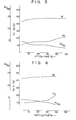
- the thickness coupling factor Kt is as large as 50% or more while the coupling factor Kp is as small as 3 to 5%, so that the coupling factor ratio Kt/Kp reaches 10 to 19 when 0.20 ⁇ a s 0.35.
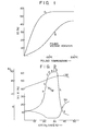
- Fig. 4 shows the coupling factors Kt and Kp, and their ratio Kt/Kp of the material in which Ba replaces part of the Pb in PbTiO 3 .
- Fig. 5 is a graph of the number of spurious response that is relative to the coupling factor ratio Kt/Kp.
- the ceramic vibrators whose resonant frequency are 2.25 MHz at the thickness extensional mode were prepared for the measurement.
- the number of spurious response were measured from 0.5 MHz to 3 MHz.
- the spurious responses plotted in the graph represent those having more than 0.5 dB in impedance difference between at the resonant frequency and the anti-resonant frequency.
- the spurious responses are progressively decreased in accordance with increase in the value of Kt/Kp ratio.
- the piezoelectric material of the present invention generates only a small degree of spurious response.
- the vibration element of an ultrasonic probe is formed of the material of the present invention, the input signal energy supplied to the probe is efficiently converted into the vertical mode ultrasonic wave.
- the piezoelectric material of the present invention permits producing a good efficient ultrasonic probe.
- the dielectric constant of the present invention is about 180 to 300, which is 1 ⁇ 3 to those of conventional piezoelectric materials. If the conventional materials may be used up to 10 MHz, the material of the present invention may be used up to 50 MHz.
- the larger and thinner sound conversion element is needed.
- a large dimensional thinner ceramics vibrator is hard to obtain with conventional PbTi0 3 type piezoelectric materials.
- a large and thinner ceramic vibrator e.g., 50 to 10 mm long, 15 to 20 mm wide, and 200 ⁇ m thick
- excellent mechanical strength may be easily obtained.
- the piezoelectric material of the present invention is applicable to fields to which conventional piezoelectric materials have not been applicable heretofore.
Landscapes
- Chemical & Material Sciences (AREA)
- Engineering & Computer Science (AREA)
- Ceramic Engineering (AREA)
- Compositions Of Oxide Ceramics (AREA)
- Inorganic Insulating Materials (AREA)
Applications Claiming Priority (2)
| Application Number | Priority Date | Filing Date | Title |
|---|---|---|---|
| JP17911/80 | 1980-02-18 | ||
| JP55017911A JPS6023512B2 (ja) | 1980-02-18 | 1980-02-18 | 酸化物圧電材料 |
Publications (2)
| Publication Number | Publication Date |
|---|---|
| EP0034342A1 true EP0034342A1 (fr) | 1981-08-26 |
| EP0034342B1 EP0034342B1 (fr) | 1983-10-05 |
Family
ID=11956926
Family Applications (1)
| Application Number | Title | Priority Date | Filing Date |
|---|---|---|---|
| EP81100999A Expired EP0034342B1 (fr) | 1980-02-18 | 1981-02-12 | Céramique piézo-électrique |
Country Status (4)
| Country | Link |
|---|---|
| US (1) | US4321155A (fr) |
| EP (1) | EP0034342B1 (fr) |
| JP (1) | JPS6023512B2 (fr) |
| DE (1) | DE3161068D1 (fr) |
Cited By (1)
| Publication number | Priority date | Publication date | Assignee | Title |
|---|---|---|---|---|
| EP0103304A3 (en) * | 1982-09-14 | 1984-08-22 | Kabushiki Kaisha Toshiba | Piezoelectric oxide material |
Families Citing this family (6)
| Publication number | Priority date | Publication date | Assignee | Title |
|---|---|---|---|---|
| US4458172A (en) * | 1982-08-06 | 1984-07-03 | Hitachi, Ltd. | Ultrasonic probe |
| FR2538157A1 (fr) * | 1982-12-15 | 1984-06-22 | Saint Louis Inst | Procede et dispositif pour polariser des materiaux ferroelectriques |
| JPS60191055A (ja) * | 1984-03-12 | 1985-09-28 | ティーディーケイ株式会社 | 強誘電体磁器 |
| US4764492A (en) * | 1986-06-10 | 1988-08-16 | North American Philips Corporation | Lead calcium titanate piezoelectric ceramic element |
| US6447887B1 (en) | 1999-09-14 | 2002-09-10 | Virginia Tech Intellectual Properties, Inc. | Electrostrictive and piezoelectric thin film assemblies and method of fabrication therefor |
| RU2226572C1 (ru) * | 2003-03-24 | 2004-04-10 | Общество с ограниченной ответственностью "Инженерно-технологический центр" | Установка для подачи сырья в алюминиевый электролизер с боковым токоподводом |
Citations (1)
| Publication number | Priority date | Publication date | Assignee | Title |
|---|---|---|---|---|
| FR2332962A1 (fr) * | 1975-11-25 | 1977-06-24 | Murata Manufacturing Co | Ceramique piezo-electrique pour des dispositifs a ondes acoustiques superficielles |
Family Cites Families (5)
| Publication number | Priority date | Publication date | Assignee | Title |
|---|---|---|---|---|
| CA895207A (en) * | 1972-03-14 | Tokyo Shibaura Electric Co. | Piezoelectric oxide materials | |
| US3630909A (en) * | 1968-06-05 | 1971-12-28 | Ngk Spark Plug Co | Polarizable ferroelectric ceramic compositions having improved electro-mechanical coupling coefficient and dielectric constant |
| FR2019584A1 (fr) * | 1968-10-01 | 1970-07-03 | Matsushita Electric Industrial Co Ltd | |
| US4228482A (en) * | 1976-07-07 | 1980-10-14 | E. I. Du Pont De Nemours And Company | Multilayer ceramic capacitors |
| JPS5841790B2 (ja) * | 1977-12-29 | 1983-09-14 | 株式会社東芝 | 酸化物圧電材料 |
-
1980
- 1980-02-18 JP JP55017911A patent/JPS6023512B2/ja not_active Expired
-
1981
- 1981-02-12 DE DE8181100999T patent/DE3161068D1/de not_active Expired
- 1981-02-12 EP EP81100999A patent/EP0034342B1/fr not_active Expired
- 1981-02-18 US US06/235,639 patent/US4321155A/en not_active Expired - Lifetime
Patent Citations (1)
| Publication number | Priority date | Publication date | Assignee | Title |
|---|---|---|---|---|
| FR2332962A1 (fr) * | 1975-11-25 | 1977-06-24 | Murata Manufacturing Co | Ceramique piezo-electrique pour des dispositifs a ondes acoustiques superficielles |
Cited By (1)
| Publication number | Priority date | Publication date | Assignee | Title |
|---|---|---|---|---|
| EP0103304A3 (en) * | 1982-09-14 | 1984-08-22 | Kabushiki Kaisha Toshiba | Piezoelectric oxide material |
Also Published As
| Publication number | Publication date |
|---|---|
| JPS56115579A (en) | 1981-09-10 |
| US4321155A (en) | 1982-03-23 |
| DE3161068D1 (en) | 1983-11-10 |
| EP0034342B1 (fr) | 1983-10-05 |
| JPS6023512B2 (ja) | 1985-06-07 |
Similar Documents
| Publication | Publication Date | Title |
|---|---|---|
| Yamashita et al. | (Pb, Ca)((Co1/2W1/2), Ti) O3 piezoelectric ceramics and their applications | |
| Kelly et al. | Effect of composition on the electromechanical properties of (1‐x) Pb (Mg1/3Nb2/3) O3− XPbTiO3 ceramics | |
| JP2002068835A (ja) | 圧電磁器組成物 | |
| US4765919A (en) | Piezoelectric ceramic materials | |
| US6241908B1 (en) | Piezoelectric ceramics | |
| EP0034342B1 (fr) | Céramique piézo-électrique | |
| JP3032761B1 (ja) | 圧電セラミックス | |
| US4224174A (en) | Piezoelectric oxide materials | |
| EP0103304B1 (fr) | Matériau céramique piézo-électrique | |
| EP0739866B1 (fr) | Céramiques piézoélectriques | |
| US4882079A (en) | Piezoelectric ceramic materials | |
| JP2884631B2 (ja) | 圧電セラミックスとその製造方法 | |
| JPS6132838B2 (fr) | ||
| EP0698587B1 (fr) | Porcelaine piézoélectrique | |
| JPS6358782B2 (fr) | ||
| JP3508244B2 (ja) | 圧電磁器組成物およびその製造方法 | |
| RU2764404C1 (ru) | Высокочастотный пьезоэлектрический керамический материал на основе титаната-цирконата свинца | |
| JPS5831750B2 (ja) | 酸化物圧電材料 | |
| Ichinose et al. | Piezoelectric properties in the PbTiO3 Pb (Cd12W12) O3 system modified with MnO2 and NiO | |
| KR910006710B1 (ko) | 산화물 압전재료 | |
| JP3775623B2 (ja) | 圧電磁器 | |
| JPS5941313B2 (ja) | 酸化物圧電材料 | |
| US4458172A (en) | Ultrasonic probe | |
| KR910007119B1 (ko) | 산화물 압전재료 및 그 제조방법 | |
| JP2001253773A (ja) | 圧電磁器および圧電デバイス |
Legal Events
| Date | Code | Title | Description |
|---|---|---|---|
| PUAI | Public reference made under article 153(3) epc to a published international application that has entered the european phase |
Free format text: ORIGINAL CODE: 0009012 |
|
| 17P | Request for examination filed |
Effective date: 19810212 |
|
| AK | Designated contracting states |
Designated state(s): DE FR GB IT NL |
|
| ITF | It: translation for a ep patent filed | ||
| GRAA | (expected) grant |
Free format text: ORIGINAL CODE: 0009210 |
|
| AK | Designated contracting states |
Designated state(s): DE FR GB IT NL |
|
| REF | Corresponds to: |
Ref document number: 3161068 Country of ref document: DE Date of ref document: 19831110 |
|
| ET | Fr: translation filed | ||
| PLBE | No opposition filed within time limit |
Free format text: ORIGINAL CODE: 0009261 |
|
| STAA | Information on the status of an ep patent application or granted ep patent |
Free format text: STATUS: NO OPPOSITION FILED WITHIN TIME LIMIT |
|
| RAP2 | Party data changed (patent owner data changed or rights of a patent transferred) |
Owner name: KABUSHIKI KAISHA TOSHIBA |
|
| 26N | No opposition filed | ||
| REG | Reference to a national code |
Ref country code: FR Ref legal event code: CD |
|
| REG | Reference to a national code |
Ref country code: GB Ref legal event code: 746 |
|
| ITTA | It: last paid annual fee | ||
| PGFP | Annual fee paid to national office [announced via postgrant information from national office to epo] |
Ref country code: FR Payment date: 19990209 Year of fee payment: 19 |
|
| PGFP | Annual fee paid to national office [announced via postgrant information from national office to epo] |
Ref country code: GB Payment date: 19990211 Year of fee payment: 19 |
|
| PGFP | Annual fee paid to national office [announced via postgrant information from national office to epo] |
Ref country code: DE Payment date: 19990223 Year of fee payment: 19 |
|
| PGFP | Annual fee paid to national office [announced via postgrant information from national office to epo] |
Ref country code: NL Payment date: 19990224 Year of fee payment: 19 |
|
| REG | Reference to a national code |
Ref country code: FR Ref legal event code: D6 |
|
| PG25 | Lapsed in a contracting state [announced via postgrant information from national office to epo] |
Ref country code: GB Free format text: LAPSE BECAUSE OF NON-PAYMENT OF DUE FEES Effective date: 20000212 |
|
| REG | Reference to a national code |
Ref country code: FR Ref legal event code: ER Free format text: ERRATUM: LICENCE OF RIGHT ACCEPTED |
|
| PG25 | Lapsed in a contracting state [announced via postgrant information from national office to epo] |
Ref country code: NL Free format text: LAPSE BECAUSE OF NON-PAYMENT OF DUE FEES Effective date: 20000901 |
|
| GBPC | Gb: european patent ceased through non-payment of renewal fee |
Effective date: 20000212 |
|
| PG25 | Lapsed in a contracting state [announced via postgrant information from national office to epo] |
Ref country code: FR Free format text: LAPSE BECAUSE OF NON-PAYMENT OF DUE FEES Effective date: 20001031 |
|
| NLV4 | Nl: lapsed or anulled due to non-payment of the annual fee |
Effective date: 20000901 |
|
| PG25 | Lapsed in a contracting state [announced via postgrant information from national office to epo] |
Ref country code: DE Free format text: LAPSE BECAUSE OF NON-PAYMENT OF DUE FEES Effective date: 20001201 |
|
| REG | Reference to a national code |
Ref country code: FR Ref legal event code: ST |