EP0035746A1 - Dispositif d'enregistrement thermique - Google Patents
Dispositif d'enregistrement thermique Download PDFInfo
- Publication number
- EP0035746A1 EP0035746A1 EP81101549A EP81101549A EP0035746A1 EP 0035746 A1 EP0035746 A1 EP 0035746A1 EP 81101549 A EP81101549 A EP 81101549A EP 81101549 A EP81101549 A EP 81101549A EP 0035746 A1 EP0035746 A1 EP 0035746A1
- Authority
- EP
- European Patent Office
- Prior art keywords
- resistive elements
- thermal
- capacitor
- signals
- recording apparatus
- Prior art date
- Legal status (The legal status is an assumption and is not a legal conclusion. Google has not performed a legal analysis and makes no representation as to the accuracy of the status listed.)
- Granted
Links
- 239000003990 capacitor Substances 0.000 claims abstract description 33
- 238000010276 construction Methods 0.000 claims 2
- 230000015556 catabolic process Effects 0.000 description 5
- 238000006731 degradation reaction Methods 0.000 description 5
- 238000000034 method Methods 0.000 description 5
- 238000010586 diagram Methods 0.000 description 4
- 239000011159 matrix material Substances 0.000 description 3
- 230000004913 activation Effects 0.000 description 2
- 230000003213 activating effect Effects 0.000 description 1
- 230000000593 degrading effect Effects 0.000 description 1
- 238000001454 recorded image Methods 0.000 description 1
- 239000002699 waste material Substances 0.000 description 1
Images


Classifications
-
- H—ELECTRICITY
- H04—ELECTRIC COMMUNICATION TECHNIQUE
- H04N—PICTORIAL COMMUNICATION, e.g. TELEVISION
- H04N1/00—Scanning, transmission or reproduction of documents or the like, e.g. facsimile transmission; Details thereof
- H04N1/40—Picture signal circuits
- H04N1/40025—Circuits exciting or modulating particular heads for reproducing continuous tone value scales
- H04N1/4005—Circuits exciting or modulating particular heads for reproducing continuous tone value scales with regulating circuits, e.g. dependent upon ambient temperature or feedback control
-
- G—PHYSICS
- G01—MEASURING; TESTING
- G01D—MEASURING NOT SPECIALLY ADAPTED FOR A SPECIFIC VARIABLE; ARRANGEMENTS FOR MEASURING TWO OR MORE VARIABLES NOT COVERED IN A SINGLE OTHER SUBCLASS; TARIFF METERING APPARATUS; MEASURING OR TESTING NOT OTHERWISE PROVIDED FOR
- G01D15/00—Component parts of recorders for measuring arrangements not specially adapted for a specific variable
- G01D15/10—Heated recording elements acting on heatsensitive layers
-
- H—ELECTRICITY
- H04—ELECTRIC COMMUNICATION TECHNIQUE
- H04N—PICTORIAL COMMUNICATION, e.g. TELEVISION
- H04N1/00—Scanning, transmission or reproduction of documents or the like, e.g. facsimile transmission; Details thereof
- H04N1/40—Picture signal circuits
- H04N1/40025—Circuits exciting or modulating particular heads for reproducing continuous tone value scales
- H04N1/40031—Circuits exciting or modulating particular heads for reproducing continuous tone value scales for a plurality of reproducing elements simultaneously
Definitions
- This invention relates to thermal recording apparatus, and more particularly, to a thermal recording apparatus utilizing a pluarlity of aligned thermal resistive elements selectively driven according to recording signals.
- the current capacity of DC power source 5 is determined by considering the case when all the recording signals for one line are black signals (i.e., printing signals). In that event, the current output of source 5 will be at its maximum level. For example, if recording is executed with a resolution of 8 dot/mm on a thermal sensitive paper (e.g, size A4), the required number of thermal resistive elements which must be employed is 1728. If the voltage of DC power source 5 is 18 volts and the resistance of thermal resistive element 5 is 300 n, the current flowing through each thermal resistive element is 60mA. Therefore, when all the recording signals (i.e., 1728 bits) are black signals, the total current output of source 5 becomes 103.68 amperes. Consequently, a DC' power source having a large current capacity is necessary.
- a thermal recording apparatus comprising: a plurality of aligned thermal resistive elements; a plurality of drive elements, each serially connected to the thermal resistive elements, for driving the thermal resistive elements; a DC power source connected in parallel with the thermal resistive elements and the drive elements and having a smaller current capacity than the necessary current to simultaneously drive all the thermal resistive elements; a capacitor having a large capacitance connected, in parallel, to the DC power source; a detecting means for detecting the voltage across the capacitor and comparing it with a predetermined voltage; and a limiting means for limiting the number of the thermal resistive elements simultaneously driven when the detected voltage falls below the predetermined voltage.
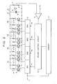
- FIG. 2 A capacitor 6, having a large capacitance, is . connected in parallel with a DC power source 5.
- DC power source 5 has a current capacity smaller than current necessary to simultaneously drive all thermal resistive elements.
- the elements are placed in, for example, four groups, Rl-14.
- Two series resistors 7, 8 are connected in parallel with capacitor 6 for detecting the terminal voltage of capacitor 6. The voltage detected by these resistors is compared in comparator 9 with a predetermined reference voltage Vr.
- a shift register 2 is divided into four serially connected groups, SR1-SR4 consisting of a plurality of memory units, each group corresponding to a respective element group.
- the bit number of recording signals for one line is 1728
- the bit number of each group is 432 (i.e., 1728/4).
- Each of the groups SRI ... SR4 has a control terminal (i.e., Pl ... P4) which controls the output signals from that group. Namely, when a "1" signal is supplied to certain control terminals, the groups of shift register 2 receiving this signal will output the signals stored within these groups to drive elements 3. On the other hand, when an "0" signals is supplied to certain output control terminals, the group receiving this signal will be prevented from activating the drive elements serially connected thereto.
- the control signals are supplied from a record control circuit 10.
- record control circuit 10 supplies a "1" control signal to all the output control terminals; consequently, all groups are activated to to permit the elements 4 to be driven by the appropriate recording signals.
- a signal is supplied from comparator 9 to record control circuit 10 to change the state of one or more of the control signals supplied to terminals P1-P4.
- Record control circuit 10 outputs "0" control signals to certain ones of the output control terminals Pl .. P4 according to the number of black recording signals stored in each section of memory 11, as will be explained later.
- the capacitance of capacitor 6 is selected so that degradation of density at several lines is prevented even assuming the total current flowing through all the resistive elements is temporarilly greater than the current capacity I 0 .
- the width of the resistive signal pulse flowing through elements 4 is 1 msec
- the duty cycle of the resistive signal pulses is 50 %
- the current capacity I 0 is 26A
- the simultaneous driving current Ia is 104A.
- the capacitance C of capacitor 6 is selected to be about 0.304 farads. If the duty cycle of the recording signal pulse is 75 %, the capacitance C becomes about 0.361 farads by the following calculation electrolytic capacitor of electric double layer type is the preferable type capacitor due to its compactness, practicality, and large capacitance values.
- FIG. 3 shows an example of the change of the terminal voltage of capacitor 6 versus time.
- V 0 is the controllable maximum voltage of DC power source 5 and initial voltage.
- Vl is the controllable minimum voltage of DC power source 5 and V2 is the minimum voltage necessary for recording.
- I S (see Fig. 2) is the current output of source 5 and It is the current flowing in the branch of the circuit. containing resistive elements 4.
- I l has a value I ll when all the. resistive elements in one group are activated and all the other groups are simultaneously deactivated.
- I l has a value I l1 when some but not all of the resistive elements in a group is activated and all the other groups are deactivated.
- I l has the value I ll , I l ⁇ I 0 ; when I l has the value I l1 , I l ⁇ I 0 .
- record control circuit 10 supplies output control signals having a "0" value to certain output control terminals and a "1" value to other terminals according to the number of black signals stored in each section of memory 11 for one line. That is, record control circuit 10 calculates the total current flowing within each respective group (e.g., I 1 ... I4) of resistive elements 4 from the pattern of recording signals stored in memory 11. For example, if memory 11 contains four black recording signals in the memory section corresponding to group one of resistive elements, then the total current I l in group one will equal 4 V 2 /R s where R s is the resistance of each resistive element.
- record control circuit 10 first calculates I3 + I 4 and compares it with I 0 . If I3 + I4 > I 0 , then a "1" signal is supplied only to output control terminal P4 during a predetermined time. During this predetermined time, the other output terminals are supplied with a "0" signal. Immediately after this predetermined time, record control circuit 10 then calculates 1 2 + I 3 and compares it with I 0 . If I 2 + I3 > I 0 , a "1" signal is then supplied only to output control terminal P3 during a second predetermined time. During this second predetermined time, the other output terminals are supplied with an "0" signal.
- record control circuit 10 calculates I 1 + I 2 and compares it with I 0 . If I 1 + I 2 > I 0 , a "1" signal is then sequentially supplied to control terminals P2 and Pl during a third and forth predetermined time respectively. During this third and forth predetermined time, the other output terminals are supplied with a "0" signal.
- each group of the four groups of thermal resistive elements are activated in sequence.
- a "1" signals is supplied into the two respective terminals at the same time.
- I l + I 2 ⁇ I 0 a "1" signal is simultaneously supplied to control terminals Pl and P2. That is, the two groups Rl and R2 of thermal resistive elements 4 are simultaneously driven.
- V V2
- memory 11 can be deleted in that case, when the terminal voltage falls below V2 and comparator 9 supplies a signal to record control circuit 10, record control circuit 10 will supply a "1" signal in sequence to output control terminals P4, P3, P2, and Pl. During each time period when a "1" signal is supplied to a signal terminal, the other terminals are supplied with an "0" signal.
- the resistive elements 4 are divided into several groups (e.g., four groups - Rl ... R4) and connected to switching elements (e.g., transistors Sl ... S4).
- switching element S4 by record control circuit 10 (i.e., "1" signal) while deactivating switching elements Sl - S3 (i.e., "0" signal) permits operation only of the resistor elements in group four by appropriate recording signals. Subsequently, S3 is activated while Sl - S2 and S4 are deactivated. Thereafter, S2 is activated while Sl and S3 - S4 are deactivated, and finally Sl is activated while S2 - S4 is deactivated.
- the decrease of terminal voltage V of capacitor 6 is directly detected by resistors 7 and 8. It is possible, however, to indirectly detect the voltage decrease.
- the decrease in voltage can indirectly be detected by using a counter 12 which counts the number of black recording signals.
- Counter 12 counts the number of black recording signals which occurred during the previous recording of a predetermined number of lines.
- record control circuit 10 supplies a "1" signal in sequence to output control terminals P4, P3, P2 and Pl in the manner discussed above regarding Figure 4.
Landscapes
- Engineering & Computer Science (AREA)
- Multimedia (AREA)
- Signal Processing (AREA)
- Physics & Mathematics (AREA)
- General Physics & Mathematics (AREA)
- Electronic Switches (AREA)
- Dot-Matrix Printers And Others (AREA)
- Facsimile Heads (AREA)
- Fax Reproducing Arrangements (AREA)
Applications Claiming Priority (2)
| Application Number | Priority Date | Filing Date | Title |
|---|---|---|---|
| JP55031279A JPS6027577B2 (ja) | 1980-03-12 | 1980-03-12 | 熱記録装置 |
| JP31279/80 | 1980-03-12 |
Publications (2)
| Publication Number | Publication Date |
|---|---|
| EP0035746A1 true EP0035746A1 (fr) | 1981-09-16 |
| EP0035746B1 EP0035746B1 (fr) | 1985-09-04 |
Family
ID=12326874
Family Applications (1)
| Application Number | Title | Priority Date | Filing Date |
|---|---|---|---|
| EP81101549A Expired EP0035746B1 (fr) | 1980-03-12 | 1981-03-04 | Dispositif d'enregistrement thermique |
Country Status (4)
| Country | Link |
|---|---|
| US (1) | US4360819A (fr) |
| EP (1) | EP0035746B1 (fr) |
| JP (1) | JPS6027577B2 (fr) |
| DE (1) | DE3172100D1 (fr) |
Cited By (5)
| Publication number | Priority date | Publication date | Assignee | Title |
|---|---|---|---|---|
| EP0079208A3 (en) * | 1981-11-06 | 1984-10-10 | Fuji Xerox Co., Ltd. | Picture data recording apparatus |
| EP0156360A3 (en) * | 1984-03-26 | 1986-12-30 | Tokyo Electric Co., Ltd. | Thermal dot type printing apparatus |
| WO1988005242A1 (fr) * | 1987-01-02 | 1988-07-14 | Eastman Kodak Company | Circuit generateur de formes d'onde modulees en largeur d'impulsion centrale et imprimante de type sans impact utilisant ce circuit |
| WO1989002825A1 (fr) * | 1987-10-02 | 1989-04-06 | Siemens Aktiengesellschaft | Procede d'impression thermique de supports |
| EP0390444A3 (fr) * | 1989-03-31 | 1992-01-08 | Toshiba Intelligent Technology Ltd. | Imprimante thermique pour terminal de données portable |
Families Citing this family (22)
| Publication number | Priority date | Publication date | Assignee | Title |
|---|---|---|---|---|
| JPS57128570A (en) | 1981-02-03 | 1982-08-10 | Canon Inc | Printer |
| JPS57156282A (en) * | 1981-03-24 | 1982-09-27 | Fuji Xerox Co Ltd | Driving method of thermo sensitive recording head |
| JPS585280A (ja) * | 1981-07-03 | 1983-01-12 | Canon Inc | 画像記録方法 |
| JPS5821117A (ja) * | 1981-07-30 | 1983-02-07 | Shimadzu Corp | パラレルヘツド記録計 |
| JPS5831777A (ja) * | 1981-08-19 | 1983-02-24 | Ishida Scales Mfg Co Ltd | サ−マルプリンタ−の不良素子回避方法 |
| JPS5871174A (ja) * | 1981-09-22 | 1983-04-27 | Fujitsu Ltd | 過負荷印字制御方式 |
| JPS58208069A (ja) * | 1982-05-29 | 1983-12-03 | Fujitsu Ltd | 過負荷印字制御方式 |
| JPS59227471A (ja) * | 1983-06-09 | 1984-12-20 | Matsushita Electric Ind Co Ltd | 感熱記録用ヘツド |
| JPH0764096B2 (ja) * | 1983-06-24 | 1995-07-12 | キヤノン株式会社 | 記録装置 |
| US4724033A (en) * | 1984-04-03 | 1988-02-09 | Monarch Marking Systems, Inc. | Hand-held labeler having improved web position sensing and print head control |
| JPS60245559A (ja) * | 1984-05-21 | 1985-12-05 | Fujitsu Ltd | 電圧検出レベル切替方法 |
| JPH0761117B2 (ja) * | 1984-08-31 | 1995-06-28 | 富士ゼロックス株式会社 | 感熱記録方法および装置 |
| JPH06102382B2 (ja) * | 1984-12-28 | 1994-12-14 | 富士通株式会社 | プリンタの分割印字装置 |
| US4638333A (en) * | 1985-10-25 | 1987-01-20 | Xerox Corporation | Thermal printing circuit |
| US4739344A (en) * | 1987-02-27 | 1988-04-19 | Astro-Med, Inc. | Chart recorded having multiple thermal print heads |
| JPS6450948U (fr) * | 1987-09-24 | 1989-03-29 | ||
| DE4214545C2 (de) * | 1992-04-29 | 1996-08-14 | Francotyp Postalia Gmbh | Anordnung für eine ETR-Druckkopfansteuerung |
| EP0568162A1 (fr) * | 1992-04-29 | 1993-11-03 | Francotyp-Postalia GmbH | Dispositif pour la commande d'une tête d'impression électrothermique |
| DE4221275C2 (de) * | 1992-06-26 | 1994-04-21 | Francotyp Postalia Gmbh | Ansteuerschaltung für eine elektrothermische Druckvorrichtung mit Widerstandsband |
| JP2002355970A (ja) * | 2001-05-31 | 2002-12-10 | Canon Inc | 記録装置 |
| JP4443407B2 (ja) * | 2002-07-25 | 2010-03-31 | アクララ バイオサイエンシーズ, インコーポレイテッド | レセプターオリゴマー形成の検出 |
| US8157340B2 (en) * | 2006-11-21 | 2012-04-17 | Intermec Ip Corp. | Apparatus and method for thermal printers that employ a battery or other portable power source |
Citations (6)
| Publication number | Priority date | Publication date | Assignee | Title |
|---|---|---|---|---|
| US3934695A (en) * | 1974-09-23 | 1976-01-27 | Hewlett-Packard Company | Method and apparatus for enhancing and maintaining character quality in thermal printers |
| US3951247A (en) * | 1973-12-28 | 1976-04-20 | Ing. C. Olivetti & C., S.P.A. | Electrothermal printing unit |
| US4032925A (en) * | 1976-05-10 | 1977-06-28 | Northern Telecom Limited | Drive circuit for thermal printing array |
| US4141018A (en) * | 1976-11-08 | 1979-02-20 | Tokyo Shibaura Electric Co., Ltd. | Thermal recording head and drive circuit |
| US4149171A (en) * | 1977-01-27 | 1979-04-10 | Hitachi, Ltd. | Thermal recording method |
| US4219824A (en) * | 1978-01-18 | 1980-08-26 | Hitachi, Ltd. | Thermal recording apparatus |
Family Cites Families (2)
| Publication number | Priority date | Publication date | Assignee | Title |
|---|---|---|---|---|
| JPS52141526A (en) * | 1975-10-27 | 1977-11-25 | Seiko Epson Corp | Voltage and temperature compensating control of thermal printer |
| JPS5353223A (en) * | 1976-10-25 | 1978-05-15 | Epson Corp | Circuit for compensating voltage of thermal printer |
-
1980
- 1980-03-12 JP JP55031279A patent/JPS6027577B2/ja not_active Expired
-
1981
- 1981-03-04 DE DE8181101549T patent/DE3172100D1/de not_active Expired
- 1981-03-04 EP EP81101549A patent/EP0035746B1/fr not_active Expired
- 1981-03-05 US US06/240,970 patent/US4360819A/en not_active Expired - Lifetime
Patent Citations (6)
| Publication number | Priority date | Publication date | Assignee | Title |
|---|---|---|---|---|
| US3951247A (en) * | 1973-12-28 | 1976-04-20 | Ing. C. Olivetti & C., S.P.A. | Electrothermal printing unit |
| US3934695A (en) * | 1974-09-23 | 1976-01-27 | Hewlett-Packard Company | Method and apparatus for enhancing and maintaining character quality in thermal printers |
| US4032925A (en) * | 1976-05-10 | 1977-06-28 | Northern Telecom Limited | Drive circuit for thermal printing array |
| US4141018A (en) * | 1976-11-08 | 1979-02-20 | Tokyo Shibaura Electric Co., Ltd. | Thermal recording head and drive circuit |
| US4149171A (en) * | 1977-01-27 | 1979-04-10 | Hitachi, Ltd. | Thermal recording method |
| US4219824A (en) * | 1978-01-18 | 1980-08-26 | Hitachi, Ltd. | Thermal recording apparatus |
Cited By (5)
| Publication number | Priority date | Publication date | Assignee | Title |
|---|---|---|---|---|
| EP0079208A3 (en) * | 1981-11-06 | 1984-10-10 | Fuji Xerox Co., Ltd. | Picture data recording apparatus |
| EP0156360A3 (en) * | 1984-03-26 | 1986-12-30 | Tokyo Electric Co., Ltd. | Thermal dot type printing apparatus |
| WO1988005242A1 (fr) * | 1987-01-02 | 1988-07-14 | Eastman Kodak Company | Circuit generateur de formes d'onde modulees en largeur d'impulsion centrale et imprimante de type sans impact utilisant ce circuit |
| WO1989002825A1 (fr) * | 1987-10-02 | 1989-04-06 | Siemens Aktiengesellschaft | Procede d'impression thermique de supports |
| EP0390444A3 (fr) * | 1989-03-31 | 1992-01-08 | Toshiba Intelligent Technology Ltd. | Imprimante thermique pour terminal de données portable |
Also Published As
| Publication number | Publication date |
|---|---|
| US4360819A (en) | 1982-11-23 |
| DE3172100D1 (en) | 1985-10-10 |
| EP0035746B1 (fr) | 1985-09-04 |
| JPS6027577B2 (ja) | 1985-06-29 |
| JPS56127469A (en) | 1981-10-06 |
Similar Documents
| Publication | Publication Date | Title |
|---|---|---|
| EP0035746A1 (fr) | Dispositif d'enregistrement thermique | |
| EP0036965B1 (fr) | Dispositif d'enregistrement thermique | |
| US4475114A (en) | Thermal head recording device | |
| EP0068702B1 (fr) | Imprimante thermique | |
| US5457488A (en) | Method and apparatus for controlling array of light-emitting elements | |
| EP0716927A2 (fr) | Dispositif à tête thermique | |
| US4560993A (en) | Thermal printing method and thermal printer | |
| EP0061314B1 (fr) | Dispositif d'enregistrement sensible à la chaleur | |
| EP0186508A2 (fr) | Dispositif de distribution pour impression par points | |
| US4656489A (en) | Thermal printer/plotter | |
| US4590485A (en) | Thermal recorder | |
| JPH0257507B2 (fr) | ||
| EP0079208A2 (fr) | Appareil d'enregistrement de données d'image | |
| US4642657A (en) | Recorder | |
| US4568948A (en) | Driving system for thermal recording head | |
| EP0185910A1 (fr) | Dispositif de commande pour imprimante thermique | |
| US5528275A (en) | Gradational printing method | |
| EP0068126B1 (fr) | Système d'enregistrement électrostatique et circuit d'excitation de stylet pour celui-ci | |
| US4459462A (en) | Drive system for energizing elements of a fixed bar printer | |
| JPS58173682A (ja) | サ−マルヘツド駆動装置 | |
| JP2611197B2 (ja) | 感熱ヘツドの駆動制御回路 | |
| EP0680827B1 (fr) | Tête d'impression électrostatique | |
| WO1987007219A1 (fr) | Circuit de commande d'energie d'une imprimante | |
| JPS6076360A (ja) | 感熱記録装置 | |
| JPH02249662A (ja) | 通電記録装置 |
Legal Events
| Date | Code | Title | Description |
|---|---|---|---|
| PUAI | Public reference made under article 153(3) epc to a published international application that has entered the european phase |
Free format text: ORIGINAL CODE: 0009012 |
|
| AK | Designated contracting states |
Designated state(s): DE FR GB NL SE |
|
| 17P | Request for examination filed |
Effective date: 19810304 |
|
| RAP1 | Party data changed (applicant data changed or rights of an application transferred) |
Owner name: KABUSHIKI KAISHA TOSHIBA |
|
| GRAA | (expected) grant |
Free format text: ORIGINAL CODE: 0009210 |
|
| AK | Designated contracting states |
Designated state(s): DE FR GB NL SE |
|
| PG25 | Lapsed in a contracting state [announced via postgrant information from national office to epo] |
Ref country code: NL Effective date: 19850904 |
|
| PG25 | Lapsed in a contracting state [announced via postgrant information from national office to epo] |
Ref country code: SE Effective date: 19850930 |
|
| REF | Corresponds to: |
Ref document number: 3172100 Country of ref document: DE Date of ref document: 19851010 |
|
| ET | Fr: translation filed | ||
| NLV1 | Nl: lapsed or annulled due to failure to fulfill the requirements of art. 29p and 29m of the patents act | ||
| PLBE | No opposition filed within time limit |
Free format text: ORIGINAL CODE: 0009261 |
|
| STAA | Information on the status of an ep patent application or granted ep patent |
Free format text: STATUS: NO OPPOSITION FILED WITHIN TIME LIMIT |
|
| 26N | No opposition filed | ||
| REG | Reference to a national code |
Ref country code: GB Ref legal event code: 746 Effective date: 19981126 |
|
| PGFP | Annual fee paid to national office [announced via postgrant information from national office to epo] |
Ref country code: DE Payment date: 19991231 Year of fee payment: 20 |
|
| PGFP | Annual fee paid to national office [announced via postgrant information from national office to epo] |
Ref country code: GB Payment date: 20000301 Year of fee payment: 20 |
|
| PGFP | Annual fee paid to national office [announced via postgrant information from national office to epo] |
Ref country code: FR Payment date: 20000310 Year of fee payment: 20 |
|
| REG | Reference to a national code |
Ref country code: FR Ref legal event code: D6 |
|
| PG25 | Lapsed in a contracting state [announced via postgrant information from national office to epo] |
Ref country code: GB Free format text: LAPSE BECAUSE OF EXPIRATION OF PROTECTION Effective date: 20010303 |
|
| REG | Reference to a national code |
Ref country code: GB Ref legal event code: PE20 Effective date: 20010303 |