EP0037239A2 - Dispositif de mémoire de type dynamique à semi-conducteurs comprenant un circuit d'écriture-lecture de données - Google Patents
Dispositif de mémoire de type dynamique à semi-conducteurs comprenant un circuit d'écriture-lecture de données Download PDFInfo
- Publication number
- EP0037239A2 EP0037239A2 EP81301269A EP81301269A EP0037239A2 EP 0037239 A2 EP0037239 A2 EP 0037239A2 EP 81301269 A EP81301269 A EP 81301269A EP 81301269 A EP81301269 A EP 81301269A EP 0037239 A2 EP0037239 A2 EP 0037239A2
- Authority
- EP
- European Patent Office
- Prior art keywords
- write
- data
- signal
- circuit
- buffer
- Prior art date
- Legal status (The legal status is an assumption and is not a legal conclusion. Google has not performed a legal analysis and makes no representation as to the accuracy of the status listed.)
- Granted
Links
Images






Classifications
-
- G—PHYSICS
- G11—INFORMATION STORAGE
- G11C—STATIC STORES
- G11C5/00—Details of stores covered by group G11C11/00
- G11C5/06—Arrangements for interconnecting storage elements electrically, e.g. by wiring
- G11C5/066—Means for reducing external access-lines for a semiconductor memory clip, e.g. by multiplexing at least address and data signals
-
- G—PHYSICS
- G11—INFORMATION STORAGE
- G11C—STATIC STORES
- G11C11/00—Digital stores characterised by the use of particular electric or magnetic storage elements; Storage elements therefor
- G11C11/21—Digital stores characterised by the use of particular electric or magnetic storage elements; Storage elements therefor using electric elements
- G11C11/34—Digital stores characterised by the use of particular electric or magnetic storage elements; Storage elements therefor using electric elements using semiconductor devices
- G11C11/40—Digital stores characterised by the use of particular electric or magnetic storage elements; Storage elements therefor using electric elements using semiconductor devices using transistors
- G11C11/401—Digital stores characterised by the use of particular electric or magnetic storage elements; Storage elements therefor using electric elements using semiconductor devices using transistors forming cells needing refreshing or charge regeneration, i.e. dynamic cells
- G11C11/4063—Auxiliary circuits, e.g. for addressing, decoding, driving, writing, sensing or timing
- G11C11/407—Auxiliary circuits, e.g. for addressing, decoding, driving, writing, sensing or timing for memory cells of the field-effect type
- G11C11/409—Read-write [R-W] circuits
- G11C11/4093—Input/output [I/O] data interface arrangements, e.g. data buffers
Definitions
- This invention relates to a semiconductor memory device, and more particularly to a data read/write portion of a dynamic memory device.
- a semiconductor memory device consists basically of a row circuit for driving word lines, a column circuit for driving bit lines and for executing writing or reading operations, and a number of memory cells connected between the word lines and the bit lines, for storing information therein.
- the present invention mainly relates to the column circuit, which is, in other words, a data read/write portion of the semiconductor memory device.
- An embodiment of the present invention can provide a dynamic semiconductor memory device, in which power consumption is reduced in comparison with a conventional device, without increasing the number of pins on the device.
- An embodiment of the present invention can provide a semiconductor memory device, in which a data write-in buffer included in a column circuit of the device is of a dynamic type.
- a semiconductor memory device of a dynamic type including a read/write circuit in a column circuit for reading data from or writing data into a memory cell in response to column driving signals.
- the read/write circuit comprises a common input/output terminal (I/O) for inputting write data into or for outputting read data from the memory cell; a data output buffer (DOB) for outputting read data to the I/0 terminal from the memory cell; a three-state circuit (Qa, Qb) connected between the common input/output terminal and the data output buffer for setting the common input/output terminal to a high impedance or a state according to read data; a data write-in buffer (DWB) having a latching function connected between the common input/output terminal and the memory cell; a first means for turning off the three-state circuit so as to set the common input/output terminal to a high impedance, in response to one state of the column circuit driving signals; and, a second means for latching write data applied to the common input/out
- the data write-in buffer is a dynamic circuit comprising a bistable circuit for latching the write data and a write-in circuit for writing the latched-write data into said memory cell.
- the column circuit driving signals comprises a write enable signal for setting the read/write circuit to a write enable state when the write enable signal is turned on;
- the first means comprises a latching circuit for providing a latched driving signal, in response to a turning on of said write enable signal, said latched driving signal being used to keep the three-state circuit in the off state even after the write enable signal is turned off.
- second means comprises a gate circuit having a first input for receiving said latched driving signal and a second input for receiving the write enable signal, the gate circuit being adapted to provide a data write-in buffer-driving signal for setting the data write-in buffer to an enable state so as to latch the write data, in response to the turning off of the write enable signal.
- the column circuit driving signals comprises a write enable signal and a column-address strobe signal, the column--address strobe signal being used to set the data output buffer to a write enable state when the column-address strobe signal is turned off, the first means being adapted to keep the common input/output terminal to a high impedance when the column-address strobe signal is turned off; and, the second means comprises; a latching circuit for providing a latched signal to keep the column-address strobe signal on even after said column-address strobe signal is turned off; and, a write-enable buffer for providing a driving signal which is inputted to the data write-in buffer, the driving signal being provided when both the write-enable signal and the latched signal are applied to the write-enable buffer, the data write-in buffer being adapted to latch the write data when the data write-in buffer receives the driving signal.
- the capacity of the semiconductor memory device has been more and more increased.
- a memory device of 1-bit 4k words, 1-bit 16k words, 1-bit 32 k words, or 1-bit 64k words is known.
- the number of locations available that is, the number of words is nk, each word consisting of m bits.
- the 1-bit 64k-word memory device will be explained as an example.
- Fig. 1A is a schematic diagram for illustrating the structure of the 1-bit 64k-word memory device.
- the memory device of 1-bit 64k words has 64k memory cells MC. Each memory cell corresponds to one of 65,536 words. Therefore, each word consists of one bit.
- one of 256 word lines are specified by a row circuit, and then one of 256 bit lines are specified by a column circuit. For specifying one of the 256 bit lines, the column circuit must have eight address pins.
- Fig. 1B is a schematic plan view of the 1-bit 64k-word memory device, for illustrating input/output pins on the column decoder.
- the total number of the input/output pins is fifteen.
- F ig. 2A is a schematic diagram for illustrating the structure of the 4-bits 16k-word memory device.
- the 4-bit 16k-word memory device has also 64k memory cells MC.
- the number of locations available, that is, the number of words is 16k.
- Each word consists of four bits.
- four-bit data can be dealt with.
- one of 128 word lines are specified by a row circuit, and then one of 128 bit lines are specified by a column circuit.
- the memory device must have seven address pins.
- 4-bit data is inputted into or outputted from this 4-bit 16k-word memory device, four input pins and four output pins for data input/output are necessary.
- F ig. 2 B is a schematic plan view of the 4-bit 16k-word memory device, for illustrating input/output pins on the column circuit. On this device, there are also provided input pins Vcc, Vss, RAS, CAS and WE.
- the difference between Fig. 1B and Fig. 2B is that in Fig. 2B, seven address pins A 0 , A 1 , ... , A 6 , four input pins D in0 , D in1 , ... , and D in3 for data input, and four output pins D out0 , D out1 , ... and D o ut3 are provided.
- the total number of the input/output pins is twenty, which is greater than the total number of the input/output pins in Fig. 1B.
- each of data-input pins is also used as one of data-output pins.
- Figure 3 is a schematic plan view of a 4-bit 16k-word nemory device, in which pins are used in common as data-input pins and data-output pins. As can be seen from Figure 3, the total number of pins is sixteen, which is smaller than that of Figure 2B.
- Figure 4A is a block diagram for illustrating a part of a conventional column circuit of a dynamic memory device, in which a pin is used in common as a data-input pin and a data-output pin.
- the conventional column circuit 1 includes a column enable buffer CEB connected to the CAS pin for providing a column enable signal CE and its inverted signal CE, a write enable buffer WEB connected to the WE pin for providing a write enable siganl WE, a data output buffer DOB connected through a three-state circuit including transistors Q a and Q b to the common input/ output pin I/O ) and a static data write-in buffer SDWB connected to the pin I/O.
- the row enable buffer REB In a reading operation, after a row address strobe signal RAS is supplied to a row enable buffer REB, for providing a row enable signal RE and its inverse RE , so that one of the word lines is selected, the row enable buffer REB provides a signal to the column enable buffer CEB to set it to its enable state. Then, when the signal CAS turns to a low potential level (hereinafter referred to as the L level), the CEB generates CE and CE for input to the DOB and to the SDWB to set them in their enable states.
- the WEB since the WEB does not provide the signal WE to the DOB, at least one of the two transistors Q a and Q b is in an ON state. Therefore, data read from a memory cell (not shown) is transferred through the DOB and one of the transistors Q and Q b to the pin I/O.
- a writing operation is performed as follows.
- the write enable buffer WEB When the signal WE is turned to the L level, the write enable buffer WEB generates a write enable signal WE, which is then inputted into the data output buffer D O B to turn off the transistors Q a and Q b so that they present a high impedance to the I/O pin. In this state, it is possible for the I/O pin to receive write data.
- the write enable signal WE is inputted into the static data write-in buffer SDWB to set it in its enable state.
- the buffer SDWB receives the write data through the I/O pin so that the buffer SDWB sets the data bus DB connected to the cell specified by a word line and a bit line to a high potential level H or a low potential level L, according to the write data.
- a signal on the data bus DB also connected to the buffer SDWB is the inversion of the signal on the data bus DB.
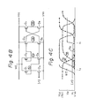
- Fig. 4B is a circuit diagram of the static data write-in buffer SDWB included in the circuit of Fig. 4A.
- transistors Q 1 and Q are depletion--type MOS transistors having negative threshold voltages; and other transistors Q 3 through Q 8 are enhancement-type MOS transistors having positive threshold voltages.
- the transistors Q 1 and Q 3 , as well as the transistors Q 2 and Q 4 are connected in series between the write enable input WE and the ground voltage Vss.
- the transistors Q 5 and Q 6 , as well as the transistors Q 7 and Q 8 are connected in series between the power supply voltage Vcc and the ground voltage Vss. Write data is applied to the I/O pin connected to the gate of the transistor Q 3 .
- the data bus DB is connected to a point between the source of the transistor Q 5 and the drain of the transistor Q 6 .
- the inverted data bus DB is connected to a point between the source of the transistor Q 7 and the drain of the transistor Q 8 .
- the gate of the transistor Q 1 is connected to its source, or a point N 1 , which is connected to the gates of the transistor Q 4 , Q 6 and Q .
- the gate of the transistor Q 2 is connected to its source, or a point N 2 , which is connected to the gates of the transistors Q 5 and Q 8 .
- Fig. 4C is a time chart for explaining the operation of the circuit of Fig. 4B. Referring to Figs. 4B and 4C, it is assumed that, at the first stage, the potential at the I/O pin is a lower threshold voltage V ; and the potential of the data bus DB is the high level. At a time t 0 , when the potential of the write enable signal W E is raised to the Vcc level, the potential at the point N 1 rises to the Vcc level so that the transistors Q 4 , Q 6 and Q7are turned on. In this state, current flows through the transistors Q 2 and Q 4 , and therefore, the potential at the point N 2 is kept at a low level so that the transistors Q5 and Q 8 are turned off.
- the transistor Q Since the transistor Q is turned on, charges on the data bus DB discharge through the transistor Q 6 to the ground voltage Vss. On the other hand, since the transistor Q 8 is in the off state, the inverted data bus DB is charged up from the power supply voltage Vcc through the transistor Q 7 . Then, at a time t 1 , when the potential at the I/O pin is raised to a higher threshold voltage V H , the transistor Q 3 is turned on so that the potential at the point N 1 falls to a low level; and current flows through the transistors Q 1 and Q 3 to the ground. Since the gate of the transistor Q 4 is lowered, the transistor Q 4 is turned off. Therefore, the point N 2 is charged up so that the potential at the point N 2 is raised to the high level. Thus, the potential levels of the data buses DB and DB are inverted.
- circuit of Fig. 4B is of a static type, data can be freely inputted without any clock signal. Therefore, regardless of the input timing, the last-in data is written into the connected memory cell.
- the data write-in buffer can be made as a dynamic type.
- clock signals for latching data are necessary.
- these clocks must be slightly delayed after the clocks for setting the three state circuit to be high impedance are applied to the data output buffer DOB. If the former clocks are applied at the same time when the latter clocks are applied, error data may be written into the memory cell.
- a special clock signal is employed, the possibility of writing error data is eliminated.
- the circuit will become complicated and the number of pins on the memory device will be increased.
- a data write-in buffer of a dynamic type is employed, which is operated without using a special clock signal.
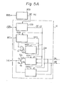
- Fig. 5A is a block diagram for illustrating a part of a column circuit of a dynamic memory device, according to an embodiment of the present invention.
- the main differences between the circuit of Fig. 5A and the conventional circuit of Fig. 4A reside in that, in place of the static data write-in buffer SDWB.in Fig. 4A, a dynamic data write-in buffer DWB having a function to latch input data is used in the circuit of Fig. 5A.
- an output disable buffer O D B having a latching function and an AND gate G 1 which were not provided in the circuit of Fig. 4A, are provided in the circuit of Fig. 5A.
- the output disable buffer ODB receives the inverted write enable signal WE and the column enable signals CE and CE for outputting a signal OPD which is inputted into the first input of the AND gate G 1 and into the data output buffer DOB.
- the AND gate G I also receives at its second input the inverted write enable signal WE.
- the output of the AND gate G 1 is connected to the write enable buffer WEB.
- the other connections are the same as those in the conventional circuit of Fig. 4A, and therefore are not described here.
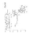
- Fig. 5B is a time chart for explaining the operation of the column circuit of Fig. 5A. Referring to Figs. 5A and 5B, reading operation will first be explained. After a row address strobe signal RAS is supplied to the row enable buffer REB so that one of the word lines is selected, the row enable buffer REB provides a signal to the column enable buffer CEB to set it in its enable state. Then, at a time t 01 , when the signal CAS turns to the L level, the CEB generates the signals CE and CE which are then input in parallel to ODB, WEB, DOB and DWB to set them in their enable states.
- RAS row address strobe signal
- the row enable buffer REB provides a signal to the column enable buffer CEB to set it in its enable state.
- the CEB generates the signals CE and CE which are then input in parallel to ODB, WEB, DOB and DWB to set them in their enable states.
- the DOB receives the signals CE and CE, the DOB sets at least one of the points Na or Nb to the high level.
- the points Na and Nb are connected to the gates of the transistors Qa and Qb, respectively. Therefore, at least one of the transistors Qa or Qb is turned on so that the state of the I/O pin is changed from high impedence HZ to the state according to the read data.
- data read from the memory cell (not shown) is transferred through the DOB and one of the transistors Qa and Qb to the I/O pin.
- the reading term is the time interval between the time t 01 and the time t 11 .
- the ODB begins to operate so that its output signal OPD is turned to the H level.
- the H level signal O PD is supplied to the first input of the AND gate G 1 and to the DOB.
- the DOB receives the H level signal OPD
- the D OB turns the potential level of the points Na and Nb to the low level.
- the transistors Qa and Qb are turned off so that the state of the I/O pin becomes high impedance HZ.
- write data WD is inputted at the I/O pin.
- the signal WE is turned to the H level (turned offf) Since the ODB has the latching function, the output signal OPD is kept at the H level after the signal WE is turned to the H level. Accordingly, the output N 33 of the AND gate G 1 becomes the H level so that the WEB begins to operate to turn its output signal DW to the H level.
- the DWB receives the H level signal DW, the DWB receives write data from the I/O pin and latches it. Then the data is outputted through the data buses DB and DB to the memory cell to be written therein.
- the signal RAS and the signal CAS are turned to the H level so that the signal CE is turned to the H level.
- the H level signal CE resets all of the circuits ODB, WEB, DOB and DWB.
- the I/O pin is kept at the high impedance HZ.
- writing operation is performed.
- the time t31 it is the reset interval RST.
- the I/O pin is turned to the high impedance HZ by using the fall of the signal WE as a clock signal.
- the writing operation can be started by using the rise of the signal WE as a clock signal.
- the data write-in buffer DWB can be made as a dynamic circuit.
- Fig. 5C is a circuit diagram of the output disable buffer ODB.
- the ODB consists of depletion-type MOS transistors Q 11 and Q 15 , enhancement-type MOS transistors Q 12 , Q 13 , Q14 and Q 16 , and an amplifier AMP .
- the transistors Q 11 and Q 12 , as well as the transistors Q 15 and Q 16 are connected in series between the column enable input CE and the ground voltage V ss .
- the transistors Q 13 and Q 14 are connected in series between the power supply voltage V cc and the ground voltage V .
- the amplifier AMP is connected between the power supply voltage Vcc and the ground voltage V ss .
- the gate and the source of cc ss the transistor Q 11 , the drain of the transistor Q 12 and the gate of the transistor Q 14 are connected to a point N 11 .
- the scurce of the transistor Q13 , the drain of the transistor Q 14 and the gate of the transistor Q 16 are connected to a point N 12 .
- the gate and the source of the transistor Q 15 , and the drain of the transistor Q 16 are connected to a point N 13 which is connected to an input of the amplifier AMP.
- the amplifier provides the output signal OPD.
- FIG. 5D An example of the circuit diagram of the amplifier AMP is illustrated in Fig. 5D.
- the amplifier AMP consists of transistors Q 17 through Q 28 . Since this amplifier AMP is a conventional amplifier, further explanation of this amplifier AMP is not given here.
- Fig. 5E is a circuit diagram of the AND gate G 1 .
- the AND gate G 1 consists of enhancement-type MOS transistors Q 31 , Q 32 , Q 33 and Q 35 , and a depletion-type MOS transistor Q 34 .
- the transistors Q 31 , Q 32 and Q 33 are connected in series between the power supply voltage V cc and the ground voltage V ss .
- the transistors Q 34 and Q 35 are connected in series between the output OPD of the ODB and the ground voltage V ss .
- the source of the transistor Q 31 , the drain of the transistor Q 32 and the gate of the transistor Q 35 are connected to a point N 31 .
- the source of the transistor Q 32 and the drain of the transistor Q 33 are connected to a point N 32 .
- the gate and the source of the transistor Q34 , and the drain of the transistor Q 35 are connected to a point N 33 which is connected to an input of the WEB (Fig. 5A).
- the gate of the transistor Q 31 receives the inverted column enable signal CE.
- the gate of the transistor Q 32 receives the inverted write enable signal WE.
- the gate of the transistor Q 33 and the drain of the transistor Q34 receive the output signal OPD from the output disable buffer ODB (Fig. 5A).
- Fig. 5F is a circuit diagram of a part of the data write-in buffer DWB.
- this circuit is a flip-flop, that is, a latching circuit, including transistors Q 51 , Q 52 , ... , and Q 63 .
- the drains of the transistors Q 51 , Q 52 , Q 57 and Q 58 are connected to the power supply voltage V cc .
- the source of the transistor Q 51 is connected through a point N 51 to the drain of the transistor Q 55 .
- the source of the transistor Q 52 is connected through a point N 52 to the drain of the transistor Q 56 .
- the gates of the transistor Q 53 and Q 57 are connected to the point N 51 .
- the gates of the transistors Q 54 and Q 58 are connected to the point N 52 .
- the source of the transistor Q 57 is connected through a point N 53 to the drains of the transistors Q 59 and Q 62 connected in parallel.
- the source of the transistor Q 58 is connected through a point N 54 to the drains of the transistors Q 60 and Q 63 connected in parallel.
- the gates of the transistors Q 56 and Q 60 , and the source of the transistor Q 55 are connected to the point N 53 .
- the gates of the transistors Q 55 and Q 59 , and the source of the transistor Q 56 are connected to the point N 54 .
- the source of the transistor Q 61 is connected to the ground voltage Vs s .
- the gates of the transistors Q 51 and Q 52 are adapted to receive the inverted column enable signal CE.
- the drain of the transistor Q 53 is connected to its source.
- the drain of the transistor Q 54 is connected to its source.
- the transistors Q 53 and Q 54 are adapted to receive the output signal DW from the write enable buffer WEB (Fig. 5A).
- the gate of the transistor Q62 is adapted to receive write data from the I/O pin.
- the gate of the transistor Q 63 receives a reference voltage REF which is typically 1.6V.
- Fig. 5G is a circuit diagram of the other part of the data write-in buffer DWB. Referring to Fig. 5G, this circuit has a function to write the data latched in the circuit of Fig. 5F into the memory cell (not shown), including transistors Q 64 , Q 65 , ..., and Q 70 .
- the drains of the transistors Q 64 and Q 67 are connected to the power supply voltage V cc .
- the source of the transistors Q 64 is connected through a point N 56 to the drain of the transistor Q 65 .
- the source of the transistor Q 67 is connected through a point N 57 to the drain of the transistor Q 68 .
- the sources of the transistors Q 65 and Q 68 are connected through a point N 58 to the drain of the transistor Q 70 .
- the source of the transistor Q 70 is connected to the ground voltage V ss .
- the source of the transistor Q 66 is connected to the point N 56 .
- the source of the transistor Q 69 is connected to the point N 57 .
- the gate of the transistor Q 64 is connected to the point N 53 ( F ig. 5F) and to the gate of the transistor Q68.
- the gate of the transistor Q 65 is connected to the point N 54 (Fig. 5F) and to the gate of the transistor Q 67 .
- the gates of the transistors Q 66 , Q 69 and Q 70 are adapted to receive the output signal DW from the write enable buffer WEB (Fig. 5A).
- the drain of the transistor Q 66 is connected to the inverted data bus DB.
- the drain of the transistor Q69 is connected to the data bus DB.
- Fig. 5H illustrates time.charts for explaining the operations of the circuits of Figs. 5C through 5F.
- the operation of the output disable buffer ODB will now be explained.
- the column enable signal CE is H level and therefore the inverted column enable signal CE is L level so that the output disable buffer is in its enable state.
- the inverted write enable signal WE applied to the gate of the transistor Q12 is H level. Therefore, at this time t 02 , the potential at the point N 11 is the L level. Since the transistor Q14 is in an off state because its gate connected to the point N 11 is the L level, the potential at the point N 12 is kept at the H level which has been charged up before the signal CE is turned to the L level.
- the transistor Q16 since the transistor Q16 is in an on state because of its gate connected to the point N 12 is the H level, the point N 13 is the L level. Then, at a time t 12 , the inverted write enable signal WE is turned to the L level. The transistor Q12 is then turned off so that the point N 11 connected to its drain is charged up to be the H level. Because of the H level of the point N 11 , the transistor Q14 is turned on so that the point N 12 is discharged to be the L level. Then, the transistor Q16 is turned off so that the point N 13 is charged up to the H level.
- the H level signal at the point N 13 is amplified by the amplifier AMP which provides the H level output OPD at a time t 22 when the H level output OPD is given to the DOB (Fig. 5A), the I/O pin becomes high impedance HZ as hereinbefore described. Then, after write data is applied to the I/O pin, at a time t32 , the inverted write enable signal WE is turned again to the H level. Thus, the transistor Q12 is turned on so that the point N 11 is discharged to be the L level. The L level of the point N 11 turns off the transistor Q 14 . However, since the inverted column enable signal CE is the L level, the point N 12 is not charged up. Therefore, even after the time t32 , the point N 13 and thus the output signal OPD is kept at the H level.
- the constitution of the write enable buffer WEB (Fig. 5A) is substantially the same as that of the amplifier 10 illustrated in Fig. 5D. Since the amplifier 10 is a well known one, the operations of the amplifier 10 and the write enable buffer WEB are not explained here.
- Figs. 5F, 5G and the lower portion of Fig. 5H the operation of the data write-in buffer DWB will be explained.
- the DWB begins to operate so that the write data from the I/O pin is latched in it and then the latched data is written through the data buses DB and DB to the memory cell.
- the point N 55 is discharged to be the L level; and, the transistors Q 53 and Q 54 used as capacitors boost up the potential of the points N 51 and N 52 connected to their gates.
- the write data from the I/O pin is the H level
- the point N 53 is discharged to the L level and the point N 54 is kept at the H level, therefore, the point N 51 is discharged through the transistor Q 55 .
- the point N 52 is not discharged and further boosted up to be a higher level than the V cc level, because the transistor Q 56 is turned off. Therefore, the point N 54 is charged up to the V cc level.
- the L level of the point N 53 and the H level of the point N 54 are latched in their states. In this state, the transistors Q 57 and Q 60 are cut off, and the transistors Q 58 and Q 59 are on. Therefore, the circuit illustrated in Fig. 5F does not consume the DC power. Also, the circuit illustrated in Fig. 5G does not consume the DC power.
- the L level signal at the point N 53 is applied to the gates of the transistors Q 64 and Q 68 .
- the H level signal at the point N 54 is applied to the gates of the transistors Q b5 and Q 67 .
- the H level output DW is also applied to the gates of the transistors Q 66 , Q 69 and Q 70 . Therefore, the point N 56 is discharged and the point N S7 is charged up. Accordingly, at a time t52 , the potential of the data bus D B rises to be the H level, while the potential of the data bus DB falls to the L level.
- F ig. 6A is a block diagram for illustrating a part of a column circuit of a dynamic memory device, according to another embodiment of the present invention.
- the column circuit according to this second embodiment includes also the column enable buffer CEB, the write enable buffer WEB, the data output buffer DOB, the data write-in buffer DWB, which are all included in the column circuit of the first embodiment, and a latching circuit LT.
- the inverted row enable signal RE is inputted not only to the CEB but also to the WEB, the DOB, DWB, and the LT so that RE resets these circuits.
- the column enable signal CE from the CEB is inputted to the LT and the DOB.
- the LT outputs a latched column enable signal LCE which is supplied to the WEB. Also, the signal LCE is supplied to the other circuits in this column circuit instead of the signal CE in Fig. 5A.
- the output signal DW from the WEB is inputted to the DWB.
- the other constitution is the same as the column decoder of Fig. 5A.
- Fig. 6B is a time chart for explaining the operation of the column circuit of Fig. 6A.
- the inverted row address strobe signal RAS is turned to the L level so that the row enable buffer REB is set to its enable state.
- the inverted row enable signal RE is accordingly turned to the'L level, and the row enable signal RE to the H level.
- the column address strobe signal CAS is turned to the L level.
- the column enable signal CE and the latched column enable signal LCE are turned to the H level.
- the WEB is then set to its enable state by the H level of the signal LCE from the latching circuit LT.
- the DOB is set to its enable state by the H level of the signal CE from the CEB.
- I/O pin outputs the read data from the memory cell through the data buses DB and DB, the DOB, and the three-state circuit to the I/O pin.
- the signal CAS is turned to the H levels
- the signal CE is turned to the L level.
- the DOB receives the L level signal CE, it turns off the transistors Qa and Qb resulting in high impedance at the I/O pin.
- the latched column enable signal LCE is kept at the H level even when the signal CE has been turned to the L level. Therefore, the WEB is in its enable state after the time t 23 . Then, at a time t 33 , when the inverted write enable signal WE is turned to the H level, the WEB outputs the H level signal DW which is inputted to the DWB. Thus, write data is latched and then written into the memory cell through the data buses DB and DB.
- a data write-in buffer in a column decoder is of a dynamic type, power consumption in a semiconductor memory device can be reduced in comparison with a conventional semiconductor memory device.
- no additional clock signal is required to drive the data write-in buffer, the number of pins is not increased.
- the present invention may be adapted to a semiconductor memory device having any memory capacity, and is not restricted to the forgoing embodiments. Various changes and modifications are possible without departing from the basic idea and scope of the invention.
- the inverted write enable signal WE is a write enable signal which is inverted as compared with a write enable signal WE.
- an embodiment of the present invention provides a semiconductor memory device of a dynamic type, including a read/write circuit in a column circuit in which one pin is used in common as a data input pin and a data output pin.
- the read/write circuit comprises a data output buffer (DOB) connected through a three-state circuit (Q a , Q b ) to the common data input/ output terminal (I/O), and a data write-in buffer of a dynamic type having a latching function and being connected between the common data input/output terminal and data buses ) for providing latched data to the data buses.
- DOB data output buffer
- Q a , Q b common data input/ output terminal
- a data write-in buffer of a dynamic type having a latching function and being connected between the common data input/output terminal and data buses ) for providing latched data to the data buses.
Landscapes
- Engineering & Computer Science (AREA)
- Microelectronics & Electronic Packaging (AREA)
- Computer Hardware Design (AREA)
- Dram (AREA)
- Static Random-Access Memory (AREA)
Applications Claiming Priority (2)
| Application Number | Priority Date | Filing Date | Title |
|---|---|---|---|
| JP39260/80 | 1980-03-27 | ||
| JP55039260A JPS5951073B2 (ja) | 1980-03-27 | 1980-03-27 | 半導体記憶装置 |
Publications (3)
| Publication Number | Publication Date |
|---|---|
| EP0037239A2 true EP0037239A2 (fr) | 1981-10-07 |
| EP0037239A3 EP0037239A3 (en) | 1983-06-29 |
| EP0037239B1 EP0037239B1 (fr) | 1986-10-15 |
Family
ID=12548164
Family Applications (1)
| Application Number | Title | Priority Date | Filing Date |
|---|---|---|---|
| EP81301269A Expired EP0037239B1 (fr) | 1980-03-27 | 1981-03-25 | Dispositif de mémoire de type dynamique à semi-conducteurs comprenant un circuit d'écriture-lecture de données |
Country Status (5)
| Country | Link |
|---|---|
| US (1) | US4397001A (fr) |
| EP (1) | EP0037239B1 (fr) |
| JP (1) | JPS5951073B2 (fr) |
| DE (1) | DE3175484D1 (fr) |
| IE (1) | IE52366B1 (fr) |
Cited By (4)
| Publication number | Priority date | Publication date | Assignee | Title |
|---|---|---|---|---|
| EP0083229A3 (en) * | 1981-12-26 | 1985-12-04 | Fujitsu Limited | Semiconductor memory device |
| EP0092245A3 (en) * | 1982-04-20 | 1986-11-20 | Mostek Corporation | Functional command for semiconductor memory |
| EP0451000A1 (fr) * | 1990-03-09 | 1991-10-09 | Fujitsu Limited | Dispositif de mémoire à semi-conducteurs avec fonction de contrôle perfectionnée pour le bus pour les données |
| EP0644550A3 (fr) * | 1993-09-17 | 1995-11-15 | Oki Electric Ind Co Ltd | Circuit de commande pour DRAM. |
Families Citing this family (12)
| Publication number | Priority date | Publication date | Assignee | Title |
|---|---|---|---|---|
| JPS6052513B2 (ja) * | 1981-12-02 | 1985-11-19 | 富士通株式会社 | 半導体記憶装置 |
| JPS58203694A (ja) * | 1982-05-21 | 1983-11-28 | Nec Corp | メモリ回路 |
| DE3243496A1 (de) * | 1982-11-24 | 1984-05-24 | Siemens AG, 1000 Berlin und 8000 München | Integrierte halbleiterschaltung mit einem dynamischen schreib-lese-speicher |
| JPS59110090A (ja) * | 1982-12-14 | 1984-06-25 | Nec Corp | メモリ回路 |
| US4628480A (en) * | 1983-10-07 | 1986-12-09 | United Technologies Automotive, Inc. | Arrangement for optimized utilization of I/O pins |
| JPS60136086A (ja) * | 1983-12-23 | 1985-07-19 | Hitachi Ltd | 半導体記憶装置 |
| JPH063572B2 (ja) * | 1984-09-06 | 1994-01-12 | 沖電気工業株式会社 | Cmos集積回路 |
| US4663741A (en) * | 1984-10-16 | 1987-05-05 | Trilogy Systems Corporation | Strobed access semiconductor memory system |
| JPH0814987B2 (ja) * | 1985-06-21 | 1996-02-14 | 株式会社日立製作所 | 半導体記憶装置 |
| JPH0770213B2 (ja) * | 1988-10-03 | 1995-07-31 | 三菱電機株式会社 | 半導体メモリ装置 |
| JP2555900B2 (ja) * | 1990-02-06 | 1996-11-20 | 日本電気株式会社 | 半導体メモリの出力制御回路 |
| JPH03231320A (ja) * | 1990-02-06 | 1991-10-15 | Mitsubishi Electric Corp | マイクロコンピュータシステム |
Family Cites Families (2)
| Publication number | Priority date | Publication date | Assignee | Title |
|---|---|---|---|---|
| US4158891A (en) * | 1975-08-18 | 1979-06-19 | Honeywell Information Systems Inc. | Transparent tri state latch |
| US4038567A (en) * | 1976-03-22 | 1977-07-26 | International Business Machines Corporation | Memory input signal buffer circuit |
-
1980
- 1980-03-27 JP JP55039260A patent/JPS5951073B2/ja not_active Expired
-
1981
- 1981-03-25 EP EP81301269A patent/EP0037239B1/fr not_active Expired
- 1981-03-25 DE DE8181301269T patent/DE3175484D1/de not_active Expired
- 1981-03-26 IE IE687/81A patent/IE52366B1/en not_active IP Right Cessation
- 1981-03-27 US US06/248,069 patent/US4397001A/en not_active Expired - Lifetime
Cited By (6)
| Publication number | Priority date | Publication date | Assignee | Title |
|---|---|---|---|---|
| EP0083229A3 (en) * | 1981-12-26 | 1985-12-04 | Fujitsu Limited | Semiconductor memory device |
| EP0092245A3 (en) * | 1982-04-20 | 1986-11-20 | Mostek Corporation | Functional command for semiconductor memory |
| EP0451000A1 (fr) * | 1990-03-09 | 1991-10-09 | Fujitsu Limited | Dispositif de mémoire à semi-conducteurs avec fonction de contrôle perfectionnée pour le bus pour les données |
| US5278788A (en) * | 1990-03-09 | 1994-01-11 | Fujitsu Limited | Semiconductor memory device having improved controlling function for data buses |
| EP0644550A3 (fr) * | 1993-09-17 | 1995-11-15 | Oki Electric Ind Co Ltd | Circuit de commande pour DRAM. |
| US5574884A (en) * | 1993-09-17 | 1996-11-12 | Oki Electric Industry Co., Ltd. | DRAM control circuit |
Also Published As
| Publication number | Publication date |
|---|---|
| EP0037239B1 (fr) | 1986-10-15 |
| US4397001A (en) | 1983-08-02 |
| JPS5951073B2 (ja) | 1984-12-12 |
| IE52366B1 (en) | 1987-09-30 |
| JPS56137584A (en) | 1981-10-27 |
| DE3175484D1 (en) | 1986-11-20 |
| IE810687L (en) | 1981-09-27 |
| EP0037239A3 (en) | 1983-06-29 |
Similar Documents
| Publication | Publication Date | Title |
|---|---|---|
| US5325325A (en) | Semiconductor memory device capable of initializing storage data | |
| EP0037239A2 (fr) | Dispositif de mémoire de type dynamique à semi-conducteurs comprenant un circuit d'écriture-lecture de données | |
| US7372768B2 (en) | Memory with address management | |
| US5619162A (en) | Dram using word line potential circuit control | |
| US5969995A (en) | Static semiconductor memory device having active mode and sleep mode | |
| KR19990087864A (ko) | 메모리회로 | |
| US5493536A (en) | Dual-port random access memory having memory cell controlled by write data lines and read enable line | |
| US4760556A (en) | Nonvolatile semiconductor memory device | |
| EP0102618A2 (fr) | Circuit de mémoire avec des moyens de détection de tension d'alimentation | |
| US5347486A (en) | Nonvolatile memory device having self-refresh function | |
| KR970000331B1 (ko) | 반도체 기억장치 | |
| KR950009074B1 (ko) | 다이너믹형 반도체 기억장치 | |
| EP0090002A4 (fr) | Memoire ayant une capacite permanente de division de rangees. | |
| US4817055A (en) | Semiconductor memory circuit including bias voltage generator | |
| US4951257A (en) | Reference setting circuit for determining written-in content in nonvolatile semiconductor memories | |
| US4982365A (en) | Semiconductor memory device with a potential level-setting circuit | |
| US4380055A (en) | Static RAM memory cell | |
| KR910004733B1 (ko) | 데이타 버스 리셋트 회로를 지닌 반도체 기억장치 | |
| EP0062547A2 (fr) | Circuit de mémoire | |
| US20030058719A1 (en) | Semiconductor memory device including clock-independent sense amplifier | |
| US6487138B2 (en) | Semiconductor memory | |
| JPH08297969A (ja) | ダイナミック型半導体記憶装置 | |
| JPH04154212A (ja) | 半導体記憶装置の出力回路 | |
| EP0148364A2 (fr) | Générateur de signal de référence temporelle | |
| JPH11110963A (ja) | 半導体集積回路装置 |
Legal Events
| Date | Code | Title | Description |
|---|---|---|---|
| PUAI | Public reference made under article 153(3) epc to a published international application that has entered the european phase |
Free format text: ORIGINAL CODE: 0009012 |
|
| AK | Designated contracting states |
Designated state(s): DE FR GB NL |
|
| RBV | Designated contracting states (corrected) |
Designated state(s): DE FR GB NL |
|
| PUAL | Search report despatched |
Free format text: ORIGINAL CODE: 0009013 |
|
| AK | Designated contracting states |
Designated state(s): DE FR GB NL |
|
| 17P | Request for examination filed |
Effective date: 19830727 |
|
| GRAA | (expected) grant |
Free format text: ORIGINAL CODE: 0009210 |
|
| AK | Designated contracting states |
Kind code of ref document: B1 Designated state(s): DE FR GB NL |
|
| PG25 | Lapsed in a contracting state [announced via postgrant information from national office to epo] |
Ref country code: NL Effective date: 19861015 |
|
| ET | Fr: translation filed | ||
| REF | Corresponds to: |
Ref document number: 3175484 Country of ref document: DE Date of ref document: 19861120 |
|
| NLV1 | Nl: lapsed or annulled due to failure to fulfill the requirements of art. 29p and 29m of the patents act | ||
| PLBE | No opposition filed within time limit |
Free format text: ORIGINAL CODE: 0009261 |
|
| STAA | Information on the status of an ep patent application or granted ep patent |
Free format text: STATUS: NO OPPOSITION FILED WITHIN TIME LIMIT |
|
| 26N | No opposition filed | ||
| PGFP | Annual fee paid to national office [announced via postgrant information from national office to epo] |
Ref country code: FR Payment date: 20000310 Year of fee payment: 20 |
|
| PGFP | Annual fee paid to national office [announced via postgrant information from national office to epo] |
Ref country code: DE Payment date: 20000318 Year of fee payment: 20 |
|
| PGFP | Annual fee paid to national office [announced via postgrant information from national office to epo] |
Ref country code: GB Payment date: 20000322 Year of fee payment: 20 |
|
| PG25 | Lapsed in a contracting state [announced via postgrant information from national office to epo] |
Ref country code: GB Free format text: LAPSE BECAUSE OF EXPIRATION OF PROTECTION Effective date: 20010324 |
|
| REG | Reference to a national code |
Ref country code: GB Ref legal event code: PE20 Effective date: 20010324 |