EP0044082A2 - Verfahren zur Herstellung einer Halbleiteranordnung mit einer dielektrischen isolierenden Zone - Google Patents
Verfahren zur Herstellung einer Halbleiteranordnung mit einer dielektrischen isolierenden Zone Download PDFInfo
- Publication number
- EP0044082A2 EP0044082A2 EP81105523A EP81105523A EP0044082A2 EP 0044082 A2 EP0044082 A2 EP 0044082A2 EP 81105523 A EP81105523 A EP 81105523A EP 81105523 A EP81105523 A EP 81105523A EP 0044082 A2 EP0044082 A2 EP 0044082A2
- Authority
- EP
- European Patent Office
- Prior art keywords
- grooves
- groove
- insulating material
- film
- semiconductor device
- Prior art date
- Legal status (The legal status is an assumption and is not a legal conclusion. Google has not performed a legal analysis and makes no representation as to the accuracy of the status listed.)
- Granted
Links
Images







Classifications
-
- H—ELECTRICITY
- H10—SEMICONDUCTOR DEVICES; ELECTRIC SOLID-STATE DEVICES NOT OTHERWISE PROVIDED FOR
- H10W—GENERIC PACKAGES, INTERCONNECTIONS, CONNECTORS OR OTHER CONSTRUCTIONAL DETAILS OF DEVICES COVERED BY CLASS H10
- H10W10/00—Isolation regions in semiconductor bodies between components of integrated devices
- H10W10/01—Manufacture or treatment
- H10W10/011—Manufacture or treatment of isolation regions comprising dielectric materials
- H10W10/014—Manufacture or treatment of isolation regions comprising dielectric materials using trench refilling with dielectric materials, e.g. shallow trench isolations
- H10W10/0143—Manufacture or treatment of isolation regions comprising dielectric materials using trench refilling with dielectric materials, e.g. shallow trench isolations comprising concurrently refilling multiple trenches having different shapes or dimensions
-
- H—ELECTRICITY
- H10—SEMICONDUCTOR DEVICES; ELECTRIC SOLID-STATE DEVICES NOT OTHERWISE PROVIDED FOR
- H10W—GENERIC PACKAGES, INTERCONNECTIONS, CONNECTORS OR OTHER CONSTRUCTIONAL DETAILS OF DEVICES COVERED BY CLASS H10
- H10W10/00—Isolation regions in semiconductor bodies between components of integrated devices
- H10W10/01—Manufacture or treatment
- H10W10/011—Manufacture or treatment of isolation regions comprising dielectric materials
- H10W10/014—Manufacture or treatment of isolation regions comprising dielectric materials using trench refilling with dielectric materials, e.g. shallow trench isolations
- H10W10/0145—Manufacture or treatment of isolation regions comprising dielectric materials using trench refilling with dielectric materials, e.g. shallow trench isolations of trenches having shapes other than rectangular or V-shape
-
- H—ELECTRICITY
- H10—SEMICONDUCTOR DEVICES; ELECTRIC SOLID-STATE DEVICES NOT OTHERWISE PROVIDED FOR
- H10W—GENERIC PACKAGES, INTERCONNECTIONS, CONNECTORS OR OTHER CONSTRUCTIONAL DETAILS OF DEVICES COVERED BY CLASS H10
- H10W10/00—Isolation regions in semiconductor bodies between components of integrated devices
- H10W10/10—Isolation regions comprising dielectric materials
- H10W10/17—Isolation regions comprising dielectric materials formed using trench refilling with dielectric materials, e.g. shallow trench isolations
Definitions
- the present invention relates to method for manufacturing a semiconductor device and, more particularly, to an improvement of element isolation technique for use in the manufacture of semiconductor device.
- Si0 2 film 2 is grown by thermal oxidation on a p-type silicon substrate 1 having crystal orientation (100) and Si 3 N 4 film 3 is deposited on this Si0 2 film 2.
- Resist film 4 is formed by photolithography at a portion where an element is to be formed and, using resist film 4 as a mask, Si 3 N 4 film 3 except the portion where the element is to be formed is removed by etching to form Si 3 N 4 pattern 3'. Then, ion-implanting boron, for example, p + -regions 5 are formed at a field region to function as channel stopper regions (Fig. 1B).
- Si 3 N 4 pattern 3' As a mask to selectively grow thick field oxide film 6 (Fig. 1C).
- Si 3 N 4 pattern 3' and Si0 2 film 2 are removed by etching to form a region 7 where the element is to be formed and which is isolated by field oxide film 6 (Fig. 1D).
- gate oxide film 8 As shown in Fig. lE, on a portion of region 7 is formed gate oxide film 8, on which gate electrode 9 is further formed.
- Arsenic for example, is diffused into the region 7 except the gate region to form n +- regions 10 ' and 11 which function as source and drain reg.ions, respectively.
- contact holes 13 are formed at those portions corresponding to n +- regions 10, 11 and gate electrode, and Al interconnection layer patterns 14 are further formed, thus finishing an n-channel MOS LSI.
- Fig. 2 is a detailed view showing a cross-sectioned semiconductor in the process shown in Fig. lC in which field oxide film 6 is formed using Si 3 N 4 pattern 3' as a mask. It is usually well known in the selective oxidation method that field oxide film 6 grows penetrating into a region F under Si 3 N 4 pattern 3'. This region F comprises a region D, so-called birds' beak formed in such a form that oxidizing agent diffuses into thin Si0 2 film 2 under Si 3 N 4 pattern 3', and a region E formed in such a form that thick oxide film 6 penetrates sideways.
- the length of region F amounts to about 1 ⁇ m in the case where field oxide film 6 having a film thickness of 1 ⁇ m is grown together with Si 3 N 4 pattern 3' having a thickness of 1,000 A and Si0 2 film 2 having a thickness of 1,000 A, for example. For this reason, providing that the distance A between two Si 3 N 4 patterns 3' is 2 ⁇ m, the width C of field region can not be shortened shorter than 4 ⁇ m because the length of region F is 1 pm. Therefore, the region F formed by the penetration of field oxide film 6 becomes a big obstacle to high integration of LSI.
- boron ion-implanted as a channel stopper re-diffuses sideways during field oxidation and p +- regions 5 are formed at a portion of region 7 where the element is to be formed, as shown in Fig. 3A, to thereby reduce the width of effective element region from G to H.
- narrow channel effects of reducing the current of transistor and increasing threshold voltage are caused. It is also important to prevent this phenomenon as well as to make elements fine. As shown in Fig.
- the object of the present invention is to provide a method for manufacturing a highly integrated, high reliable and high quality semiconductor device by allowing optional and fine field regions to be formed in self-alignment.
- a method for manufacturing a semiconductor device comprising:
- a semiconductor device manufacturing method comprising:
- a semiconductor device manufacturing method comprising:
- the present invention is based on a fact that when .on the surface of a semiconductor substrate having grooves more than one formed at predetermined portions thereof is deposited insulating material with a thickness larger than half the width of groove opening, grooves are filled with insulating material and when the deposited insulating material layer is then etched, the deposited insulating material layer is still left in grooves even if the insulating material layer is removed at those portions which exclude groove portions.
- the present invention intends to employ this fact in the formation of field region. According to the present invention, optional and fine field regions are formed in self-alignment without employing selective oxidation. Therefore, the present invention makes it possible to overcome various disadvantages caused in the case where conventional selective oxidation as described above is employed.
- grooves are filled regardless of depth of grooves by depositing insulating material with a thickness larger than half the width of groove opening is that the deposition of insulating material has no direction and develops at side faces of grooves.
- etching technique may be employed ion etching, reactive ion etching, wet etching such as KOH and the like. It is not necessarily needed that side faces of a groove is formed vertical. Grooves may be tapered or reversely tapered to have a sloped angle e. When reactive ion etching is used, grooves having substantially vertical side faces are obtained and when silicon substrate having crystal orientation (100) is selectively etched by KOH, grooves tapered to have the sloped angle ⁇ are obtained. Tapered grooves may include those having a V-shaped cross section, a flat bottom or curved side faces. The number of grooves may be one or more than two, and grooves may be different from one another in their width and depth.
- insulating material is deposited with a thickness larger than half the groove opening on the whole surface of semiconductor substrate including the inside of grooves to fill grooves with insulating material completely.
- the thickness of insulating material to be deposited may be (a ⁇ co ⁇ /2)/2 wherein "a" represents the width of groove opening.
- insulating material may be used, for example, Si0 2 , Si 3 N 4 , Al 2 O 3 or the like, or low-melting-point insulating material such as phosphorus silicate glass and boron phosphorus silicate glass, if necessary.
- insulating material As the deposition method of insulating material may be employed CVD method and PVD method such as sputtering, or the like.
- CVD method and PVD method such as sputtering, or the like.
- the thickness of insulating material to be deposited is smaller than half the width of groove opening or (a ⁇ cot ⁇ /2)/2, grooves are not completely filled with insulating material to form recesses communicated with groove openings, thus causing such disadvantage that insulating material which is left in grooves and which must not be etched 'is etched upon the subsequent etching of insulating material on the substrate.
- the inside, preferably only the bottom of grooves may be doped by impurity of same conductivity type as that of substrate to form channel stopper regions in the substrate.
- the whole surface of substrate including the inside surface of grooves or at least a portion of inside surface of grooves may also be subjected to oxidization or nitrization to form oxide film or nitride film not filling grooves.
- oxide film or nitride film is formed, field regions consist of dense oxide or nitride film and insulating material layer to thereby more extremely enhance element separation capacity as compared with those consisting of insulating material only.
- the whole surface or a part of surface of this insulating material may be doped by, for example, boron, phosphorus, arsenic or the like and then heat-treated to melt the doped layer, or difficultly-melting insulating material such as boron phosphorus silicate glass (BPSG), phosphorus silicate glass (PSG) and arsenic silicate glass (AsSG) may be deposited on the whole or a part of insulating material layer and then melted.
- BPSG boron phosphorus silicate glass
- PSG phosphorus silicate glass
- AsSG arsenic silicate glass
- the insulating material layer deposited in grooves is recessed depending upon the condition under which insulating material is deposited, one of these treatments enables the recessed portion to be made flat, thus preventing the surface of insulating material in grooves from being made lower than the level of groove opening in the subsequent etching process.
- insulating material film deposited on the semiconductor substrate is removed by etching, without using masking material, until the semiconductor substrate excluding grooves is exposed while leaving insulating material in grooves to thereby form field regions.
- etching may be employed plasma etching, reactive ion etching or the like.
- active elements such as MOS transistor and bipolar transistor are former at portions where elements are to be formed and which are isolated by field regions thus formed to thereby finish the manufacture of a semiconductor device.
- the method of the present invention enables insulating material to be left in grooves in self-alignment without mask alignment margin to form field regions, thus allowing a semiconductor device having the following various effects to be provided.
- insulating material on the semiconductor substrate excluding grooves is all removed by etching, but the present invention is not limited to this and it is possible to leave a part of insulating material on the semiconductor substrate. Namely, after insulating material is deposited with a thickness larger than half the width of groove opening on the whole surface of semiconductor substrate including grooves to fill grooves with insulating material completely, those regions of insulating material layer on the substrate excluding grooves at which field regions are to be formed and/or partial regions of insulating material layer on the substrate including a part of regions of insulating material layer on grooves are coated with masking material such as resist pattern, for example.
- the insulating material layer is etched leaving the insulating material layer in grooves and at portions coated with the masking layer to thereby form field regions.
- field regions formed on the substrate excluding grooves may be made integral with those formed in grooves.
- Active elements such as MOS transistor and bipolar transistor are then formed at those regions where elements are to be formed and which are isolated by field regions, thus finishing the manufacture of a semiconductor device provided with field regions embedded in grooves and those formed integral with or separated from field regions in grooves on the semiconductor substrate excluding grooves.
- the above-mentioned method has various merits as described above. However, it is certain that the method is advantageous in the formation of LSI having narrow field regions but has a problem in the formation of LSI having wide field regions.
- the width S of field region is determined by that of groove and insulating film must have a thickness (T) which is larger than 1/2S to be left in grooves. Therefore, when the width of field region is large, insulating film must be deposited with a substantially large thickness.
- T thickness
- the thickness of insulating film must be made more than 10 ⁇ m, which causes many difficult problems as to the depositing time, accuracy of film thickness and condition under which no crack is caused.
- This method enables wide field oxide film to be formed and most disadvantages of selective oxidation method to be overcome, but causes a big disadvantage to occur under certain circumstances. Namely, flatness is lost because of stepped portion caused at the end of wide field film.
- the half of field film is embedded in .the silicon substrate, but in the case of this method, the whole thickness of field film distributes to the formation of stepped portion so that the stepped portion is made extremer as compared with that in the selective oxidation method, which becomes a big obstacle in the case where micro-lithography is needed at the regions adjacent to the wide field film.
- the other comprises forming in the semiconductor substrate by same method as the above-mentioned one first grooves which are at least two and which are adjacent to one another, filling these first grooves with insulating material, removing by etching that portion of semiconductor substrate which is between any two of insulating material layers filled in,first adjacent grooves to form a second groove or grooves, subjecting the second groove(s) to field oxidation using oxidation-resistive film as a mask to fill the second groove(s) with oxide film and masking coalescent the oxide film with insulating material layers filled in first grooves positioned on both sides of second groove(s) to result in a wide field region.
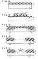
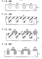
- the MOS LSI obtained in Example 1 could be extremely micro-sized to have a width of 1 ⁇ m because the field region 26 was determined by the width of groove 23, thus allowing the area of field regions in the LSI to be reduced and the high integration of LSI to be attained accordingly. If the field oxide film 6 having such a narrow width as shown in Fig. 5A was formed by the conventional selective oxidation method, the length (L) between elements was made short and the threshold voltage of parasitic field MOS transistor was reduced causing leak current to flow between elements. In contrast, the field region 26 of Example 1 was narrow in width as shown in Fig. 5B but had a full depth of 2 ⁇ m, for example, so that the channel length (L') between elements could be made long enough to prevent leak current from flowing between elements.
- the silicon substrate 21 was made flat having no stepped portion between the field region and the element forming region after the formation of field regions 26, as shown in Fig. 4E. Therefore, when At electrodes 33 and 34 were formed, disconnection of Ai electrodes at the regions between the field region and the element forming region could be prevented. Since p + -regions 24 which function as channel stopper regions were present under the bottom of grooves 23, they were not diffused into the element forming region, thus preventing the element property from being degraded due to narrow channel effect and the floating amount of n +- regions 29 and 30 from being increased because of contact between the p +- region 24 and the n +- regions 29, 30, which function as source and drain, respectively. Further, since field oxidation carried out in the selective oxidation method was made unnecessary, the occurrence of failure of silicon substrate due to stress caused at the time when the field oxide film would penetrate under the Si 3 N 4 film could be prevented.
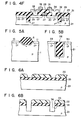
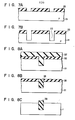
- grooves 23 are formed in the substrate 21 using the resist pattern 22 as a mask after the resist pattern 22 is formed directly on the silicon substrate 21 in Example 1, may be employed a process comprising depositing an insulating film 35 such as SiN film on the silicon substrate 21 as shown in Fig. 6A, then forming the resist pattern 22 thereon, etching the insulating film 35 by reactive ion etching using the resist pattern as the mask to form holes 36 therein, and further forming grooves 23 associated with holes 36 in the substrate 21 (Fig. 6B).
- the insulating film 35 on the silicon substrate 21 may be patterned as shown in Fig. 7A and reactive ion etching then be applied thereto using this insulating film as the mask to form grooves as shown in Fig. 7B.
- the insulating film 35 is then removed and Si0 2 is deposited on the whole surface of substrate 21 by the same process as shown in Fig. 4D. However, it is also possible to deposit Si0 2 without removing the insulating film 35.
- the groove is formed using the SiN film 35 as a mask, for example, and Si0 2 is then deposited to form an Si0 2 film 37, which fills the groove completely. Thereafter, the Si0 2 film 37 is etched, but it is not necessarily needed that- the film 37 is etched until the substrate 21 is exposed, and etching may be carried out until the SiN film 35 is exposed, as shown in Fig. 8B. And the SiN film 35 may be then etched as shown in Fig. 8C. An Si0 2 film 38 which is left in the groove at this time projects from the substrate 21, but this is often more advantageous because the surface of projected Si0 2 film 38 is etched in the subsequent process of using ammonium fluoride to thereby make its film thickness smaller.
- the insulating film 35 such as oxide film, for example, was deposited on the p-type silicon substrate 21 having crystal face (100), and the oxide film 35 was then patterned by photolithography (Fig. 9B).
- the silicon substrate 21 was etched by KO H using the oxide film pattern 35 as a mask.
- grooves 39 each having side faces sloped by an angle ⁇ and having a V-shaped cross section were formed.
- oxide film pattern 35 boron which is an impurity of same conductivity type as that of substrate 21 was ion-implanted under accelerating voltage of 50 keV and dose of 5 x 10 12 /cm 2 and heat treatment was then applied thereto to form p +- regions 40 under the bottom of grooves 39, respectively, said- p +- regions functioning as channel stopper regions (Fig. 9D).
- Si0 2 was deposited by CVD method on the whole surface thereof.
- the film thickness of Si0 2 deposited was larger than (a ⁇ cot ⁇ /2)/2 providing that the width of groove opening was denoted by "a”.
- Si0 2 was gradually deposited on the substrate 21 and the inner surface of grooves 40 and a CVD-Si0 2 film 41 was formed filling grooves 40 completely, as shown in Fig. 9E.
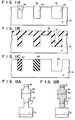
- Si0 2 film 41 The formation of Si0 2 film 41 will be described in more detail referring to Figs. 10A and 10B.
- the groove 40 becomes shallower gradually as the Si0 2 film is deposited to form its layers 41-1, 41-2, ... successively.
- the Si0 2 film is deposited thicker than a point 0 at which bisectors l and m of angles ⁇ which are formed by side faces of groove and the surface of substrate intersect each other, the groove 40 is completely filled with SiO 2 .
- a Providing that angles formed by bisectors l, m and a vertical line are represented by a, a equals to ⁇ /2. Therefore, the thickness of Si0 2 film at the point O is:
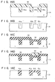
- a groove 49 whose opening width changed to be S l , S 2 , S 1 and S 3 was formed in the p-type silicon substrate 21 by photolithography in which reactive ion-etching was employed.
- the relation among S l , S 2 and S 3 was S l ⁇ S 2 ⁇ S 3 .
- Si0 2 was then deposited by CVD with a thickness a little larger than half the opening width (S 2 ) to completely fill the CVD-Si0 2 film in portions of groove 49 corresponding to its opening widths S 1 and S 2 and to leave the CVD-Si0 2 film deposited only on the inner surface of portion of groove 49 corresponding to its opening width S 3 .
- the CVD-Si0 2 film on the substrate 21 was etched by ammonium fluoride by the amount corresponding to the thickness of CVD-Si0 2 film.
- a field region 50 was obtained having portions S l and S 2 of groove 49 filled with the CVD-Si0 2 film and the portion S 3 of groove 49 from which CVD-Si0 2 film was removed.
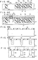
- the MOS LSI manufactured in this Example had narrow field region 66a and wide field region 73, and the silicon substrate 21 was made flat with no stepped portion formed between field regions and element forming region after the formation of field regions 66a and 73, as shown in Fig. 15I. Therefore, when At electrodes 80 and 81 were formed, such stepped portion as seen at the end of field region 54c in Example 5 was not caused and disconnection of metal electrode between field regions and element forming region could be prevented.
- p +- regions 64 and 71 which function as channel stopper regions, were arranged under the bottom of grooves 63a, 63b - 63e and 68a - 68c and therefore not diffused into the element forming region, thus preventing the element property from being degrade due to narrow channel effect and the floating capacity of n +- regions 76 and 77 from being increased due to the contact between p +- regions 64, 71 and n +- regions 76, 77, which function as source and drain. Further, the occurrence of leak current between elements could be prevented. Accordingly, a high quality and highly integrated MOS LSI could be obtained.
- Example 8 As described above, various disadvantages caused when the selective oxidation method was employed could be eliminated and a field insulating region having an optional width and no stepped portion could also be formed. Therefore, Example 8 could greatly contribute the manufacture of highly integrated and high quality LSI.
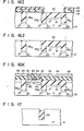
- oxide film 92 is formed integral with both field insulating films 86b and 86c. Instead, it may be separated from one or both of the films 86b and 86c.
Landscapes
- Element Separation (AREA)
Applications Claiming Priority (6)
| Application Number | Priority Date | Filing Date | Title |
|---|---|---|---|
| JP9722480A JPS5723240A (en) | 1980-07-16 | 1980-07-16 | Manufacture of semiconductor device |
| JP97223/80 | 1980-07-16 | ||
| JP97224/80 | 1980-07-16 | ||
| JP9722380A JPS5723239A (en) | 1980-07-16 | 1980-07-16 | Manufacture of semiconductor device |
| JP55168582A JPS5791535A (en) | 1980-11-29 | 1980-11-29 | Manufacture of semiconductor device |
| JP168582/80 | 1980-11-29 |
Related Child Applications (1)
| Application Number | Title | Priority Date | Filing Date |
|---|---|---|---|
| EP86116670.0 Division-Into | 1981-07-14 |
Publications (3)
| Publication Number | Publication Date |
|---|---|
| EP0044082A2 true EP0044082A2 (de) | 1982-01-20 |
| EP0044082A3 EP0044082A3 (en) | 1984-09-26 |
| EP0044082B1 EP0044082B1 (de) | 1989-03-22 |
Family
ID=27308349
Family Applications (2)
| Application Number | Title | Priority Date | Filing Date |
|---|---|---|---|
| EP86116670A Expired EP0245538B1 (de) | 1980-07-16 | 1981-07-14 | Verfahren zur Herstellung einer Halbleiteranordnung mit dielektrischen Isolationszonen |
| EP81105523A Expired EP0044082B1 (de) | 1980-07-16 | 1981-07-14 | Verfahren zur Herstellung einer Halbleiteranordnung mit einer dielektrischen isolierenden Zone |
Family Applications Before (1)
| Application Number | Title | Priority Date | Filing Date |
|---|---|---|---|
| EP86116670A Expired EP0245538B1 (de) | 1980-07-16 | 1981-07-14 | Verfahren zur Herstellung einer Halbleiteranordnung mit dielektrischen Isolationszonen |
Country Status (3)
| Country | Link |
|---|---|
| US (1) | US4394196A (de) |
| EP (2) | EP0245538B1 (de) |
| DE (2) | DE3177018D1 (de) |
Cited By (8)
| Publication number | Priority date | Publication date | Assignee | Title |
|---|---|---|---|---|
| DE3327301A1 (de) * | 1982-09-06 | 1984-03-08 | Hitachi, Ltd., Tokyo | Integrierte halbleiterschaltung und verfahren zu ihrer herstellung |
| EP0098687A3 (en) * | 1982-05-31 | 1985-09-18 | Kabushiki Kaisha Toshiba | Method of manufacturing a semiconductor device including burying an insulating film |
| EP0091507A3 (en) * | 1982-02-03 | 1986-04-16 | Kabushiki Kaisha Toshiba | Method of manufacturing a semi-conductor device comprising dielectric isolation regions |
| EP0098775B1 (de) * | 1982-07-01 | 1987-09-09 | Commissariat A L'energie Atomique | Verfahren zur Realisierung von einem Feldoxide für eine integrierte Schaltung |
| FR2598557A1 (fr) * | 1986-05-09 | 1987-11-13 | Seiko Epson Corp | Procede de fabrication d'une region d'isolation d'element d'un dispositif a semi-conducteurs |
| EP0137195B1 (de) * | 1983-10-13 | 1988-01-13 | International Business Machines Corporation | Dielektrisch isolierte Schaltung und Verfahren zur Herstellung |
| EP0242506A3 (en) * | 1986-03-17 | 1990-03-14 | International Business Machines Corporation | Sidewall spacers for cmos circuits stress relief/isolation and method for making |
| US4980311A (en) * | 1987-05-05 | 1990-12-25 | Seiko Epson Corporation | Method of fabricating a semiconductor device |
Families Citing this family (22)
| Publication number | Priority date | Publication date | Assignee | Title |
|---|---|---|---|---|
| DE3279874D1 (en) * | 1981-08-21 | 1989-09-14 | Toshiba Kk | Method of manufacturing dielectric isolation regions for a semiconductor device |
| US4563227A (en) * | 1981-12-08 | 1986-01-07 | Matsushita Electric Industrial Co., Ltd. | Method for manufacturing a semiconductor device |
| JPS58165341A (ja) * | 1982-03-26 | 1983-09-30 | Toshiba Corp | 半導体装置の製造方法 |
| JPS58171832A (ja) * | 1982-03-31 | 1983-10-08 | Toshiba Corp | 半導体装置の製造方法 |
| US4444605A (en) * | 1982-08-27 | 1984-04-24 | Texas Instruments Incorporated | Planar field oxide for semiconductor devices |
| US4609413A (en) * | 1983-11-18 | 1986-09-02 | Motorola, Inc. | Method for manufacturing and epitaxially isolated semiconductor utilizing etch and refill technique |
| US4456501A (en) * | 1983-12-22 | 1984-06-26 | Advanced Micro Devices, Inc. | Process for dislocation-free slot isolations in device fabrication |
| JPS6269520A (ja) * | 1985-09-21 | 1987-03-30 | Semiconductor Energy Lab Co Ltd | 光cvd法により凹部を充填する方法 |
| US5462767A (en) * | 1985-09-21 | 1995-10-31 | Semiconductor Energy Laboratory Co., Ltd. | CVD of conformal coatings over a depression using alkylmetal precursors |
| JPH0290617A (ja) * | 1988-09-28 | 1990-03-30 | Nec Corp | 半導体装置の製造方法 |
| JPH05109762A (ja) * | 1991-05-16 | 1993-04-30 | Internatl Business Mach Corp <Ibm> | 半導体装置及びその製造方法 |
| US5395790A (en) * | 1994-05-11 | 1995-03-07 | United Microelectronics Corp. | Stress-free isolation layer |
| US5374583A (en) * | 1994-05-24 | 1994-12-20 | United Microelectronic Corporation | Technology for local oxidation of silicon |
| US5577309A (en) * | 1995-03-01 | 1996-11-26 | Texas Instruments Incorporated | Method for forming electrical contact to the optical coating of an infrared detector |
| KR0147630B1 (ko) * | 1995-04-21 | 1998-11-02 | 김광호 | 반도체 장치의 소자분리방법 |
| US5725739A (en) | 1996-07-08 | 1998-03-10 | Micron Technology, Inc. | Low angle, low energy physical vapor deposition of alloys |
| JP3417767B2 (ja) * | 1996-08-29 | 2003-06-16 | 株式会社東芝 | 単結晶部品の製造方法 |
| US6333274B2 (en) | 1998-03-31 | 2001-12-25 | Kabushiki Kaisha Toshiba | Method of manufacturing a semiconductor device including a seamless shallow trench isolation step |
| US6265282B1 (en) * | 1998-08-17 | 2001-07-24 | Micron Technology, Inc. | Process for making an isolation structure |
| JP2005008909A (ja) * | 2003-06-16 | 2005-01-13 | Canon Inc | 構造体の製造方法 |
| KR101575818B1 (ko) * | 2009-08-18 | 2015-12-08 | 삼성전자주식회사 | 활성 영역 구조물의 형성방법 |
| US8633077B2 (en) | 2012-02-15 | 2014-01-21 | International Business Machines Corporation | Transistors with uniaxial stress channels |
Family Cites Families (14)
| Publication number | Priority date | Publication date | Assignee | Title |
|---|---|---|---|---|
| GB1461943A (en) * | 1973-02-21 | 1977-01-19 | Raytheon Co | Semi-conductor devices |
| US4032373A (en) * | 1975-10-01 | 1977-06-28 | Ncr Corporation | Method of manufacturing dielectrically isolated semiconductive device |
| US4104086A (en) * | 1977-08-15 | 1978-08-01 | International Business Machines Corporation | Method for forming isolated regions of silicon utilizing reactive ion etching |
| US4139442A (en) * | 1977-09-13 | 1979-02-13 | International Business Machines Corporation | Reactive ion etching method for producing deep dielectric isolation in silicon |
| US4140558A (en) * | 1978-03-02 | 1979-02-20 | Bell Telephone Laboratories, Incorporated | Isolation of integrated circuits utilizing selective etching and diffusion |
| US4264382A (en) * | 1978-05-25 | 1981-04-28 | International Business Machines Corporation | Method for making a lateral PNP or NPN with a high gain utilizing reactive ion etching of buried high conductivity regions |
| US4209349A (en) * | 1978-11-03 | 1980-06-24 | International Business Machines Corporation | Method for forming a narrow dimensioned mask opening on a silicon body utilizing reactive ion etching |
| US4209350A (en) * | 1978-11-03 | 1980-06-24 | International Business Machines Corporation | Method for forming diffusions having narrow dimensions utilizing reactive ion etching |
| US4255207A (en) * | 1979-04-09 | 1981-03-10 | Harris Corporation | Fabrication of isolated regions for use in self-aligning device process utilizing selective oxidation |
| US4211582A (en) * | 1979-06-28 | 1980-07-08 | International Business Machines Corporation | Process for making large area isolation trenches utilizing a two-step selective etching technique |
| US4252582A (en) * | 1980-01-25 | 1981-02-24 | International Business Machines Corporation | Self aligned method for making bipolar transistor having minimum base to emitter contact spacing |
| US4318751A (en) * | 1980-03-13 | 1982-03-09 | International Business Machines Corporation | Self-aligned process for providing an improved high performance bipolar transistor |
| US4274909A (en) * | 1980-03-17 | 1981-06-23 | International Business Machines Corporation | Method for forming ultra fine deep dielectric isolation |
| US4307180A (en) * | 1980-08-22 | 1981-12-22 | International Business Machines Corp. | Process of forming recessed dielectric regions in a monocrystalline silicon substrate |
-
1981
- 1981-07-13 US US06/282,642 patent/US4394196A/en not_active Expired - Lifetime
- 1981-07-14 DE DE8181105523T patent/DE3177018D1/de not_active Expired
- 1981-07-14 DE DE8686116670T patent/DE3177250D1/de not_active Expired - Lifetime
- 1981-07-14 EP EP86116670A patent/EP0245538B1/de not_active Expired
- 1981-07-14 EP EP81105523A patent/EP0044082B1/de not_active Expired
Cited By (12)
| Publication number | Priority date | Publication date | Assignee | Title |
|---|---|---|---|---|
| EP0091507A3 (en) * | 1982-02-03 | 1986-04-16 | Kabushiki Kaisha Toshiba | Method of manufacturing a semi-conductor device comprising dielectric isolation regions |
| EP0098687A3 (en) * | 1982-05-31 | 1985-09-18 | Kabushiki Kaisha Toshiba | Method of manufacturing a semiconductor device including burying an insulating film |
| EP0098775B1 (de) * | 1982-07-01 | 1987-09-09 | Commissariat A L'energie Atomique | Verfahren zur Realisierung von einem Feldoxide für eine integrierte Schaltung |
| DE3327301A1 (de) * | 1982-09-06 | 1984-03-08 | Hitachi, Ltd., Tokyo | Integrierte halbleiterschaltung und verfahren zu ihrer herstellung |
| US4746963A (en) * | 1982-09-06 | 1988-05-24 | Hitachi, Ltd. | Isolation regions formed by locos followed with groove etch and refill |
| US5084402A (en) * | 1982-09-06 | 1992-01-28 | Hitachi, Ind. | Method of fabricating a semiconductor substrate, and semiconductor device, having thick oxide films and groove isolation |
| EP0137195B1 (de) * | 1983-10-13 | 1988-01-13 | International Business Machines Corporation | Dielektrisch isolierte Schaltung und Verfahren zur Herstellung |
| EP0242506A3 (en) * | 1986-03-17 | 1990-03-14 | International Business Machines Corporation | Sidewall spacers for cmos circuits stress relief/isolation and method for making |
| FR2598557A1 (fr) * | 1986-05-09 | 1987-11-13 | Seiko Epson Corp | Procede de fabrication d'une region d'isolation d'element d'un dispositif a semi-conducteurs |
| NL8701087A (nl) * | 1986-05-09 | 1987-12-01 | Seiko Epson Corp | Werkwijze voor het vervaardigen van een half-geleiderinrichting. |
| GB2190241B (en) * | 1986-05-09 | 1989-12-13 | Seiko Epson Corp | Method of making a semiconductor device |
| US4980311A (en) * | 1987-05-05 | 1990-12-25 | Seiko Epson Corporation | Method of fabricating a semiconductor device |
Also Published As
| Publication number | Publication date |
|---|---|
| EP0245538A3 (en) | 1988-02-17 |
| DE3177250D1 (de) | 1991-08-14 |
| EP0044082B1 (de) | 1989-03-22 |
| EP0245538A2 (de) | 1987-11-19 |
| EP0245538B1 (de) | 1991-07-10 |
| EP0044082A3 (en) | 1984-09-26 |
| US4394196A (en) | 1983-07-19 |
| DE3177018D1 (en) | 1989-04-27 |
Similar Documents
| Publication | Publication Date | Title |
|---|---|---|
| EP0044082B1 (de) | Verfahren zur Herstellung einer Halbleiteranordnung mit einer dielektrischen isolierenden Zone | |
| EP0061855B1 (de) | Verfahren zur Herstellung eines Halbleiterbauelements | |
| US5316965A (en) | Method of decreasing the field oxide etch rate in isolation technology | |
| JP2512216B2 (ja) | 半導体装置の製造方法 | |
| EP0631307B1 (de) | Verfahren zur Herstellung einer Halbleiteranordnung mit Grabenstruktur für Element Isolationszonen | |
| US4419813A (en) | Method for fabricating semiconductor device | |
| US4491486A (en) | Method for manufacturing a semiconductor device | |
| JPS61133623A (ja) | 分離溝側壁への注入方法 | |
| US4532696A (en) | Method of manufacturing a semiconductor device for forming a deep field region in a semiconductor substrate | |
| US6103574A (en) | Method of manufacturing non-volatile semiconductor memory device having reduced electrical resistance of a source diffusion layer | |
| EP0091507A2 (de) | Verfahren zur Herstellung einer Halbleiteranordnung mit dielektrischen Isolationszonen | |
| EP0160965B1 (de) | Verfahren zum Herstellen einer Halbleiteranordnung mit einer Gateelektrodenstapel-Struktur | |
| JPS6355780B2 (de) | ||
| US5147818A (en) | Method for manufacturing a BiCMOS semiconductor device having a lateral bipolar transistor | |
| US5705440A (en) | Methods of fabricating integrated circuit field effect transistors having reduced-area device isolation regions | |
| US5221857A (en) | Bipolar transistor structure with polycrystalline resistor layer | |
| EP0412263B1 (de) | Verfahren zum Herstellen eines kontaktloches in einem integrierten Halbleiterstromkreis | |
| JPH08274166A (ja) | 半導体装置及びその製造方法 | |
| US6080625A (en) | Method for making dual-polysilicon structures in integrated circuits | |
| JPS6119111B2 (de) | ||
| JPS6251216A (ja) | 半導体装置の製造方法 | |
| JP3288211B2 (ja) | 半導体装置の製造方法 | |
| JP2565744B2 (ja) | Cmos集積回路装置の製造方法 | |
| JPH0363220B2 (de) | ||
| JPS5986263A (ja) | 半導体装置の製造方法 |
Legal Events
| Date | Code | Title | Description |
|---|---|---|---|
| PUAI | Public reference made under article 153(3) epc to a published international application that has entered the european phase |
Free format text: ORIGINAL CODE: 0009012 |
|
| AK | Designated contracting states |
Designated state(s): DE FR GB NL |
|
| 17P | Request for examination filed |
Effective date: 19820215 |
|
| PUAL | Search report despatched |
Free format text: ORIGINAL CODE: 0009013 |
|
| RAP1 | Party data changed (applicant data changed or rights of an application transferred) |
Owner name: KABUSHIKI KAISHA TOSHIBA |
|
| AK | Designated contracting states |
Designated state(s): DE FR GB NL |
|
| 17Q | First examination report despatched |
Effective date: 19860122 |
|
| R17C | First examination report despatched (corrected) |
Effective date: 19860723 |
|
| GRAA | (expected) grant |
Free format text: ORIGINAL CODE: 0009210 |
|
| AK | Designated contracting states |
Kind code of ref document: B1 Designated state(s): DE FR GB NL |
|
| REF | Corresponds to: |
Ref document number: 3177018 Country of ref document: DE Date of ref document: 19890427 |
|
| ET | Fr: translation filed | ||
| PLBE | No opposition filed within time limit |
Free format text: ORIGINAL CODE: 0009261 |
|
| STAA | Information on the status of an ep patent application or granted ep patent |
Free format text: STATUS: NO OPPOSITION FILED WITHIN TIME LIMIT |
|
| 26N | No opposition filed | ||
| REG | Reference to a national code |
Ref country code: GB Ref legal event code: 746 Effective date: 19981015 |
|
| REG | Reference to a national code |
Ref country code: FR Ref legal event code: D6 |
|
| PGFP | Annual fee paid to national office [announced via postgrant information from national office to epo] |
Ref country code: DE Payment date: 20000710 Year of fee payment: 20 |
|
| PGFP | Annual fee paid to national office [announced via postgrant information from national office to epo] |
Ref country code: FR Payment date: 20000711 Year of fee payment: 20 |
|
| PGFP | Annual fee paid to national office [announced via postgrant information from national office to epo] |
Ref country code: GB Payment date: 20000713 Year of fee payment: 20 |
|
| PGFP | Annual fee paid to national office [announced via postgrant information from national office to epo] |
Ref country code: NL Payment date: 20000728 Year of fee payment: 20 |
|
| PG25 | Lapsed in a contracting state [announced via postgrant information from national office to epo] |
Ref country code: GB Free format text: LAPSE BECAUSE OF EXPIRATION OF PROTECTION Effective date: 20010713 |
|
| PG25 | Lapsed in a contracting state [announced via postgrant information from national office to epo] |
Ref country code: NL Free format text: LAPSE BECAUSE OF EXPIRATION OF PROTECTION Effective date: 20010714 |
|
| REG | Reference to a national code |
Ref country code: GB Ref legal event code: PE20 Effective date: 20010713 |
|
| NLV7 | Nl: ceased due to reaching the maximum lifetime of a patent |
Effective date: 20010714 |