EP0045046A1 - Halbleiterbauelement und seine Verwendung für statische 6-Transistorzelle - Google Patents
Halbleiterbauelement und seine Verwendung für statische 6-Transistorzelle Download PDFInfo
- Publication number
- EP0045046A1 EP0045046A1 EP81105754A EP81105754A EP0045046A1 EP 0045046 A1 EP0045046 A1 EP 0045046A1 EP 81105754 A EP81105754 A EP 81105754A EP 81105754 A EP81105754 A EP 81105754A EP 0045046 A1 EP0045046 A1 EP 0045046A1
- Authority
- EP
- European Patent Office
- Prior art keywords
- field
- insulating layer
- effect transistor
- transistor
- source
- Prior art date
- Legal status (The legal status is an assumption and is not a legal conclusion. Google has not performed a legal analysis and makes no representation as to the accuracy of the status listed.)
- Granted
Links
Images


Classifications
-
- H—ELECTRICITY
- H10—SEMICONDUCTOR DEVICES; ELECTRIC SOLID-STATE DEVICES NOT OTHERWISE PROVIDED FOR
- H10B—ELECTRONIC MEMORY DEVICES
- H10B10/00—Static random access memory [SRAM] devices
- H10B10/12—Static random access memory [SRAM] devices comprising a MOSFET load element
-
- H—ELECTRICITY
- H10—SEMICONDUCTOR DEVICES; ELECTRIC SOLID-STATE DEVICES NOT OTHERWISE PROVIDED FOR
- H10B—ELECTRONIC MEMORY DEVICES
- H10B10/00—Static random access memory [SRAM] devices
- H10B10/12—Static random access memory [SRAM] devices comprising a MOSFET load element
- H10B10/125—Static random access memory [SRAM] devices comprising a MOSFET load element the MOSFET being a thin film transistor [TFT]
-
- H—ELECTRICITY
- H10—SEMICONDUCTOR DEVICES; ELECTRIC SOLID-STATE DEVICES NOT OTHERWISE PROVIDED FOR
- H10D—INORGANIC ELECTRIC SEMICONDUCTOR DEVICES
- H10D84/00—Integrated devices formed in or on semiconductor substrates that comprise only semiconducting layers, e.g. on Si wafers or on GaAs-on-Si wafers
- H10D84/80—Integrated devices formed in or on semiconductor substrates that comprise only semiconducting layers, e.g. on Si wafers or on GaAs-on-Si wafers characterised by the integration of at least one component covered by groups H10D12/00 or H10D30/00, e.g. integration of IGFETs
- H10D84/82—Integrated devices formed in or on semiconductor substrates that comprise only semiconducting layers, e.g. on Si wafers or on GaAs-on-Si wafers characterised by the integration of at least one component covered by groups H10D12/00 or H10D30/00, e.g. integration of IGFETs of only field-effect components
- H10D84/83—Integrated devices formed in or on semiconductor substrates that comprise only semiconducting layers, e.g. on Si wafers or on GaAs-on-Si wafers characterised by the integration of at least one component covered by groups H10D12/00 or H10D30/00, e.g. integration of IGFETs of only field-effect components of only insulated-gate FETs [IGFET]
- H10D84/8311—Integrated devices formed in or on semiconductor substrates that comprise only semiconducting layers, e.g. on Si wafers or on GaAs-on-Si wafers characterised by the integration of at least one component covered by groups H10D12/00 or H10D30/00, e.g. integration of IGFETs of only field-effect components of only insulated-gate FETs [IGFET] the IGFETs characterised by having different channel structures
-
- H—ELECTRICITY
- H10—SEMICONDUCTOR DEVICES; ELECTRIC SOLID-STATE DEVICES NOT OTHERWISE PROVIDED FOR
- H10D—INORGANIC ELECTRIC SEMICONDUCTOR DEVICES
- H10D84/00—Integrated devices formed in or on semiconductor substrates that comprise only semiconducting layers, e.g. on Si wafers or on GaAs-on-Si wafers
- H10D84/80—Integrated devices formed in or on semiconductor substrates that comprise only semiconducting layers, e.g. on Si wafers or on GaAs-on-Si wafers characterised by the integration of at least one component covered by groups H10D12/00 or H10D30/00, e.g. integration of IGFETs
- H10D84/82—Integrated devices formed in or on semiconductor substrates that comprise only semiconducting layers, e.g. on Si wafers or on GaAs-on-Si wafers characterised by the integration of at least one component covered by groups H10D12/00 or H10D30/00, e.g. integration of IGFETs of only field-effect components
- H10D84/83—Integrated devices formed in or on semiconductor substrates that comprise only semiconducting layers, e.g. on Si wafers or on GaAs-on-Si wafers characterised by the integration of at least one component covered by groups H10D12/00 or H10D30/00, e.g. integration of IGFETs of only field-effect components of only insulated-gate FETs [IGFET]
- H10D84/8312—Integrated devices formed in or on semiconductor substrates that comprise only semiconducting layers, e.g. on Si wafers or on GaAs-on-Si wafers characterised by the integration of at least one component covered by groups H10D12/00 or H10D30/00, e.g. integration of IGFETs of only field-effect components of only insulated-gate FETs [IGFET] the IGFETs characterised by having different source or drain region structures, e.g. IGFETs having symmetrical source or drain regions integrated with IGFETs having asymmetrical source or drain regions
-
- H—ELECTRICITY
- H10—SEMICONDUCTOR DEVICES; ELECTRIC SOLID-STATE DEVICES NOT OTHERWISE PROVIDED FOR
- H10D—INORGANIC ELECTRIC SEMICONDUCTOR DEVICES
- H10D88/00—Three-dimensional [3D] integrated devices
Definitions
- the invention relates to a semiconductor component with at least two field effect transistors, in which source and drain regions of a first and second field effect transistors designed as insulating layer field effect transistors are arranged in a doped semiconductor body covered by an electrically insulating layer, the gate of one field effect transistor. transistor on the insulating layer also forms the source or drain region of the other field effect transistor.
- Such a semiconductor device is known from DE-OS 25 03 846.
- the doping regions in a semiconductor body are used several times for the construction of the individual field-effect transistors, a semiconductor area being used for the configuration with two insulating-layer field-effect transistors, which is smaller by the partial area falling on a source or drain region of the transistor than in one Construction of two field effect transistors built independently of each other.
- the invention is based on the object of using this principle of the reduced space requirement for highly integrated, static semiconductor memories 9, in particular for the switching transistors of a 6-transistor cell.
- a static 6-transistor cell can be found, for example, in the book "Semiconductor Memory Design and Application” by Luecke, Mize, Carr, Mac Graw-Hill, Kogakusha, Ltd., Figure 5.3, p. 118.
- a semiconductor component of the type mentioned at the outset is proposed, which is characterized over the prior art in that the gate of the first field effect transistor made of polysilicon is converted by region-wise conversion of polysilicon into the single-crystal structure also forms the drain and / or source region of the second transistor.
- a plurality of double layers on the single-crystalline silicon layer produced by region-wise conversion of polysilicon; consisting in each case of a further insulating layer and a further layer covering this region-converted polysilicon in the single-crystalline structure, and that in each of the further layers of region-converted monocrystalline silicon a region is provided which the source and / or Forms the drain region of a further field effect transistor, the gate, drain and / or source region of which is located in other layers of regionally converted single-crystal silicon.
- the single-crystalline silicon region is generated by laser or electron radiation.
- laser or electron radiation As is known from EF Krimmel, Semiconductor Device University Bulletin Meeting, CNR - LAIIEL, Bologna, June 15, 1979 and AF Tasch jun., TC Holloway, KF Lee, JF Gibbons, "Electronics Letters 15, 435 - 437, (1979), Is it possible, with the help of laser or electron beam healing to make polycrystalline silicon applied to amorphous Si0 2 in some areas and to produce functional transistors in these areas. This results in the possibility of combining the switching transistors of the 6-transistor cell in a way not previously known and thereby saving considerably on the silicon surface.
- S 1, S 2, S 3, S 4, S 5 and S 6 are the source regions, with D 1, D 2, D 3, D4, D5 and D6 the Drainbere i che and G 1, G 2, G 3 , G 4 , G 5 and G 6 marked the gate areas.
- 10 denotes the first insulating layer covering the semiconductor body 11 and consisting of SiO 2
- 12 denotes the second insulating layer.
- FIG. 7 shows a circuit diagram of a 6-transistor RAM cell which can be easily implemented using the semiconductor component constructed according to the invention.
- V DD is the operating voltage and V SS the operating voltage zero, 14 and 15 the bit lines A and B and 16 the word line.
- FIG. 1 and 2 The transistor 1 is in a known manner produced. However, the polycrystalline silicon gate G 1 of this transistor (S 1 D 1 G 1 ) continues in the lateral direction and is made single-crystalline according to the invention by laser or electron beam healing and a second transistor (D 2 G 2 S 2 ) is produced in this area, whereby the drain D 2 of transistor 2 also serves as gate G 1 of transistor 1.
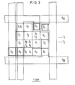
- FIG. 3 The further development can be seen in FIG. 3.
- the dashed line circumscribes transistor 1, the dash-dotted line transistor 2.
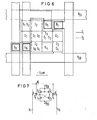
- FIGS. 4 and 5 A further space saving results if the two switching transistors are placed one above the other in a cross shape.
- the lateral extension of the gate G 1 of the transistor 1 is the drain D 2 and the source S 2 region of the transistor 2.
- the current-carrying transistor is conductive in the regions in which the Potential of the blocked transistor is above the threshold voltage. If complete switching of the current-carrying transistor is to be achieved, a doping gradient of the transistors from source to drain must be established, which can be done, for example, by ion implantation using a beveled oxide as an implantation mask.
- FIGS. 4 and 5 can be seen from the layout shown in FIG. 6 in an analogous manner to that in FIG. 3.
- the area is 20 x 25 / um 2 corresponds to 500 / um 2 . Otherwise the same reference numerals apply as in FIG. 3.
Landscapes
- Thin Film Transistor (AREA)
- Recrystallisation Techniques (AREA)
- Semiconductor Integrated Circuits (AREA)
- Metal-Oxide And Bipolar Metal-Oxide Semiconductor Integrated Circuits (AREA)
- Semiconductor Memories (AREA)
Abstract
Description
- Die Erfindung bezieht sich auf ein Halbleiterbauelement mit mindestens zwei Feldeffekttransistoren, bei dem in einem von einer elektrisch isolierenden Schicht bedeckten, dotierten Halbleiterkörper Source- und Draingebiete eines ersten und zweiten, als Isolierschicht-Feldeffekttransistoren ausgebildete Feldeffekttransistoren angeordnet sind, wobei das Gate des einen Feldeffekt- transistors auf der isolierenden Schicht zugleich das Source- oder Draingebiet des anderen Feldeffekttransistors bildet.
- Ein solches Halbleiterbauelement ist aus der DE-OS 25 03 846 bekannt. Bei diesem Bauelement werden die Dotierungsbereiche in einem Halbleiterkörper für den Aufbau der einzelnen Feldeffekttransistoren mehrfach ausgenutzt, wobei eine Halbleiterfläche für die Ausgestaltung mit zwei Isolierschicht-Feldeffekttransistoren beansprucht wird, die um die auf ein Source- oder Draingebiet des Transistors fallende Teilfläche kleiner ist als bei einem Aufbau von zwei unabhängig voneinander aufgebauten Feldeffekttransistoren.
- Der Erfindung liegt die Aufgabe zugrunde, dieses Prinzip des verringerten Platzbedarfes für hochintegrierte, statische Halbleiterspeicher9 insbesondere für die Schalttransistoren einer 6-Transistorzelle zu verwenden. Eine solche statische 6-Transistorzelle ist beispielsweise aus dem Buch "Semiconductor Memory Design and Application" von Luecke, Mize, Carr, Mac Graw-Hill, Kogakusha, Ltd., Figur 5.3, S. 118 zu entnehmen.
- Trotz der vielen Vorteile, die eine statische Speicherzelle bietet, hat sich bislang aus Flächenbedarfsgründen-die 6-Transistorzelle benötigt ca. 2000 bis 2500 /um2 in der 5 /um-Technologie - die flächengünstigere 1-Transistorzelle durchgesetzt, die jedoch dynamisch betrieben werden muß.
- Zur Lösung der Aufgabe, mit verringertem Platzbedarf eine statische 6-Transistorzelle zu realisieren, wird ein Halbleiterbauelement der eingangs genannten Art vorgeschlagen, welches gegenüber dem Stand der Technik dadurch gekennzeichnet ist, daß das aus Polysilizium bestehende Gate des ersten Feldeffekttransistors durch bereichsweise Umwandlung von Polysilizium in die einkristalline Struktur zugleich das Drain und/oder Source-Gebiet des zweiten Transistors bildet. Dabei liegt es im Rahmen der Erfindung, daß auf der durch bereichsweise Umwandlung von Polysilizium erzeugten einkristallinen Siliziumschicht mehrere Doppelschichten; jeweils bestehend aus einer weiteren isolierenden Schicht und einer weiteren, diese bedeckende Schicht aus bereichsweise umgewandelten Polysilizium in die einkristalline Struktur, aufgebracht sind und daß in jeder der weiteren Schichten aus bereichsweise umgewandelten einkristallinem Silizium ein Bereich vorgesehen ist, der das Source- und/oder das Draingebiet eines weiteren Feldeffekttransistors bildet, dessen Gate, Drain- und/oder Sourcebereich sich in anderen Schichten aus bereichsweise umgewandelten einkristallinen Silizium befindet.
- In einer Weiterbildung des Erfindungsgedankens ist vorgesehen, daß das einkristalline Siliziumgebiet durch Laser-oder Elektronenbestrahlung erzeugt ist. Wie aus E.F. Krimmel, Semiconductor Device University Bulletin Meeting, C. N. R. - LAIIEL, Bologna, 15.6.1979 und A. F. Tasch jun., T. C. Holloway, K. F. Lee, J. F. Gibbons, "Electronics Letters 15, 435 - 437, (1979) bekannt ist, ist es möglich, mit Hilfe der Laser- oder Elektronenstrahlausheilung auf amorphem Si02 aufgebrachtes polykristallines Silizium bereichsweise einkristallin zu machen und in diesen Bereichen funktionsfähige Transistoren herzustellen. Hierdurch ergibt sich die Möglichkeit, die Schalttransistoren der 6-Transistorzelle in bisher nicht gekannter Weise zu kombinieren und dadurch wesentlich an Silizium-Oberfläche einzusparen.
- Besonders vorteilhafte Weiterbildungen der Erfindung ergeben sich aus den Unteransprüchen, sowie aus den in der Zeichnung befindlichen Figuren 1 bis 7. Dabei zeigen
- die Figuren 1 bis 3 die Anordnung der Feldeffekttransistoren im Halbleiterkörper in T-Struktur-Gate-Stapelform (Gäte-Stack), wobei die Figur 3 ein vollständiges Layout einer 6-Transistorzelle zeigt, während
- die Figuren 4 bis 6 ein analoges Ausführungsbeispiel in Kreuz-Struktur-Gate-Stapelform (Gate-Stack) darstellen.
- Mit S1, S2, S3, S4, S5 und S6 sind die Sourcebereiche, mit D1, D2, D3, D4, D5 und D6 die Drainbereiche und mit G 1, G2, G3, G4, G5 und G6 die Gatebereiche gekennzeichnet. Mit 10 ist die den Halbleiterkörper 11 bedeckende, aus Si02 bestehende erste Isolierschicht, mit 12 die zweite Isolierschicht bezeichnet. In Figur 7 ist ein Schaltbild einer 6-Transistor-RAM-Zelle angegeben, die mit dem nach der Erfindung aufgebauten Halbleiterbauelement leicht realisiert werden kann. Dabei sind mit VDD die Betriebsspannung und VSS der Betriebsspannungsnullpunkt, mit 14 und 15 die Bitleitung A und B und mit 16 die Wortleitung gekennzeichnet.
- Figur 1 und 2: Der Transistor 1 wird in bekannter Weise hergestellt. Das polykristalline Siliziumgate G1 dieses Transistors (S1D1G1) setzt sich jedoch in lateraler Richtung fort und wird erfindungsgemäß durch Laser- oder Elektronenstrahlausheilung einkristallin gemacht und auf diesem Gebiet ein zweiter Transistor (D2G2S2) hergestellt, wobei das Drain D2 von Transistor 2 gleichzeitig als Gate G1 von Transistor 1 dient.
- Die Weiterbildung ist aus Figur 3 ersichtlich. Die Fläche beträgt 25 x 25 = 625 /um . Die gestrichelte Linie umschreibt den Transistor 1, die strichpunktierte den Transistor 2.
- Figur 4 und 5: Eine weitere Platzersparnis ergibt sich, wenn die beiden Schalttransistoren kreuzförmig übereinandergelegt werden. Dabei ist, wie aus Figur 4 und 5 ersichtlich, die laterale Ausdehnung des Gate G1 des Transistors 1 das Drain D2- und das Source S2-Gebiet vom Transistor 2. Hierbei ist der stromführende Transistor in den Bereichen leitend, in denen das Potential des gesperrten Transistors über der Einsatzspannung liegt. Soll ein vollständiges Durchschalten des stromführenden Transistors erreicht werden, so muß ein Dotierungsgradient der Transistoren von Source nach Drain hergestellt werden, was beispielsweise durch Ionenimplantation durch ein abgeschrägtes Oxid als Implantationsmaske erfolgen kann.
- Die Weiterbildung von Figur 4 und 5 ist aus dem in Figur 6 dargestellten Layout in analoger Weise wie in Figur 3 ersichtlich. Die Fläche beträgt 20 x 25 /um2 ent- spricht 500 /um2. Im übrigen gelten die gleichen Bezugszeichen wie in Figur 3.
Claims (6)
Applications Claiming Priority (2)
| Application Number | Priority Date | Filing Date | Title |
|---|---|---|---|
| DE19803028111 DE3028111A1 (de) | 1980-07-24 | 1980-07-24 | Halbleiterbauelement und seine verwendung fuer statische 6-transistorzelle |
| DE3028111 | 1980-07-24 |
Publications (2)
| Publication Number | Publication Date |
|---|---|
| EP0045046A1 true EP0045046A1 (de) | 1982-02-03 |
| EP0045046B1 EP0045046B1 (de) | 1984-10-24 |
Family
ID=6108033
Family Applications (1)
| Application Number | Title | Priority Date | Filing Date |
|---|---|---|---|
| EP81105754A Expired EP0045046B1 (de) | 1980-07-24 | 1981-07-21 | Halbleiterbauelement und seine Verwendung für statische 6-Transistorzelle |
Country Status (3)
| Country | Link |
|---|---|
| EP (1) | EP0045046B1 (de) |
| JP (1) | JPS5753972A (de) |
| DE (1) | DE3028111A1 (de) |
Cited By (5)
| Publication number | Priority date | Publication date | Assignee | Title |
|---|---|---|---|---|
| EP0104616A3 (de) * | 1982-09-28 | 1986-01-15 | Siemens Aktiengesellschaft | Statische Speicherzelle in Zwei-Kanal-Technik |
| US4570175A (en) * | 1982-06-22 | 1986-02-11 | Hitachi, Ltd. | Three-dimensional semiconductor device with thin film monocrystalline member contacting substrate at a plurality of locations |
| GB2224160A (en) * | 1988-10-24 | 1990-04-25 | Marconi Instruments Ltd | Integrated semiconductor circuits |
| EP0392540A3 (de) * | 1989-04-14 | 1991-04-03 | Kabushiki Kaisha Toshiba | Statischer Speicher |
| EP1586108A4 (de) * | 2002-12-19 | 2009-03-04 | Ibm | Finfet sram-zelle mit invertierten finfet-dünnschichttransistoren |
Families Citing this family (4)
| Publication number | Priority date | Publication date | Assignee | Title |
|---|---|---|---|---|
| JPS5939061A (ja) * | 1982-08-27 | 1984-03-03 | Hitachi Ltd | 半導体装置 |
| JPS59130459A (ja) * | 1983-01-17 | 1984-07-27 | Hitachi Ltd | 半導体メモリ集積回路装置 |
| JPS61222254A (ja) * | 1985-03-28 | 1986-10-02 | Toshiba Corp | 半導体記憶装置 |
| JP4190311B2 (ja) * | 2003-03-10 | 2008-12-03 | 三菱電機株式会社 | 半導体装置 |
Citations (2)
| Publication number | Priority date | Publication date | Assignee | Title |
|---|---|---|---|---|
| US3585088A (en) * | 1968-10-18 | 1971-06-15 | Ibm | Methods of producing single crystals on supporting substrates |
| DE2503864A1 (de) * | 1975-01-30 | 1976-08-05 | Siemens Ag | Halbleiterbauelement |
Family Cites Families (1)
| Publication number | Priority date | Publication date | Assignee | Title |
|---|---|---|---|---|
| JPS503787A (de) * | 1973-05-16 | 1975-01-16 |
-
1980
- 1980-07-24 DE DE19803028111 patent/DE3028111A1/de not_active Ceased
-
1981
- 1981-07-21 EP EP81105754A patent/EP0045046B1/de not_active Expired
- 1981-07-23 JP JP56115838A patent/JPS5753972A/ja active Pending
Patent Citations (2)
| Publication number | Priority date | Publication date | Assignee | Title |
|---|---|---|---|---|
| US3585088A (en) * | 1968-10-18 | 1971-06-15 | Ibm | Methods of producing single crystals on supporting substrates |
| DE2503864A1 (de) * | 1975-01-30 | 1976-08-05 | Siemens Ag | Halbleiterbauelement |
Cited By (5)
| Publication number | Priority date | Publication date | Assignee | Title |
|---|---|---|---|---|
| US4570175A (en) * | 1982-06-22 | 1986-02-11 | Hitachi, Ltd. | Three-dimensional semiconductor device with thin film monocrystalline member contacting substrate at a plurality of locations |
| EP0104616A3 (de) * | 1982-09-28 | 1986-01-15 | Siemens Aktiengesellschaft | Statische Speicherzelle in Zwei-Kanal-Technik |
| GB2224160A (en) * | 1988-10-24 | 1990-04-25 | Marconi Instruments Ltd | Integrated semiconductor circuits |
| EP0392540A3 (de) * | 1989-04-14 | 1991-04-03 | Kabushiki Kaisha Toshiba | Statischer Speicher |
| EP1586108A4 (de) * | 2002-12-19 | 2009-03-04 | Ibm | Finfet sram-zelle mit invertierten finfet-dünnschichttransistoren |
Also Published As
| Publication number | Publication date |
|---|---|
| DE3028111A1 (de) | 1982-02-18 |
| EP0045046B1 (de) | 1984-10-24 |
| JPS5753972A (de) | 1982-03-31 |
Similar Documents
| Publication | Publication Date | Title |
|---|---|---|
| DE102013105074B4 (de) | Integrierter Schaltkreis, der FinFETs mit verschiedenen Finnenprofilen umfasst | |
| DE102013104983B4 (de) | Zellen-Layout für SRAM-FinFET-Transistoren | |
| DE69224453T2 (de) | Verfahren zur Herstellung von einem LDD-MOSFET | |
| DE1589810C3 (de) | Passiviertes Halbleiterbauelement und Verfahren zu seiner Herstellung | |
| DE69226405T2 (de) | Geschichtete CMOS SRAM Zelle mit polysilizium-Lasttransistoren | |
| DE3029125C2 (de) | Halbleiterspeicher | |
| EP0000327B1 (de) | Verfahren zum Herstellen von integrierten Halbleiteranordnungen durch Anwendung einer auf Selbstausrichtung basierenden Maskierungstechnik | |
| DE3873839T2 (de) | Mos-leistungstransistoranordnung. | |
| DE69133300T2 (de) | Feldeffektanordnung mit einem Kanal aus polykristallinem Silizium | |
| DE2728167A1 (de) | Verfahren zur vorbereitung eines siliziumsubstrats fuer die herstellung von mos-bauelementen | |
| DE2750209A1 (de) | Integrierte halbleiterschaltung und verfahren zu ihrer herstellung | |
| DE3037431A1 (de) | Verfahren zur herstellung von elektrisch programmierbaren festwertspeichern in mos-technologie | |
| DE2911132A1 (de) | Verfahren zur bildung einer kontaktzone zwischen schichten aus polysilizium | |
| DE3787687T2 (de) | Halbleiterspeicher. | |
| EP0168528B1 (de) | Ein-Transistor-Speicherzelle für hochintegrierte dynamische Halbleiterspeicher und Verfahren zu ihrer Herstellung | |
| DE69330298T2 (de) | Multifunktionale elektronische Vorrichtung, insbesondere Element mit dynamischem, negativem Widerstandsverhalten und Zugehöriges Herstellungsverfahren | |
| EP0045046B1 (de) | Halbleiterbauelement und seine Verwendung für statische 6-Transistorzelle | |
| DE2607203B2 (de) | Feldeffekttransistor vom Anreicherungstyp | |
| DE3219639A1 (de) | Halbleiterspeicher | |
| EP0095658A2 (de) | Planares Halbleiterbauelement und Verfahren zur Herstellung | |
| DE10019708A1 (de) | Halbleitervorrichtung | |
| DE69231030T2 (de) | Entwurf statischer Speicherzellen | |
| DE3139169C2 (de) | ||
| DE69033746T2 (de) | Halbleiterspeicher | |
| DE3855881T2 (de) | Verfahren zur Herstellung einer Halbleiteranordnung mit Zwischenverbindungen, die über einer Halbleiterzone und über einer angrenzenden Isolationszone angebracht sind |
Legal Events
| Date | Code | Title | Description |
|---|---|---|---|
| PUAI | Public reference made under article 153(3) epc to a published international application that has entered the european phase |
Free format text: ORIGINAL CODE: 0009012 |
|
| 17P | Request for examination filed |
Effective date: 19811028 |
|
| AK | Designated contracting states |
Designated state(s): FR GB |
|
| GRAA | (expected) grant |
Free format text: ORIGINAL CODE: 0009210 |
|
| AK | Designated contracting states |
Designated state(s): FR GB |
|
| ET | Fr: translation filed | ||
| PLBE | No opposition filed within time limit |
Free format text: ORIGINAL CODE: 0009261 |
|
| STAA | Information on the status of an ep patent application or granted ep patent |
Free format text: STATUS: NO OPPOSITION FILED WITHIN TIME LIMIT |
|
| 26N | No opposition filed | ||
| PG25 | Lapsed in a contracting state [announced via postgrant information from national office to epo] |
Ref country code: GB Effective date: 19890721 |
|
| GBPC | Gb: european patent ceased through non-payment of renewal fee | ||
| PG25 | Lapsed in a contracting state [announced via postgrant information from national office to epo] |
Ref country code: FR Free format text: LAPSE BECAUSE OF NON-PAYMENT OF DUE FEES Effective date: 19900330 |
|
| REG | Reference to a national code |
Ref country code: FR Ref legal event code: ST |