EP0047153A1 - Dispositif semi-conducteur à mémoire - Google Patents
Dispositif semi-conducteur à mémoire Download PDFInfo
- Publication number
- EP0047153A1 EP0047153A1 EP81303949A EP81303949A EP0047153A1 EP 0047153 A1 EP0047153 A1 EP 0047153A1 EP 81303949 A EP81303949 A EP 81303949A EP 81303949 A EP81303949 A EP 81303949A EP 0047153 A1 EP0047153 A1 EP 0047153A1
- Authority
- EP
- European Patent Office
- Prior art keywords
- gate electrode
- electrode
- insulating layer
- erasing
- gate
- Prior art date
- Legal status (The legal status is an assumption and is not a legal conclusion. Google has not performed a legal analysis and makes no representation as to the accuracy of the status listed.)
- Granted
Links
Images

Classifications
-
- G—PHYSICS
- G11—INFORMATION STORAGE
- G11C—STATIC STORES
- G11C16/00—Erasable programmable read-only memories
- G11C16/02—Erasable programmable read-only memories electrically programmable
- G11C16/04—Erasable programmable read-only memories electrically programmable using variable threshold transistors, e.g. FAMOS
- G11C16/0408—Erasable programmable read-only memories electrically programmable using variable threshold transistors, e.g. FAMOS comprising cells containing floating gate transistors
- G11C16/0416—Erasable programmable read-only memories electrically programmable using variable threshold transistors, e.g. FAMOS comprising cells containing floating gate transistors comprising cells containing a single floating gate transistor and no select transistor, e.g. UV EPROM
-
- H—ELECTRICITY
- H10—SEMICONDUCTOR DEVICES; ELECTRIC SOLID-STATE DEVICES NOT OTHERWISE PROVIDED FOR
- H10D—INORGANIC ELECTRIC SEMICONDUCTOR DEVICES
- H10D30/00—Field-effect transistors [FET]
- H10D30/60—Insulated-gate field-effect transistors [IGFET]
- H10D30/68—Floating-gate IGFETs
- H10D30/681—Floating-gate IGFETs having only two programming levels
Definitions
- the present invention relates to an improvement in the semiconductor memory device called "EPROM” (erasable programmable read only memory).
- EPROM erasable programmable read only memory
- U.S. Patent No. 3,825,946 discloses an EPROM device which can be charged or discharged electrically.
- a second gate and a third gate are adapted so as to cooperatively enable a discharge to take place from a floating gate due to an avalanche injection through an insulating layer having a thickness of about 500 to 1,000 angstroms.
- a positive pulse of a high voltage (e.g., approximately 35 volts) is applied to the second gate, with the third gate and the substrate grounded.
- a positive pulse of a similarly high voltage is applied to the second and third gates, with the substrate grounded.
- application of a high voltage at the time the floating gate is charged and discharged is liable to cause a breakdown. If the floating gate is charged by applying a low voltage, no breakdown is caused even when a high voltage is applied to discharge the floating gate.
- two electrodes of high and low voltages, respectively must be provided. If both a charge and a discharge of the floating gate is conducted at a relatively low voltage, reliability for the writing and erasing would be reduced.
- an improved semiconductor memory device which comprises a first gate electrode in an electrically floating state, at least a part of which confronts a channel region of a semiconductor device and which is separated by an insulating layer from the channel region; a second gate electrode that is a control electrode, at least a part of which confronts the first gate electrode and is separated by an insulating layer from the first gate electrode; and a third gate electrode that is an erasing electrode, at least a part of which confronts the first gate electrode and is separated by an insulating layer from the first gate electrode; characterized in that said insulating layer, separating at least a part of the erasing electrode from the first gate electrode, has a thickness sufficient to allow the passage of charges from the first gate electrode to the erasing electrode through the tunneling effect, thereby discharging the first gate electrode.
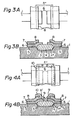
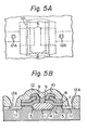
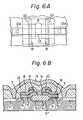
- Figs. lA through 6A and 1B through 6B are diagrams illustrating the manufacturing steps of one embodiment of the semiconductor memory device of the present invention, in which Figs. 1A through 6A are top plan views showing the main part of the device and Figs. 1B through 6B are cross--sectional views thereof.
- Boron ions (B + ) are injected in a silicon (Si) semiconductor substrate 1 in a dose of, for example, about 1 x 10 13 ions per cm 2 according to the ion implantation method to form a p + type channel cut region 2.
- Arsenic ions are injected in a dose of, for example, about 5 x 10 15 per cm 2 according to the ion implantation method to form an n + type region 3 for a line of a power source Vss of the ground potential level.
- a silicon dioxide (SiO 2 ) field insulating layer 4 having a thickness of, for example, about 5,000 to 0 about 10,000 A is formed, for example, according to the selective thermal oxidation method using a silicon nitride (Si 3 N 4 ) film mask. When the mask is removed, the surface of the active region of the substrate 1 is exposed.
- a first insulating layer 5 of silicon dioxide 0 having a thickness of about 700 to about 1,000 A is formed on the exposed surface of the active region of the substrate 1, for example, according to the thermal oxidation method.
- a polycrystalline silicon layer 6, forming the first gate electrode in an electrically floating state is formed in a thickness of about 4,000 to about 5,000 A, for example, according to the chemical vapor phase deposition method.
- a silicide of a refractory metal such as molybdenum silicide or tungsten silicide, may be used.
- the polycrystalline silicon layer 6 and the silicon dioxide insulating layer 5 are patterned according to the photolithographic technique.
- a second silicon dioxide insulating layer 7 having a thickness of about 800 to about 1,000 A is formed on the exposed surface of the active region of the substrate 1 and on the polycrystalline silicon layer 6, for example, according to the thermal oxidation method.
- a polycrystalline silicon layer 8, forming the second gate electrode (i.e., the control electrode), is 0 grown to a thickness of about 4,000 to about 5,000 A according to the chemical vapor phase deposition method.
- the second polycrystalline silicon layer 8 and the second insulating layer 7 are patterned according to the photolithographic technique.
- the portion of the second silicon dioxide layer 7 formed on the polycrystalline silicon layer 6 in the above-mentioned step (7), which portion has not been covered with the polycrystalline silicon layer 8 in the above-mentioned step (8), is removed whereby a portion of the polycrystalline silicon layer 6 is exposed.
- a third insulating layer 9 of silicon dioxide is grown to a thickness of, for example, about 50 to o about 300 A, for example, according to the thermal oxidation method on the exposed surface of the polycrystalline silicon layer 8, on the exposed surface of the polycrystalline silicon layer 6 and on the exposed surface of the substrate 1.
- the third insulating layer 9 of silicon dioxide should have a thickness sufficient for passage of electrons from the first polycrystalline silicon layer 6 (i.e., first gate electrode) to a third polycrystalline silicon layer 10 (i.e., an erasing electrode to be formed on the third insulating layer 9) through the tunneling effect thereby discharging the first gate electrode, when the written information is erased in the resulting memory device.
- This thickness of the third insulating layer 9 should preferably be maintained at least at a part of the side wall 6' of the first polycrystalline silicon layer 6.
- Such thickness for the intended passage of electrons by the tunnel effect is 0 usually in the range of from 50 to 300 A, more preferably from 100 to 200 A.
- a polycrystalline silicon layer 10 for the third gate electrode (i.e., the erasing electrode) is grown to a o thickness of about 4,000 A according to the chemical vapor phase deposition method.
- the polycrystalline silicon layer 10 and the third insulating layer 9 are patterned according to the photolithographic technique.
- Arsenic ions are injected according to the ion inplantation method or other appropriate technique to form an n + type region 11.
- An insulating layer 12 of phosphosilicate glass or silicon dioxide is formed in a thickness of, for example, about 1 micron according to the chemical vapor phase deposition method.
- the insulating layer 12 is patterned according to the photolithographic technique to form electrode contact windows 12A.
- An aluminum (Al) film having a thickness of, for example, about 1 micron is formed according to the vacuum evaporation deposition method, and the aluminum film is patterned according to the photolithographic technique to form a bit line electrode lead 13.
- a cover film, electrode windows and the like are formed according to customary techniques.
- a semiconductor memory device is obtained wherein, as illustrated in Figs. 6A and 6B, one or more pairs of the first gate electrodes 6 and one or more pairs of the control electrodes 8 are disposed so that the two first gate electrodes 6 in each pair are symmetric to each other, relative to the erasing electrode 10, and the two control electrodes 8 in each pair are also symmetric to each other, relative to the erasing electrode 10.
- the device which has been fabricated according to the above procedures is operated as follows.
- the polycrystalline silicon layer 10 for the third gate electrode which acts as a charge-releasing gate or an erasing electrode, and the n type region 3 acting, as a source region, are maintained at the same potential level (ground potential level), and in this state, a positive high voltage is applied to the polycrystalline silicon layer 8 for the second gate electrode which acts as a control gate, whereby electrons are injected into the polycrystalline silicon layer 6 for the first floating gate electrode.
- the voltage applied is usually in the range of from about 20 to about 30 volts, preferably from about 20 to about 25 volts.
- the polycrystalline silicon layer 10 for the third gate electrode which acts as a charge-releasing gate, is maintained at the ground potential level, and a voltage of, for example, +5 V is applied to the polycrystalline silicon layer 8 forming the second gate electrode and a voltage of, for example, +1 V is applied to the aluminum lead 13, which acts as a bit line to read the difference of the threshold voltage (Vth) among the respective memory cells.
- Vth threshold voltage
- the same high voltage is applied to both the polycrystalline silicon layer 8, forming the second gate electrode which acts as a control gate, and the polycrystalline silicon layer 10, forming the third gate electrode which acts as a charge-releasing gate, or a positive high voltage is applied only to the polycrystalline silicon layer 10 forming the third gate electrode, whereby charges accumulated in the polycrystalline silicon layer 6 for the first gate electrode are released.
- the voltage applied in this erasing stage may be approximately the same as that applied in the above-mentioned writing stage, that is, usually in the range of from about 20 to about 30 volts, preferably from about 20 to about 25 volts.
- This release of charges in the polycrystalline silicon layer 6 forming the first gate electrode and passing to the polycrystalline silicon layer 10, forming the third gate electrode, is accomplished by utilizing the tunnel effect generated, because the intervening insulating layer 9 is very thin, that is, 50 to 300 A.
- an improved EPROM device comprising (i) a first gate electrode in an electrically floating state, at least a part of which confronts a channel region of a semiconductor substrate and which is separated by a thin insulating layer from the channel region, (ii) a second gate electrode (i.e., a control electrode), at least a part of which confronts the first gate electrode and is separated by a thin insulating layer from the first gate electrode, and (iii) a third gate electrode (i.e., an erasing electrode), at least apart of which confronts the first gate electrode (and, preferably, also the second gate electrode) and which is separated by a very thin insulating layer.
- charges accumulated in the first gate electrode i.e., the floating gate
- a relatively low voltage i.e., about 20 to about 30 volts
Landscapes
- Engineering & Computer Science (AREA)
- Microelectronics & Electronic Packaging (AREA)
- Non-Volatile Memory (AREA)
- Semiconductor Memories (AREA)
Applications Claiming Priority (2)
| Application Number | Priority Date | Filing Date | Title |
|---|---|---|---|
| JP119213/80 | 1980-08-29 | ||
| JP55119213A JPS5743470A (en) | 1980-08-29 | 1980-08-29 | Semiconductor device |
Publications (2)
| Publication Number | Publication Date |
|---|---|
| EP0047153A1 true EP0047153A1 (fr) | 1982-03-10 |
| EP0047153B1 EP0047153B1 (fr) | 1985-02-06 |
Family
ID=14755735
Family Applications (1)
| Application Number | Title | Priority Date | Filing Date |
|---|---|---|---|
| EP81303949A Expired EP0047153B1 (fr) | 1980-08-29 | 1981-08-28 | Dispositif semi-conducteur à mémoire |
Country Status (4)
| Country | Link |
|---|---|
| US (1) | US4405995A (fr) |
| EP (1) | EP0047153B1 (fr) |
| JP (1) | JPS5743470A (fr) |
| DE (1) | DE3168790D1 (fr) |
Cited By (10)
| Publication number | Priority date | Publication date | Assignee | Title |
|---|---|---|---|---|
| EP0062460A3 (en) * | 1981-03-25 | 1983-02-09 | Fujitsu Limited | Electrically-erasable non-volatile semiconductor memory elements |
| EP0053878A3 (en) * | 1980-12-08 | 1983-07-20 | Tokyo Shibaura Denki Kabushiki Kaisha | Semiconductor memory device |
| US4861730A (en) * | 1988-01-25 | 1989-08-29 | Catalyst Semiconductor, Inc. | Process for making a high density split gate nonvolatile memory cell |
| EP0430426A3 (en) * | 1989-11-01 | 1991-06-12 | American Telephone And Telegraph Company | Semiconductor memory device |
| US5095344A (en) * | 1988-06-08 | 1992-03-10 | Eliyahou Harari | Highly compact eprom and flash eeprom devices |
| US5168465A (en) * | 1988-06-08 | 1992-12-01 | Eliyahou Harari | Highly compact EPROM and flash EEPROM devices |
| FR2693308A1 (fr) * | 1992-07-03 | 1994-01-07 | Commissariat Energie Atomique | Mémoire eeprom à triples grilles et son procédé de fabrication. |
| US5554553A (en) * | 1988-06-08 | 1996-09-10 | Harari; Eliyahou | Highly compact EPROM and flash EEPROM devices |
| US5677872A (en) * | 1995-05-31 | 1997-10-14 | Sandisk Corporation | Low voltage erase of a flash EEPROM system having a common erase electrode for two individual erasable sectors |
| DE19817127C2 (de) * | 1997-09-04 | 2001-07-12 | Mitsubishi Electric Corp | Nichtflüchtige Halbleiterspeichervorrichtungen mit schwebender Gateelektrode, Steuer- und Löschelektrode und zugehöriges Herstellungsverfahren |
Families Citing this family (14)
| Publication number | Priority date | Publication date | Assignee | Title |
|---|---|---|---|---|
| US4853895A (en) * | 1987-11-30 | 1989-08-01 | Texas Instruments Incorporated | EEPROM including programming electrode extending through the control gate electrode |
| US4924437A (en) * | 1987-12-09 | 1990-05-08 | Texas Instruments Incorporated | Erasable programmable memory including buried diffusion source/drain lines and erase lines |
| US5143860A (en) * | 1987-12-23 | 1992-09-01 | Texas Instruments Incorporated | High density EPROM fabricaiton method having sidewall floating gates |
| US4912676A (en) * | 1988-08-09 | 1990-03-27 | Texas Instruments, Incorporated | Erasable programmable memory |
| US4996668A (en) * | 1988-08-09 | 1991-02-26 | Texas Instruments Incorporated | Erasable programmable memory |
| JPH0287676A (ja) * | 1988-09-26 | 1990-03-28 | Ricoh Co Ltd | フローテイングゲート型不揮発性メモリ装置 |
| US5296396A (en) * | 1988-12-05 | 1994-03-22 | Sgs-Thomson Microelectronics S.R.L. | Matrix of EPROM memory cells with a tablecloth structure having an improved capacitative ratio and a process for its manufacture |
| IT1227989B (it) * | 1988-12-05 | 1991-05-20 | Sgs Thomson Microelectronics | Matrice di celle di memoria eprom con struttura a tovaglia con migliorato rapporto capacitivo e processo per la sua fabbricazione |
| JP2515009B2 (ja) * | 1989-01-13 | 1996-07-10 | 株式会社東芝 | 不揮発性半導体メモリの製造方法 |
| IT1229131B (it) * | 1989-03-09 | 1991-07-22 | Sgs Thomson Microelectronics | Matrice di memoria eprom con struttura a tovaglia e procedimento per la sua fabbricazione. |
| JPH085146B2 (ja) * | 1990-09-29 | 1996-01-24 | 福山ゴム工業株式会社 | ゴムクローラの製造方法 |
| KR970003845B1 (ko) * | 1993-10-28 | 1997-03-22 | 금성일렉트론 주식회사 | 이이피롬 프래쉬 메모리 셀, 메모리 디바이스 및 그 제조방법 |
| KR100217901B1 (ko) * | 1996-03-11 | 1999-09-01 | 김영환 | 플래쉬 이이피롬 셀 및 그 제조방법 |
| US9368775B2 (en) | 2004-02-06 | 2016-06-14 | Polyplus Battery Company | Protected lithium electrodes having porous ceramic separators, including an integrated structure of porous and dense Li ion conducting garnet solid electrolyte layers |
Citations (4)
| Publication number | Priority date | Publication date | Assignee | Title |
|---|---|---|---|---|
| US3825946A (en) * | 1971-01-15 | 1974-07-23 | Intel Corp | Electrically alterable floating gate device and method for altering same |
| US4099196A (en) * | 1977-06-29 | 1978-07-04 | Intel Corporation | Triple layer polysilicon cell |
| US4203158A (en) * | 1978-02-24 | 1980-05-13 | Intel Corporation | Electrically programmable and erasable MOS floating gate memory device employing tunneling and method of fabricating same |
| DE3002493A1 (de) * | 1979-01-24 | 1980-08-07 | Xicor Inc | Substratgekoppelte speicherzelle mit einem floating-gate und verfahren zum betrieb dieser zelle |
Family Cites Families (2)
| Publication number | Priority date | Publication date | Assignee | Title |
|---|---|---|---|---|
| JPS52106275A (en) * | 1976-03-03 | 1977-09-06 | Nec Corp | Floating type nonvoltile semiconductor memory element |
| US4161039A (en) * | 1976-12-15 | 1979-07-10 | Siemens Aktiengesellschaft | N-Channel storage FET |
-
1980
- 1980-08-29 JP JP55119213A patent/JPS5743470A/ja active Pending
-
1981
- 1981-08-24 US US06/295,617 patent/US4405995A/en not_active Expired - Lifetime
- 1981-08-28 EP EP81303949A patent/EP0047153B1/fr not_active Expired
- 1981-08-28 DE DE8181303949T patent/DE3168790D1/de not_active Expired
Patent Citations (6)
| Publication number | Priority date | Publication date | Assignee | Title |
|---|---|---|---|---|
| US3825946A (en) * | 1971-01-15 | 1974-07-23 | Intel Corp | Electrically alterable floating gate device and method for altering same |
| US4099196A (en) * | 1977-06-29 | 1978-07-04 | Intel Corporation | Triple layer polysilicon cell |
| US4203158A (en) * | 1978-02-24 | 1980-05-13 | Intel Corporation | Electrically programmable and erasable MOS floating gate memory device employing tunneling and method of fabricating same |
| US4203158B1 (fr) * | 1978-02-24 | 1992-09-22 | Intel Corp | |
| DE3002493A1 (de) * | 1979-01-24 | 1980-08-07 | Xicor Inc | Substratgekoppelte speicherzelle mit einem floating-gate und verfahren zum betrieb dieser zelle |
| US4274012A (en) * | 1979-01-24 | 1981-06-16 | Xicor, Inc. | Substrate coupled floating gate memory cell |
Non-Patent Citations (4)
| Title |
|---|
| Electronics, Vol. 52, No. 19, 13 September 1979 New York R.P. CAPECE et al. "Static RAM Tunnels for Nonvolatility" pages 39 to 40 * |
| IBM Technical Disclosure Bulletin, Vol. 17, No. 8, January 1975 New York S. DASGUPTA et al. "Dual-Gate Famos Memory Cell" page 2266 * |
| IBM Technical Disclosure Bulletin, Vol. 21, No. 8, January 1979 New York T.A. LARSEN et al. "Floating-Gate Device with Dual Control Gates" page 3368 * |
| IBM Technical Disclosure Bulletin, Vol. 22, No. 6, November 1979 New York C.R. HOFFMAN "Floating Gate Nonvolatile Memory Cell" pages 2403 to 2404 * |
Cited By (14)
| Publication number | Priority date | Publication date | Assignee | Title |
|---|---|---|---|---|
| EP0053878A3 (en) * | 1980-12-08 | 1983-07-20 | Tokyo Shibaura Denki Kabushiki Kaisha | Semiconductor memory device |
| EP0062460A3 (en) * | 1981-03-25 | 1983-02-09 | Fujitsu Limited | Electrically-erasable non-volatile semiconductor memory elements |
| US4503519A (en) * | 1981-03-25 | 1985-03-05 | Fujitsu Limited | Semiconductor non-volatile memory element of an electrically erasable type |
| US4861730A (en) * | 1988-01-25 | 1989-08-29 | Catalyst Semiconductor, Inc. | Process for making a high density split gate nonvolatile memory cell |
| US5168465A (en) * | 1988-06-08 | 1992-12-01 | Eliyahou Harari | Highly compact EPROM and flash EEPROM devices |
| US5095344A (en) * | 1988-06-08 | 1992-03-10 | Eliyahou Harari | Highly compact eprom and flash eeprom devices |
| US5554553A (en) * | 1988-06-08 | 1996-09-10 | Harari; Eliyahou | Highly compact EPROM and flash EEPROM devices |
| EP0430426A3 (en) * | 1989-11-01 | 1991-06-12 | American Telephone And Telegraph Company | Semiconductor memory device |
| FR2693308A1 (fr) * | 1992-07-03 | 1994-01-07 | Commissariat Energie Atomique | Mémoire eeprom à triples grilles et son procédé de fabrication. |
| WO1994001892A1 (fr) * | 1992-07-03 | 1994-01-20 | Commissariat A L'energie Atomique | Memoire eeprom de type flash a triples grilles et son procede de fabrication |
| US5679970A (en) * | 1992-07-03 | 1997-10-21 | Commissariat A L'energie Atomique | Triple gate flash-type EEPROM memory and its production process |
| US5677872A (en) * | 1995-05-31 | 1997-10-14 | Sandisk Corporation | Low voltage erase of a flash EEPROM system having a common erase electrode for two individual erasable sectors |
| DE19817127C2 (de) * | 1997-09-04 | 2001-07-12 | Mitsubishi Electric Corp | Nichtflüchtige Halbleiterspeichervorrichtungen mit schwebender Gateelektrode, Steuer- und Löschelektrode und zugehöriges Herstellungsverfahren |
| US6329688B1 (en) | 1997-09-04 | 2001-12-11 | Mitsubishi Denki Kabushiki Kaisha | Nonvolatile semiconductor memory device and method of manufacturing the same |
Also Published As
| Publication number | Publication date |
|---|---|
| US4405995A (en) | 1983-09-20 |
| DE3168790D1 (en) | 1985-03-21 |
| EP0047153B1 (fr) | 1985-02-06 |
| JPS5743470A (en) | 1982-03-11 |
Similar Documents
| Publication | Publication Date | Title |
|---|---|---|
| US4405995A (en) | Semiconductor memory drive | |
| US6760258B2 (en) | Means to erase a low voltage programmable and erasable flash EEPROM | |
| EP0182198B1 (fr) | Dispositif électriquement programmable à un seul transistor et procédé | |
| US4412311A (en) | Storage cell for nonvolatile electrically alterable memory | |
| US4881108A (en) | Semiconductor device | |
| US5585293A (en) | Fabrication process for a 1-transistor EEPROM memory device capable of low-voltage operation | |
| US4957877A (en) | Process for simultaneously fabricating EEPROM cell and flash EPROM cell | |
| US20080020527A1 (en) | Non-volatile memory cell having a silicon-oxide-nitride-oxide-silicon gate structure and fabrication method of such cell | |
| KR100385041B1 (ko) | Eeprom 메모리 셀 및 그 제조 방법 | |
| US20020041526A1 (en) | Nonvolatile semiconductor memory device, process of manufacturing the same and method of operating the same | |
| US6232634B1 (en) | Non-volatile memory cell and method for manufacturing same | |
| GB1575960A (en) | Electrically erasable non-volatile semiconductor memory | |
| EP0579779B1 (fr) | Dispositif de memoire remanente a semi-conducteurs, modifiable par commande electrique, a transistor unique | |
| US5999453A (en) | Nonvolatile semiconductor memory | |
| JPS649741B2 (fr) | ||
| US5883835A (en) | Control method for non-volatile memory | |
| WO1996027904A1 (fr) | Eeprom sur couche isolante | |
| US4467452A (en) | Nonvolatile semiconductor memory device and method of fabricating the same | |
| JPH05251669A (ja) | 半導体記憶装置およびその書き換え方法 | |
| JP2928973B2 (ja) | 3重ウェルcmos構造を有するフラッシュeeprom | |
| US7118967B1 (en) | Protection of charge trapping dielectric flash memory devices from UV-induced charging in BEOL processing | |
| JPS6178169A (ja) | 半導体記憶装置 | |
| JPH05206412A (ja) | 半導体メモリー装置およびその作製方法 | |
| EP0464196B1 (fr) | Dispositif a memoire a semi-conducteurs remanente electromodifiable a transistor unique et a porte flottante recristallisee | |
| JPS58112370A (ja) | 半導体不揮発性記憶装置 |
Legal Events
| Date | Code | Title | Description |
|---|---|---|---|
| PUAI | Public reference made under article 153(3) epc to a published international application that has entered the european phase |
Free format text: ORIGINAL CODE: 0009012 |
|
| AK | Designated contracting states |
Designated state(s): DE FR GB IT LU NL SE |
|
| RBV | Designated contracting states (corrected) |
Designated state(s): DE FR GB IT LI LU NL SE |
|
| 17P | Request for examination filed |
Effective date: 19820609 |
|
| GRAA | (expected) grant |
Free format text: ORIGINAL CODE: 0009210 |
|
| AK | Designated contracting states |
Designated state(s): DE FR GB NL |
|
| REF | Corresponds to: |
Ref document number: 3168790 Country of ref document: DE Date of ref document: 19850321 |
|
| ET | Fr: translation filed | ||
| PLBE | No opposition filed within time limit |
Free format text: ORIGINAL CODE: 0009261 |
|
| STAA | Information on the status of an ep patent application or granted ep patent |
Free format text: STATUS: NO OPPOSITION FILED WITHIN TIME LIMIT |
|
| 26N | No opposition filed | ||
| PGFP | Annual fee paid to national office [announced via postgrant information from national office to epo] |
Ref country code: GB Payment date: 19990825 Year of fee payment: 19 |
|
| PGFP | Annual fee paid to national office [announced via postgrant information from national office to epo] |
Ref country code: NL Payment date: 19990830 Year of fee payment: 19 |
|
| PGFP | Annual fee paid to national office [announced via postgrant information from national office to epo] |
Ref country code: FR Payment date: 20000811 Year of fee payment: 20 |
|
| PGFP | Annual fee paid to national office [announced via postgrant information from national office to epo] |
Ref country code: DE Payment date: 20000822 Year of fee payment: 20 |
|
| PG25 | Lapsed in a contracting state [announced via postgrant information from national office to epo] |
Ref country code: GB Free format text: LAPSE BECAUSE OF NON-PAYMENT OF DUE FEES Effective date: 20000828 |
|
| PG25 | Lapsed in a contracting state [announced via postgrant information from national office to epo] |
Ref country code: NL Free format text: LAPSE BECAUSE OF NON-PAYMENT OF DUE FEES Effective date: 20010301 |
|
| GBPC | Gb: european patent ceased through non-payment of renewal fee |
Effective date: 20000828 |
|
| NLV4 | Nl: lapsed or anulled due to non-payment of the annual fee |
Effective date: 20010301 |