EP0049997A2 - Für die Herstellung als integrierte Schaltung geeignete Filterschaltung - Google Patents
Für die Herstellung als integrierte Schaltung geeignete Filterschaltung Download PDFInfo
- Publication number
- EP0049997A2 EP0049997A2 EP81304633A EP81304633A EP0049997A2 EP 0049997 A2 EP0049997 A2 EP 0049997A2 EP 81304633 A EP81304633 A EP 81304633A EP 81304633 A EP81304633 A EP 81304633A EP 0049997 A2 EP0049997 A2 EP 0049997A2
- Authority
- EP
- European Patent Office
- Prior art keywords
- circuit
- time
- output
- input
- constant
- Prior art date
- Legal status (The legal status is an assumption and is not a legal conclusion. Google has not performed a legal analysis and makes no representation as to the accuracy of the status listed.)
- Granted
Links
Images


Classifications
-
- H—ELECTRICITY
- H03—ELECTRONIC CIRCUITRY
- H03H—IMPEDANCE NETWORKS, e.g. RESONANT CIRCUITS; RESONATORS
- H03H11/00—Networks using active elements
- H03H11/02—Multiple-port networks
- H03H11/04—Frequency selective two-port networks
Definitions
- the present invention relates to a time-constant circuit, and more particularly to a time-constant circuit which can form a filter circuit suitable for being fabricated into an integrated circuit.
- inductive elements L
- IC integrated circuit
- R resistors
- Fig. 1 is a schematic diagram illustrating an example of the 2nd order low pass filter (hereinafter referred to as LPF) formed in an active filter, where an impedance converter 3 has a sufficiently high input impedance and a sufficiently low output impedance with the voltage gain of unity.
- the transfer function H( ⁇ ) of the 2nd order LPF can be expressed as follows.
- the resonance frequency ⁇ o and the value Q which represents the quality of the circuit are expressed as follows.
- the resistance value ratio and the capacitance value ratio can be made substantially constant.
- the accuracy of each absolute value is not so good.
- the absolute value accuracy of the resistance is about ⁇ 15% and that of the capacitance is about ⁇ 12%
- the accuracy of the resistance value ratio and the capacitance value ratio can be made approximately ⁇ 1% and ⁇ 0.1%, respectively.
- the spread of the value of Q which is determined by the resistance value ratio and the capacitance value ratio can be made small without difficulty
- the accuracy of the resonance frequency which is determined by the absolute value of the resistance and capacitance, ranges approximately ⁇ 20%.
- the resonance frequency wo is a very important parameter for determining the cut-off frequency of the LPF, and it is hardly available for the practical use if the resonance frequency spreads in such a range as ⁇ 20%.
- a low-order filter such as in 2nd order may meet the requirement in this arrangement, however, filters in higher order are often demanded.
- a high order filter is made by combination of 2nd order filters, and the arrangement of the external resistors and capacitors not only causes an increase in the number of circuit components but necessitates much IC pins.
- the filter circuit is not suitable for being fabricated into an integrated circuit.
- a time-constant circuit is formed of a resistor, a capacitor, a variable gain amplifier which is controlled by a DC signal, and an impedance converter.
- Such time-constant circuits are combined to form an integrated filter circuit having a small number of peripheral components and pins, wherein the gain of each variable gain amplifier within 2nd order or higher order filters is adjusted together by a DC potential, thereby compensating the spread of the RC time-constant of the circuits within the integrated circuit.
- the spread of the resistance and capacitance values of the filter circuit integrated within the same integrated circuit can be compensated with the same DC control voltage, thereby permitting the integration of all resistors and capacitors for the time-constant circuits within the integrated circuit merely by providing a single control terminal, whereby the number of components can be reduced effectively, and the large scale integration is made possible due to a small number of terminals needed, thus the invention significantly contributes to the manufacture of compact filter circuits.
- Fig. 2 is a block diagram showing an example of the time-constant circuit which is the primary block of the present invention.
- the circuit includes a first input terminal 4 for the time-constant circuit, an output terminal 5, a second input terminal 6, an impedance converter 3 having a voltage gain of unity, a variable gain differential amplifier 7, the gain of which varies in the range from 0 to 1, an adder circuit 8, a capacitor 9, and a resistor 10.
- the capacitor 9 has the value of C 3 and the resistor 10 has the value of R 3 .
- the transfer function H 1 (w) seen from the input terminal 4 to the output terminal 5 with the input terminal 6 being grounded can be expressed as:
- the transfer function H 2 ( ⁇ ) seen from the input terminal 6 to the output terminal 5-with the input terminal 4 being grounded can be expressed as:
- circuit of Fig. 2 is equivalent to the time-constant circuit shown in Fig. 3, provided:
- the spread of the time constant created by a capacitor and a resistor fabricated within the integrated circuit is in the range of ⁇ 20%, thus it can be compensated by this circuit arrangement.
- Fig. 4 shows an embodiment of the present invention where two of the time-constant circuit shown in Fig. 2 are combined to constitute a 2nd order LPF, which includes an input terminal 11 for the 2nd order LPF, an output terminal 12 for the 2nd order LPF, a first time-constant circuit 13, and a second time-constant circuit 14.
- Variable gain differential amplifiers 7 and 7' in the time-constant circuits 13 and 14, respectively, have an identical gain of k.
- R 7 , C 7 , R 81 C 8 in Fig. 5 are in the following relation to the value R 5 of the resistor 10 and the value C 5 of the capacitor 9 in the first time-constant circuit 13 and the value R 6 of the resistor 10' and the value C 6 of the capacitor 9' in the second time-constant circuit 14:
- the transfer function H 3 ( ⁇ ) of the 2nd order LPF shown in Fig. 5 can be expressed in the following equation.
- the value of Q and the resonance frequency ⁇ o of the circuit of Fig. 4 can be expressed as follows.
- the value of Q is not varied by changing the gain k, and thus the resonance frequency ⁇ o of the circuit of Fig. 4 can be varied without affecting the value of Q. Consequently, the spread of the resonance frequency due to the spread of the absolute values of capacitors and resistors can be compensated by varying the gain - k of the variable gain differential amplifiers 7 and 7'. Moreover, the two variable gain differential amplifiers 7 and 7' have exactly the same gain, allowing the control with a common DC voltage.
- LPFs of much higher order can be realized by combination of the above 2nd order LPFs.
- the absolute values of resistors and capacitors of 2nd order LPFs have the same trend of spreading. That is, they spread identically from the desired time constant and this allows all the variable gain differential amplifiers to have the same gain, which can be controlled with a single DC voltage.
- a plurality of filters fabricated within an integrated circuit have the same spread of time constant from the desired time constant, thereby allowing their adjustment for the desired time constant with a single DC voltage.
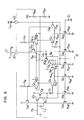
- Fig. 6 shows an example of the practical circuit for the embodiment shown in Fig. 4.
- resistor R 5 and capacitor C 5 correspond to the resistor 10 and the capacitor 9 of the first time-constant circuit 13 shown in Fig. 4
- resistor R 6 and capacitor C 6 correspond to the resistor 10' and the capacitor 9' of the second time-constant circuit 14 shown in Fig. 4.
- Darlington-coupled transistors Q 1 and Q 2 constitute the impedance converter 3 in the first time-constant circuit 13 shown in Fig. 4
- differential transistor pairs Q 3 and Q 4 , and Q 7 and Q 8 constitute the variable gain differential amplifier 7 in the first time-constant circuit 13.
- Transistors Q 5 and Q 6 constitute the impedance converter 3' in the second time-constant circuit 14, and differential transistor pairs Q 9 and Q 10 , and Q 11 and Q 12 constitute the variable gain differential amplifier 7' in the second time-constant circuit 14.
- Reference numbers 20 and 22 denote pins on the integrated circuit, 21 is an external variable resistor for controlling the gain of the variable gain amplifier, C 9 is an external signal smoothing capacitor, and Q 15 to Q 20 are transistors for the constant current sources.
- variable gain differential amplifiers 7 and 7' are achieved by the differential pairs Q 7 and Q 8 , and Q 9 and Q 10 in a current switching mode.
- the transistors Q 11 and Q 12 constituting the variable gain differential amplifier 7' in the second time-constant circuit 14 are adapted to serve also for a part of an adder circuit 8 in the first time-constant circuit 13 so that the collector current of the transistor Q 12 is added to the collector current of the transistor Q 7 .
- the adder circuit 8' simply buffers the output of the variable gain differential amplifier 7'. Also to make the circuit simple, the adder circuit 8' is omitted from the circuit of Fig. 6, and the collector current of the transistor Q 9 is converted into a voltage through a resistor R 17 and outputted through a low impedance buffer transistor Q 13 . Although some circuit components are shared or omitted for simplifying the circuit, it does not means the alteration of the concept, but it is easily possible to consider the circuit in the original arrangement.
- resistors R 12 ' R13' R14' R 17' R 20 , R21' R 26 , and R 29 should be set, for example, to meet the following conditions.
- Re is the emitter operating resistance of the transistors Q 3 , Q 4 , Q 11 and Q 12 ,
- Fig. 7 shows an embodiment of the present invention for constructing a 2nd order high-pass filter (HPF) circuit.
- the transfer function H 4 ( ⁇ ), the value of Q and the resonance frequency ⁇ o of the HPF circuit of Fig. 7 are expressed as follows.
- reference number 15 denotes an input terminal and 16 is an output terminal.
- Fig. 8 shows an embodiment of the present invention for constructing a 2nd order band-pass filter (BPF).
- the transfer function H 5 ( ⁇ ), the value of Q and the resonance frequency wo of the BPF circuit of Fig. 8 are expressed as follows.
- reference number 17 denotes an input terminal
- 18 is an output terminal
- 19 is an amplifier
- 20 is an input terminal.
- the 2nd order BPF needs an additional amplifier having a gain of two and a resistor, it can be constructed basically by combination of two time-constant circuits.
- any higher order filter can be composed by combination of a 2nd order LPF, 2nd order HPF, 2nd order BPF, 1st order LPF and a 1st order HPF.
- the present invention easily provides a filter having desired characteristics by combining a 2nd order LPF, HPF and BPF, and a 1st order LPF and BPF as described in the foregoing embodiments.
Landscapes
- Networks Using Active Elements (AREA)
Priority Applications (1)
| Application Number | Priority Date | Filing Date | Title |
|---|---|---|---|
| AT81304633T ATE11618T1 (de) | 1980-10-07 | 1981-10-06 | Fuer die herstellung als integrierte schaltung geeignete filterschaltung. |
Applications Claiming Priority (2)
| Application Number | Priority Date | Filing Date | Title |
|---|---|---|---|
| JP55139400A JPS5763922A (en) | 1980-10-07 | 1980-10-07 | Integrated filter circuit |
| JP139400/80 | 1980-10-07 |
Publications (3)
| Publication Number | Publication Date |
|---|---|
| EP0049997A2 true EP0049997A2 (de) | 1982-04-21 |
| EP0049997A3 EP0049997A3 (en) | 1982-10-20 |
| EP0049997B1 EP0049997B1 (de) | 1985-01-30 |
Family
ID=15244386
Family Applications (1)
| Application Number | Title | Priority Date | Filing Date |
|---|---|---|---|
| EP81304633A Expired EP0049997B1 (de) | 1980-10-07 | 1981-10-06 | Für die Herstellung als integrierte Schaltung geeignete Filterschaltung |
Country Status (5)
| Country | Link |
|---|---|
| US (1) | US4456885A (de) |
| EP (1) | EP0049997B1 (de) |
| JP (1) | JPS5763922A (de) |
| AT (1) | ATE11618T1 (de) |
| DE (1) | DE3168657D1 (de) |
Cited By (1)
| Publication number | Priority date | Publication date | Assignee | Title |
|---|---|---|---|---|
| GB2353420A (en) * | 1999-08-19 | 2001-02-21 | Fast Analog Solutions Ltd | An integrated RC bandpass filter with automatic centre frequency calibration |
Families Citing this family (4)
| Publication number | Priority date | Publication date | Assignee | Title |
|---|---|---|---|---|
| JPS61224510A (ja) * | 1985-03-28 | 1986-10-06 | Matsushita Electric Ind Co Ltd | 周波数選択回路 |
| US4671316A (en) * | 1985-05-20 | 1987-06-09 | Botnick Irlin H | Faucet manifold |
| DE4004135A1 (de) * | 1990-02-10 | 1991-08-14 | Thomson Brandt Gmbh | Frequenzgangkompensierte schaltung |
| JP4647361B2 (ja) * | 2005-03-29 | 2011-03-09 | ルネサスエレクトロニクス株式会社 | 半導体集積回路 |
Family Cites Families (2)
| Publication number | Priority date | Publication date | Assignee | Title |
|---|---|---|---|---|
| US3786363A (en) * | 1973-01-05 | 1974-01-15 | Us Navy | Voltage-controlled low-pass filter |
| JPS5226145A (en) * | 1975-08-25 | 1977-02-26 | Tamura Electric Works Ltd | Automatic gain adjustment circuit |
-
1980
- 1980-10-07 JP JP55139400A patent/JPS5763922A/ja active Pending
-
1981
- 1981-10-05 US US06/308,589 patent/US4456885A/en not_active Expired - Fee Related
- 1981-10-06 AT AT81304633T patent/ATE11618T1/de not_active IP Right Cessation
- 1981-10-06 DE DE8181304633T patent/DE3168657D1/de not_active Expired
- 1981-10-06 EP EP81304633A patent/EP0049997B1/de not_active Expired
Cited By (3)
| Publication number | Priority date | Publication date | Assignee | Title |
|---|---|---|---|---|
| GB2353420A (en) * | 1999-08-19 | 2001-02-21 | Fast Analog Solutions Ltd | An integrated RC bandpass filter with automatic centre frequency calibration |
| US6340913B1 (en) | 1999-08-19 | 2002-01-22 | Fast Analog Solutions Limited | Filter circuit with positive feedback loop |
| GB2353420B (en) * | 1999-08-19 | 2003-10-29 | Fast Analog Solutions Ltd | Filter circuit |
Also Published As
| Publication number | Publication date |
|---|---|
| EP0049997A3 (en) | 1982-10-20 |
| ATE11618T1 (de) | 1985-02-15 |
| US4456885A (en) | 1984-06-26 |
| JPS5763922A (en) | 1982-04-17 |
| DE3168657D1 (en) | 1985-03-14 |
| EP0049997B1 (de) | 1985-01-30 |
Similar Documents
| Publication | Publication Date | Title |
|---|---|---|
| JP3316038B2 (ja) | 演算トランスコンダクタンス増幅器・キャパシタ対用の周波数同調システム | |
| EP0435472B1 (de) | Aktives Filter | |
| WO1981002819A1 (en) | Analog integrated filter circuit | |
| EP0052117B1 (de) | Biquadratisches aktives filter im strom-modus | |
| EP0049997A2 (de) | Für die Herstellung als integrierte Schaltung geeignete Filterschaltung | |
| GB2224406A (en) | Filter circuit arrangement | |
| EP0696104B1 (de) | Aktives Bandpassfilter | |
| US5574398A (en) | Active bandpass filter | |
| JPH0648775B2 (ja) | リープフロッグ・フィルタ | |
| JPH04148388A (ja) | 時定数可変形の微分器 | |
| JPS6362133B2 (de) | ||
| JPH06104666A (ja) | 可変電圧電流変換回路 | |
| US5293086A (en) | Polar leapfrog filter | |
| JPS63193710A (ja) | 積分回路 | |
| JPS61170113A (ja) | 2次アクテイブ位相等価器 | |
| JP3308352B2 (ja) | 可変遅延回路 | |
| JP2590877B2 (ja) | グラフィックイコライザ回路 | |
| EP0665646A1 (de) | Filterschaltung | |
| JPH0648774B2 (ja) | 積分回路 | |
| JPH08256040A (ja) | 容量装置およびそれを用いたフィルタ装置 | |
| KR940009396B1 (ko) | 저역 통과 필터 | |
| JP3148458B2 (ja) | アクティブフィルタ | |
| JPH0114726B2 (de) | ||
| JP3301989B2 (ja) | アクティブフィルタ回路 | |
| JPH04150513A (ja) | フィルタ回路 |
Legal Events
| Date | Code | Title | Description |
|---|---|---|---|
| PUAI | Public reference made under article 153(3) epc to a published international application that has entered the european phase |
Free format text: ORIGINAL CODE: 0009012 |
|
| AK | Designated contracting states |
Designated state(s): AT DE FR GB IT |
|
| PUAL | Search report despatched |
Free format text: ORIGINAL CODE: 0009013 |
|
| AK | Designated contracting states |
Designated state(s): AT DE FR GB IT |
|
| 17P | Request for examination filed |
Effective date: 19830111 |
|
| ITF | It: translation for a ep patent filed | ||
| GRAA | (expected) grant |
Free format text: ORIGINAL CODE: 0009210 |
|
| AK | Designated contracting states |
Designated state(s): AT DE FR GB IT |
|
| REF | Corresponds to: |
Ref document number: 11618 Country of ref document: AT Date of ref document: 19850215 Kind code of ref document: T |
|
| REF | Corresponds to: |
Ref document number: 3168657 Country of ref document: DE Date of ref document: 19850314 |
|
| ET | Fr: translation filed | ||
| PLBE | No opposition filed within time limit |
Free format text: ORIGINAL CODE: 0009261 |
|
| STAA | Information on the status of an ep patent application or granted ep patent |
Free format text: STATUS: NO OPPOSITION FILED WITHIN TIME LIMIT |
|
| 26N | No opposition filed | ||
| GBPC | Gb: european patent ceased through non-payment of renewal fee | ||
| PG25 | Lapsed in a contracting state [announced via postgrant information from national office to epo] |
Ref country code: FR Free format text: LAPSE BECAUSE OF NON-PAYMENT OF DUE FEES Effective date: 19880630 |
|
| PG25 | Lapsed in a contracting state [announced via postgrant information from national office to epo] |
Ref country code: DE Effective date: 19880701 |
|
| REG | Reference to a national code |
Ref country code: FR Ref legal event code: ST |
|
| PG25 | Lapsed in a contracting state [announced via postgrant information from national office to epo] |
Ref country code: GB Effective date: 19881118 |
|
| PGFP | Annual fee paid to national office [announced via postgrant information from national office to epo] |
Ref country code: AT Payment date: 19900926 Year of fee payment: 10 |
|
| ITTA | It: last paid annual fee | ||
| PG25 | Lapsed in a contracting state [announced via postgrant information from national office to epo] |
Ref country code: AT Effective date: 19911006 |