EP0050008A2 - Halbleiteranlage - Google Patents
Halbleiteranlage Download PDFInfo
- Publication number
- EP0050008A2 EP0050008A2 EP81304673A EP81304673A EP0050008A2 EP 0050008 A2 EP0050008 A2 EP 0050008A2 EP 81304673 A EP81304673 A EP 81304673A EP 81304673 A EP81304673 A EP 81304673A EP 0050008 A2 EP0050008 A2 EP 0050008A2
- Authority
- EP
- European Patent Office
- Prior art keywords
- potential
- transistor
- reference potential
- signal
- base
- Prior art date
- Legal status (The legal status is an assumption and is not a legal conclusion. Google has not performed a legal analysis and makes no representation as to the accuracy of the status listed.)
- Ceased
Links
Images


Classifications
-
- G—PHYSICS
- G11—INFORMATION STORAGE
- G11C—STATIC STORES
- G11C29/00—Checking stores for correct operation ; Subsequent repair; Testing stores during standby or offline operation
- G11C29/04—Detection or location of defective memory elements, e.g. cell constructio details, timing of test signals
- G11C29/50—Marginal testing, e.g. race, voltage or current testing
Definitions
- This invention relates to a semiconductor device, such as a bipolar semiconductor memory device.
- a semiconductor device comprises an internal circuit for generating at least one internal signal; means to generate a reference signal; means, connected to the internal circuit and to the reference potential generating means, to sense the difference in potential between the internal signal and the reference signal; and means to change the difference in potential between the internal signal and the reference signal in accordance with a normal mode and a test mode.
- a semiconductor device comprises a plurality of word lines; a plurality of hold lines; a plurality of pairs of bit lines; a plurality of word drivers each connected to a respective one of the word lines; a plurality of memory cells, each comprising two multi-emitter transistors having bases and collectors cross-coupled to form a bistable circuit and having one emitter of each such multi-emitter transistor connected to one of the bit lines and the other emitter of each such multi-emitter transistor connected to one of the hold lines, and comprising two loads connected to the multi-emitter transistors and to one of the word lines; a plurality of pairs of sensing transistors having emitters connected to one of the pairs of bit lines; means connected to the bases of the sensing transistors to generate a read reference potential for each base of the sensing transistors; and means to change the difference in potential between an internal signal and the read reference potential in accordance with a normal mode and a test mode.
- the bipolar semiconductor memory device comprises memory cells C 00,... , C 0,m-1,... , C n-1,0,... , C n-1,m-1 in n rows by m columns.
- Each memory cell is connected to one of the word lines W 0,... , W n-1 , to one of the hold lines H 0,... , H n-1 and to one of the pairs of bit lines B 0 , B 0 ; ...; B m-1 ,B m-1 .
- the word lines W 0,... , W n-1 are connected to word drivers T x0,... , T x,n-1 , respectively, while the hold lines H 0,...
- H n-1 are connected to constant current sources I H0,... , I H,n-1 , respectively.
- pairs of sensing transistors T S0 T S0 '; ...; T S,m-1 , T S, ' m-1 are connected to the pairs of bit lines B 0 , B 0 ; ...; B m-1 , B m-1 , respectively, which are connected through bit line drivers BD 0 ,... , BD m-1 , respectively, to data bit lines DB and DB which are also connected to constant current sources I R0 and I R1 , respectively.
- a sense amplifier SA which is activated by a chip selection circuit CS 1 , detects the data stored in the memory cells C 00,... , C n-1,m-1 and generates a data signal D OUT .
- the chip selection circuit CS 1 receives the inverted signal CS of a chip selection signal.
- a write amplifier WA receives a data input signal D IN and the inverted signal WE of a write enable signal.
- the write amplifier WA generates two output signals having the same read reference potential V R , regardless of the data input signal D IN . Contrary to this, during the write mode when the potential of the signal WE is low, the write amplifier WA generates two output signals having different potentials V D0 and V D1 in response to the potential of the data input signal D IN .
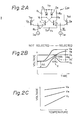
- Fig. 2A is a circuit diagram of the memory cell C 00 of Fig. 1.
- the cell C 00 is of a flip-flop type which comprises two multi-emitter transistors T 1 and T 2 with bases and collectors cross-coupled to form a bistable circuit.
- Each of the transistors T 1 and T 2 has one emitter connected to one emitter of the other, while the other emitter is connected to the bit line B 0 or B 0 .
- R 1 and R 2 are resistors
- D 1 and D 2 are diodes (for example, Schottky barrier diodes) for clamping the collector potentials of the transistors T 1 and T 2 . Therefore, the transistors T 1 and T 2 do not enter into the saturation state.
- Vw and V H are potentials of the word line W 0 and the hold line H 0 , respectively
- V C and V B are potentials of the collector and the base of the transistor T 1 .
- the resistors R 1 and R 2 are so large as to reduce the hold current I H in the non-selected state; however, in this case, in the selected state, the read current I R is so small that it takes a long time to charge the bit lines B 0 and B 0 .
- the diodes D I and D 2 are arranged parallel to the resistors R 1 and R 2 , respectively.
- This forward voltage is 0.7 to 0.8 V in a state wherein a sufficient current flows through the diode D 1 , while the forward voltage is smaller than 0.7 to 0.8 V in a state wherein a small current flows through the diode D 1 .
- V B > V R should be satisfied in order for the read current I R to flow through the emitter of the transistor T 1 to the bit line B 0 .
- V B V R
- the read current I R equals I R0 /2
- V B > V R or V B ⁇ V R the read current I R equals I R0 or zero. Therefore, when V B ⁇ V R (not selected), no current I R flows and accordingly, the collector potential V C is pulled up by the resistor R 1 and the diode D 1 . That is, the collector potential V c follows the word line potential V W , as illustrated in Fig. 2B.
- the collector potential V C As the collector potential V C is increased, the collector of the transistor T 1 and the base of the transistor T 2 are charged. In this case, due to the large resistance of the resistor R 1 , the charging current which is a collector current of the transistor T 1 is so large that the diode D 1 is turned on. As a result, the collector potential V C is rapidly increased, as indicated by the arrow X in Fig. 2B. Accordingly, as the base potential V B approaches the read reference potential V R , the read current I R begins to flow, so that the collector potential V C is again pulled down to a level which is determined by the diode D 1 in the selected state. Thus, the collector potential V C rises once and, after that, falls.
- the collector of the transistor T 2 and the base of the transistor T 1 are also charged by the current flowing through the resistor R 2 ; however, in this case, since the base potential V B is high in the non-selected state, the current flowing through the resistor R 2 which is a base current of the transistor T 1 , is not so large as to turn on the diode D 2 . Therefore, the base potential V B rises slowly and, in addition, since the transistor T 2 is turned off, the potential V B rises linearly.
- the collector potential V C has a peak characteristic and, accordingly, there is a problem in that the maximum of the collector potential V C approaches the read reference potential V R . That is, the collector potential may rise as indicated by a dotted line V C ', due to the fluctuation characteristics of the diodes D 1 and D 2 , and this causes a rise in the temperature of the chip or the like.
- the collector potential may rise as indicated by a dotted line V C ', due to the fluctuation characteristics of the diodes D 1 and D 2 , and this causes a rise in the temperature of the chip or the like.
- the value (V R - V C ) is called a noise margin.
- NM 0 is a noise margin at room temperature
- NM 1 is a noise margin at a high temperature.
- the value V R is set at an intermediate level between the base potential V B and the collector potential V C ; however, as the temperature rises, the difference between the potentials V B and V C becomes smaller, so that the noise margin also becomes smaller.
- Fig. 2B note that it may be desirable that the potential V R is shifted toward the word line potential V W , in order to increase the noise margin; however, in this case, the-difference between the potentials V R and V B becomes small, so that it is difficult to obtain read outputs at the bit lines B 0 and B 0 .
- the potential V R is set at an intermediate level between the potentials V B and V c in the selected state, as mentioned above.
- V C > V R is satisfied when the state is changed from non-selected to selected under an adverse condition, such as a high temperature condition.
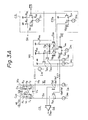
- Fig. 3A is a circuit diagram illustrating a first embodiment of the bipolar semiconductor memory device according to the present invention.
- the elements which are the same as those of Figs. 1 and 2A are denoted by the same references.
- a circuit CS 2 for decreasing the read reference potential V R in the test mone is added between the chip selection circuit CS 1 and the write amplifier WA.
- the chip selection circuit CS 1 comprises resistors R C1 and R C2 , a transistor T C1 having a base to which a reference potential V R1 ( ⁇ -1.3 V) is applied, a transistor T C2 having a base to which the inverted signal CS of a chip selection signal is supplied, and a constant current source I C1 .
- the transistors T C1 and T C2 form a current switch with regard to.the constant current source I C1 .
- the chip selection circuit CS 1 controls the sense amplifier SA. That is, when the potential of the signal CS is lower than the reference potential V R1 , the transistors T C1 and T C2 are turned on and off, respectively, so that the low potential of the collector of the transistor T C1 activates the sense amplifier SA.
- the write amplifier WA comprises transistors T W1 through T W5 , resistors R W1 and R W2 , diodes D 11 and D 12 , constant current sources I W1 , I W2 and I W3 .
- the transistors T W1 and T W2 form a current source with regard to the constant current source I W1
- the transistors T W3 and T W4 form a current switch with regard to the constant current source I W1 .
- the base potentials V DO and V D1 of the sensing transistors T S0 and T S0 ' are the same as the read reference potential V R by the emitter-follower transistors T W5 and T W6 .
- the transistor T W3 is turned on and in addition, one of the transistors T W1 and T W2 is turned on in response to the data input signal D IN .
- the transistor T W1 is turned on, while, if the potential of the signal D IN is higher than the reference potential V R1 , the transistor T W2 is turned on. Therefore, the base potentials V D0 and V D1 of the transistors T S0 and T S0 ' are different from each other.
- the reference potential V R2 is, for example, -2.1 V.
- the circuit CS 2 for decreasing the read potential V R in the test mode, comprises two transistors T C3 and T C4 and a current source IC2.
- the transistors T C3 and T C4 form a current switch with regard to the constant current source IC2.
- the base of transistor T C4 is connected commonly to the base of the transistor T C2 of the chip selection circuit CS 1 and, accordingly, the base of the transistor T C4 receives the chip selection signal CS.
- the collector of the transistor T C3 is connected commonly to the collector of the transistor T W4 of the write amplifier WA.
- a reference potential V R3 which is applied to the base of the transistor T C3 , is much lower than the other reference potentials V R1 and V R2 .
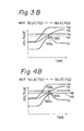
- the chip selection signal CS has a usual level, the potential of the signal CS is never lower than the reference potential V R3 , so that the transistor T C3 is always cut off. That is, during the usual mode, the presence of the circuit CS 2 has no effect. Therefore, a read reference potential V R having a sufficient noise margin NM 0 with regard to the collector potential V , as illustrated in Fig. 3B, is applied to the bases of the transistors T S0 and T S0 '.
- the potential of the signal CS is caused to be much lower than the usual high and low levels (non-selected and selected levels), so as to satisfy that the potential of the signal CS is lower than the reference potential V R3 .
- the transistor T C3 is turned on, so that an equivalent current flows through each of the resistors R W1 and R W2 and each of the diodes D 11 and D 12 .
- the equivalent currents flow into the constant current source I C2 .
- the read reference potential V R ' that is, each of the base potentials of the sensing transistors T S0 and T S0 ', is lower than the read reference potential V R during the usual mode, as illustrated in Fig. 3B.
- the potential of the signal WE is high, so that the currents I C2 and I W1 flow through the resistors R W1 and R W2 .
- the read reference potential V R ' during the test mode is lower than the read reference potential V R during the usual mode, without necessitating the condition I C2 > I W1 . Therefore, when the read operation is carried out by the read reference potential V R ', the noise margin with regard to the collector potential V C is indicated by NM 1 in Fig. 3B.
- This noise margin NM 1 corresponds to a high temperature state. Therefore, without forcing the chip to be in a high temperature state, checking or testing of the device at a high temperature state can be carried out at room temperature.
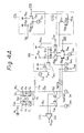
- Fig. 4A is a circuit diagram illustrating a second embodiment of the bipolar semiconductor memory device according to the present invention.
- the elements which are the same as those of Fig. 3A are denoted by the same references.
- the circuit CS 2 ' for decreasing the read potential V R in the test mode comprises a resistor R C3 instead of the transistor T C4 and the constant current source I C3 of Fig. 3A.
- the read reference potential V R ' corresponding to a high temperature state can not be arbitrarily changed, even if the potential of the signal CS is changed. Contrary to this, in Fig.
- the read reference potential corresponding to a high temperature state can be arbitrarily changed by changing the potential of the signal CS. That is, in F ig. 4B, the read reference potential V R1 ' and V R2 ' correspond to a first high temperature state and a second high temperature state, respectively. In this case, the first high temperature is lower than the second high temperature.
- the reference potential V R3 is determined so as to cut off the transistor T C3 when the potential of the signal CS is of a usual level, which is different from a test level.
- the potential of the signal CS is caused to be lower than a value (V R3 - V BE ) where V BE is the potential between the base and the emitter of the transistor T C3 , so as to cause the collector current I C3 to flow through the transistor T C3 .
- This current I C3 is represented by where V CS is the potential of the signal CS and V BE is a base-emitter voltage of the transistor T C3 ; then the current I C3 is changed by changing the potential V CS , which also changes the voltage drops in the resistors R W1 and R W2 .
- the read reference potential V R can be arbitrarily changed, as illustrated in Fig. 4B.
- checking or testing of the device of Fig. 4A at various high temperature states can be carried out at room temperature.
- Fig. 5 is a circuit diagram illustrating a third embodiment of the bipolar semiconductor memory device according to the present invention.
- the elements which are the same as those of Fig. 4A are denoted by the same references.
- the base of the transistor T C4 of the circuit CS 2 " is connected to a programmable element or a diode D P and to an external terminal TM, not to the chip selection circuit CS 1 . That is, during the test mode, the terminals of the diode D P are opened so that the potential of the base of the transistor T C4 is lower than the reference potential V R3 . As a result, the transistor T C3 remains conductive. After testing, that is, during the usual mode, the terminals of the diode D P are shorted so that the transistor T C4 is turned off.
- the operation of the circuit of Fig. 5 is similar to that of the circuit of Fig. 3A.
- Fig. 6A is a circuit diagram illustrating a fourth embodiment of the bipolar semiconductor memory device according to the present invention.
- the elements which are the same as those of Fig. 3A are denoted by the same references.
- a circuit CS 2 "' for increasing the potential of the word line W 0 which is similar to the circuit CS of Fig. 3A, is provided.
- the circuit CS 2 "' also comprises two transistors T C3 and T C4 and a constant current source I C2 .
- a reference potential V R3 is applied to the base of the transistor T C3 ' while the chip selection signal CS is supplied to the base of the transistor T C4 .
- a resistor R X1 is connected to a resistor R X2 of the word driver T X0 .
- the transistor T C4 is turned on, so that the base potential of the word driver T X0 is low as compared with the ground level. Contrary to this, during the test mode when the potential CS is lower than the reference potential V R3 ' the transistor T C4 is cut off, so that the base potential of the word driver T X0 rises toward the ground level. As a result, as illustrated in Fig. 6A, the word line potential V w ' , the base potential V B ' and the collector potential V C ' during the test mode are higher than the word line potential V W , the base potential V B and the collector potential V C during the usual mode, respectively.
- the read reference potential V R is not changed regardless of the usual and test modes, since the read reference potential V R is determined by the write amplifier WA . Therefore, the noise margin NM 1 during the test mode is smaller than the noise margin NM 0 during the usual mode. Note that this small noise margin NM 1 corresponds to a high temperature state. Thus, checking or testing of the device of Fig. 6A at a high temperature state can be carried out at room temperature.
- MOS broadly, MIS
- bipolar semiconductor device can be applied to a MOS (broadly, MIS) semiconductor device as well as the bipolar semiconductor device.
- the semiconductor device according to the present invention has an advantage in that checking or testing of the device for a high temperature state can be carried out at room temperature, since the noise margin is decreased by decreasing the read reference potential or by increasing the word line potential. Therefore, the manufacturing cost for the semiconductor device is reduced.
Landscapes
- Static Random-Access Memory (AREA)
- For Increasing The Reliability Of Semiconductor Memories (AREA)
- Techniques For Improving Reliability Of Storages (AREA)
- Dram (AREA)
Applications Claiming Priority (2)
| Application Number | Priority Date | Filing Date | Title |
|---|---|---|---|
| JP141656/80 | 1980-10-09 | ||
| JP55141656A JPS6010400B2 (ja) | 1980-10-09 | 1980-10-09 | 半導体集積回路装置 |
Publications (2)
| Publication Number | Publication Date |
|---|---|
| EP0050008A2 true EP0050008A2 (de) | 1982-04-21 |
| EP0050008A3 EP0050008A3 (de) | 1984-01-11 |
Family
ID=15297111
Family Applications (1)
| Application Number | Title | Priority Date | Filing Date |
|---|---|---|---|
| EP81304673A Ceased EP0050008A3 (de) | 1980-10-09 | 1981-10-08 | Halbleiteranlage |
Country Status (3)
| Country | Link |
|---|---|
| US (1) | US4459686A (de) |
| EP (1) | EP0050008A3 (de) |
| JP (1) | JPS6010400B2 (de) |
Families Citing this family (14)
| Publication number | Priority date | Publication date | Assignee | Title |
|---|---|---|---|---|
| DE3227121A1 (de) * | 1982-07-20 | 1984-01-26 | Siemens AG, 1000 Berlin und 8000 München | Schaltungsanordnung zum lesen bipolarer speicherzellen |
| US4742488A (en) * | 1982-10-25 | 1988-05-03 | Advanced Micro Devices, Inc. | Sense amplifier/write circuit for semiconductor memories |
| JPS59151386A (ja) * | 1983-01-31 | 1984-08-29 | Fujitsu Ltd | 半導体記憶装置 |
| US4719418A (en) * | 1985-02-19 | 1988-01-12 | International Business Machines Corporation | Defect leakage screen system |
| US4685086A (en) * | 1985-11-14 | 1987-08-04 | Thomson Components-Mostek Corp. | Memory cell leakage detection circuit |
| US4658380A (en) * | 1986-02-28 | 1987-04-14 | Ncr Corporation | CMOS memory margining control circuit for a nonvolatile memory |
| US4779043A (en) * | 1987-08-26 | 1988-10-18 | Hewlett-Packard Company | Reversed IC test device and method |
| US5200924A (en) * | 1989-03-30 | 1993-04-06 | Synergy Semiconductor Corporation | Bit line discharge and sense circuit |
| JPH0612896A (ja) * | 1992-04-28 | 1994-01-21 | Nec Corp | 半導体記憶装置 |
| KR0132756B1 (ko) * | 1993-03-15 | 1998-04-16 | 원본미기재 | 이씨엘(ecl) 회로의 번인 방법 및 장치 |
| US6694465B1 (en) * | 1994-12-16 | 2004-02-17 | Texas Instruments Incorporated | Low overhead input and output boundary scan cells |
| JP3866444B2 (ja) * | 1998-04-22 | 2007-01-10 | 東芝マイクロエレクトロニクス株式会社 | 半導体装置及びその内部信号モニタ方法 |
| US7016249B2 (en) * | 2003-06-30 | 2006-03-21 | Intel Corporation | Reference voltage generator |
| US7450416B1 (en) * | 2004-12-23 | 2008-11-11 | Spansion Llc | Utilization of memory-diode which may have each of a plurality of different memory states |
Family Cites Families (3)
| Publication number | Priority date | Publication date | Assignee | Title |
|---|---|---|---|---|
| JPS5375828A (en) * | 1976-12-17 | 1978-07-05 | Hitachi Ltd | Semiconductor circuit |
| JPS5833634B2 (ja) * | 1979-02-28 | 1983-07-21 | 富士通株式会社 | メモリセルアレイの駆動方式 |
| JPS5847792B2 (ja) * | 1979-07-26 | 1983-10-25 | 富士通株式会社 | ビット線制御回路 |
-
1980
- 1980-10-09 JP JP55141656A patent/JPS6010400B2/ja not_active Expired
-
1981
- 1981-10-08 EP EP81304673A patent/EP0050008A3/de not_active Ceased
- 1981-10-09 US US06/310,296 patent/US4459686A/en not_active Expired - Fee Related
Also Published As
| Publication number | Publication date |
|---|---|
| US4459686A (en) | 1984-07-10 |
| JPS6010400B2 (ja) | 1985-03-16 |
| EP0050008A3 (de) | 1984-01-11 |
| JPS5766599A (en) | 1982-04-22 |
Similar Documents
| Publication | Publication Date | Title |
|---|---|---|
| US4651304A (en) | EPROM memory device having a test circuit | |
| US6256239B1 (en) | Redundant decision circuit for semiconductor memory device | |
| US4267583A (en) | Memory test device with write and pseudo write signals | |
| EP0050008A2 (de) | Halbleiteranlage | |
| EP0102218A2 (de) | Leseverstärkerschaltung für eine Halbleiterspeicheranordnung | |
| US4862415A (en) | Complementary semiconductor device reducing latch-up phenomenon | |
| US3983412A (en) | Differential sense amplifier | |
| US6552946B2 (en) | Address generating circuit | |
| US4937480A (en) | BICMOS buffer circuit | |
| US4792923A (en) | Bipolar semiconductor memory device with double word lines structure | |
| JPH0632219B2 (ja) | 記憶装置回路 | |
| US5199000A (en) | Semiconductor memory circuit having switched voltage supply for data bus lines | |
| EP0082695B1 (de) | Halbleiterspeicheranordnung | |
| KR900004633B1 (ko) | 반도체 메모리 장치 | |
| EP0055409A1 (de) | Halbleiterspeicher | |
| EP0045610A2 (de) | Halbleiterfestwertspeicheranlage | |
| US5140192A (en) | Bicmos logic circuit with self-boosting immunity and a method therefor | |
| US4821234A (en) | Semiconductor memory device | |
| EP0054853A2 (de) | Halbleiterspeicheranordnung | |
| US5940320A (en) | Voltage compensating output driver circuit | |
| KR0137083B1 (ko) | 반도체 메모리 장치 및 데이타 판독방법 | |
| EP0626694B1 (de) | Adressenübergangsabfühlschaltung und Steuerungsverfahren | |
| EP0121423B1 (de) | Wortleitungsentladung in statischen Halbleiterspeichern | |
| US4456979A (en) | Static semiconductor memory device | |
| US4601014A (en) | Semiconductor memory with word line charge absorbing circuit |
Legal Events
| Date | Code | Title | Description |
|---|---|---|---|
| PUAI | Public reference made under article 153(3) epc to a published international application that has entered the european phase |
Free format text: ORIGINAL CODE: 0009012 |
|
| AK | Designated contracting states |
Designated state(s): DE FR GB NL |
|
| PUAL | Search report despatched |
Free format text: ORIGINAL CODE: 0009013 |
|
| AK | Designated contracting states |
Designated state(s): DE FR GB NL |
|
| 17P | Request for examination filed |
Effective date: 19840124 |
|
| STAA | Information on the status of an ep patent application or granted ep patent |
Free format text: STATUS: THE APPLICATION HAS BEEN REFUSED |
|
| 18R | Application refused |
Effective date: 19870119 |
|
| RIN1 | Information on inventor provided before grant (corrected) |
Inventor name: TOYODA, KAZUHIRO |