EP0050529A2 - Halbleiterspeicherschaltung - Google Patents
Halbleiterspeicherschaltung Download PDFInfo
- Publication number
- EP0050529A2 EP0050529A2 EP81304967A EP81304967A EP0050529A2 EP 0050529 A2 EP0050529 A2 EP 0050529A2 EP 81304967 A EP81304967 A EP 81304967A EP 81304967 A EP81304967 A EP 81304967A EP 0050529 A2 EP0050529 A2 EP 0050529A2
- Authority
- EP
- European Patent Office
- Prior art keywords
- voltage
- voltage level
- level
- electrode
- circuit
- Prior art date
- Legal status (The legal status is an assumption and is not a legal conclusion. Google has not performed a legal analysis and makes no representation as to the accuracy of the status listed.)
- Granted
Links
Images



Classifications
-
- G—PHYSICS
- G11—INFORMATION STORAGE
- G11C—STATIC STORES
- G11C11/00—Digital stores characterised by the use of particular electric or magnetic storage elements; Storage elements therefor
- G11C11/21—Digital stores characterised by the use of particular electric or magnetic storage elements; Storage elements therefor using electric elements
- G11C11/34—Digital stores characterised by the use of particular electric or magnetic storage elements; Storage elements therefor using electric elements using semiconductor devices
- G11C11/40—Digital stores characterised by the use of particular electric or magnetic storage elements; Storage elements therefor using electric elements using semiconductor devices using transistors
- G11C11/401—Digital stores characterised by the use of particular electric or magnetic storage elements; Storage elements therefor using electric elements using semiconductor devices using transistors forming cells needing refreshing or charge regeneration, i.e. dynamic cells
- G11C11/4063—Auxiliary circuits, e.g. for addressing, decoding, driving, writing, sensing or timing
- G11C11/407—Auxiliary circuits, e.g. for addressing, decoding, driving, writing, sensing or timing for memory cells of the field-effect type
- G11C11/4074—Power supply or voltage generation circuits, e.g. bias voltage generators, substrate voltage generators, back-up power, power control circuits
-
- G—PHYSICS
- G11—INFORMATION STORAGE
- G11C—STATIC STORES
- G11C11/00—Digital stores characterised by the use of particular electric or magnetic storage elements; Storage elements therefor
- G11C11/21—Digital stores characterised by the use of particular electric or magnetic storage elements; Storage elements therefor using electric elements
- G11C11/34—Digital stores characterised by the use of particular electric or magnetic storage elements; Storage elements therefor using electric elements using semiconductor devices
- G11C11/40—Digital stores characterised by the use of particular electric or magnetic storage elements; Storage elements therefor using electric elements using semiconductor devices using transistors
- G11C11/401—Digital stores characterised by the use of particular electric or magnetic storage elements; Storage elements therefor using electric elements using semiconductor devices using transistors forming cells needing refreshing or charge regeneration, i.e. dynamic cells
- G11C11/4063—Auxiliary circuits, e.g. for addressing, decoding, driving, writing, sensing or timing
- G11C11/407—Auxiliary circuits, e.g. for addressing, decoding, driving, writing, sensing or timing for memory cells of the field-effect type
- G11C11/409—Read-write [R-W] circuits
- G11C11/4094—Bit-line management or control circuits
-
- G—PHYSICS
- G11—INFORMATION STORAGE
- G11C—STATIC STORES
- G11C11/00—Digital stores characterised by the use of particular electric or magnetic storage elements; Storage elements therefor
- G11C11/21—Digital stores characterised by the use of particular electric or magnetic storage elements; Storage elements therefor using electric elements
- G11C11/34—Digital stores characterised by the use of particular electric or magnetic storage elements; Storage elements therefor using electric elements using semiconductor devices
- G11C11/40—Digital stores characterised by the use of particular electric or magnetic storage elements; Storage elements therefor using electric elements using semiconductor devices using transistors
- G11C11/401—Digital stores characterised by the use of particular electric or magnetic storage elements; Storage elements therefor using electric elements using semiconductor devices using transistors forming cells needing refreshing or charge regeneration, i.e. dynamic cells
- G11C11/4063—Auxiliary circuits, e.g. for addressing, decoding, driving, writing, sensing or timing
- G11C11/407—Auxiliary circuits, e.g. for addressing, decoding, driving, writing, sensing or timing for memory cells of the field-effect type
- G11C11/409—Read-write [R-W] circuits
- G11C11/4099—Dummy cell treatment; Reference voltage generators
Definitions
- the present invention relates to a semiconductor memory circuit and, more particularly, to a dynamic semiconductor memory circuit which employs rows and columns provided with so-called one transistor storage cells.
- the one-transistor storage cell type memory device has been widely utilized as a random access memory (RAM) device of the MIS integrated semiconductor memory circuit.
- RAM random access memory
- Such RAM device has already been disclosed in U.S. Patent No. 4,045,783 or U.S. Patent No. 4,195,357, and produces many superior advantages, as compared with a conventional RAM, however, at the same time, such RAM has some defects.
- the present invention refers to two defects among them. One defect resides in that read data from the RAM often contains error due to a change in the level of the voltage of power source.
- V BB back gate voltage
- Fig. 1 illustrates a circuit diagram of a conventional one-transistor storage cell type RAM circuit.
- the reference symbol SA represents a sense amplifier which is comprised of MIS transistors Q 4 , Q 5 and Q' 6 which is controlled by a signal LE.
- the reference symbols BL and BL represent a pair of bit lines which extend leftward and rightward respectively from the sense amplifier SA
- the reference symbol PRE represents a pre-charge circuit comprised of MIS transistors Q 1 through Q 3
- MC represents a memory cell comprised of MIS transistor Q 5 , acting as a transfer-gate transistor and a MIS capacitor C S , acting as a storage capacitor.
- the capacitor C has a pair of electrodes, the first electrode thereof is connected, via a node N 1 , to the transistor Q 5 .
- the reference symbol DMC represents a dummy cell comprised of MIS transistors Q 6 and Q 7 and also a MIS capacitor C D .
- the reference symbol WL represents a word line. A signal, appearing on the word line WL, makes the transfer-gate transistor Q 5 ON, then the stored information of the memory cell MC is transferred to the bit line BL.
- the reference symbol DWL represents a dummy word line. A signal, appearing to the dummy word line DWL, makes a MIS transistor Q 6 ON, then the dummy capacitor C D is connected with the bit line BL.
- the reference symbol RE indicates a signal which makes the transistor Q 7 ON so as to discharge the capacitor C D .
- the voltage level at the node N 2 is changed to the low voltage level of a memory power source, specifically the voltage level V SS which is usually 0 V.
- the reference symbol BC indicates a signal which makes MIS transistors Q 1 , Q 2 and Q 3 ON simultaneously so that the level of both bit lines BL and BL is changed to the high level of the memory power source, specifically the voltage level V CC which is usually 5 V. That is, the signal BC acts as a pre-charging signal.
- the bit lines BL and BL form the bit line parasitic capacitor C B .
- Said high voltage level V CC of the memory power source is also applied to one of the electrodes of each capacitor C S and C D .
- Fig. 2 depicts a graph, used for explaining the. operation of the circuit shown in Fig. 1. Especially, the graph of Fig. 2 indicates the operation when information "0" is read from the memory cell MC.
- the level of the word line WL is changed to the low voltage level V SS after a write operation or a refresh operation has finished.
- the signals BC and RE are activated. Therefore, the bit lines BL and BL are pre-charged to the high voltage level V CC , and the level at the node N 2 , in the dummy cell D M C, is changed to the low voltage level V SS , which is called as a stand-by status.
- a semiconductor memory circuit must accept a power source voltage change of ⁇ 10%. Accordingly, when the high voltage level of the memory power source is designed to be 5 V, the semiconductor memory circuit must be designed so as to operate without any error even though the power source voltage changes within the range between 4.5 V and 5.5 V.
- the level at the node N 1 is changed to the level V SS , secondly the written information "0" is read from the memory cell MC at the time t 2 , however, voltage change has occurred during the stand-by status, especially during the period from t 0 to t 1 , from the level 4.5 V to 5.5 V.
- the capacity of the dummy capacitor C D and the capacity of the memory cell C S are determined so as to satisfy the following equation (1). (Note the symbols C D and C s also denote the capacities of respective capacitors C D and C S .)
- each voltage drop, produced in the bit lines BL and BL is respectively expressed by about according to the above equation (1). That is, when the word line WL is activated (the dummy word line DWL is also activated), current flows from the bit lines BL and BL into, respectively the capacitors C S and C D , via the nodes N 1 and N 2 , and thus the voltage levels of the bit lines BL and BL are reduced by about the values of the aforesaid expressions Accordingly, the voltage level V BL of the bit line BL and the voltage level V BL of the bit line BL are respectively expressed by the following equations (2) and (3). From the above equations (2) and (3), the voltage difference ⁇ V BL , between the voltages of the bit lines BL and BL, can be expressed by the following equation (4).
- Vref indicates a threshold voltage level utilized for distinguishing between the "1" level and the "0" level.
- the capacitors C S and C D are energized, at each one electrode thereof, by the voltage level V CC , the above mentioned voltage reduction is induced during the "0" read operation.
- the voltage level V CC at the capacitors C S and C D of Fig. 1, can be substituted for the voltage level V SS through a manufacturing process in which, for example impurities are injected, through an ion implantation process, into the areas located under the capacitors C S and C D , where the impurities have a conductivity type opposite to that of the substrate.
- Fig. 3 illustrates a circuit diagram of a conventional one-transistor storage cell type RAM circuit.
- the above mentioned Vss is employed instead of the V CC at the capacitors C S and C D .
- the circuit of Fig. 3 can overcome the voltage reduction of AVBL during the "0" read operation, however, contrary to this, identical voltage reduction of ⁇ V BL is created during the "1" read operation.
- Fig. 4 depicts a graph, used for explaining the operation of the circuit shown in Fig. 3.
- this graph depicts the "1" read operation.
- the change of the power source voltage occurs during the period from the time to to t 1 , that is the voltage V CC is increased from 4.5 V to 5.5 V.
- the voltage level V BL is defined by the following equation (8).
- the value ⁇ V BL of the equation (10) is the same as that of the equation (4), and therefore, no voltage reduction is induced.
- the voltage level V BL of the bit line BL is defined as follows. At this time, even though the voltage level V CC is increased to 5.5 V, the voltage level V Nl at the node N 1 is maintained as it is, that is 4.5 V, because the transfer-gate transistor Q 5 is now OFF. Therefore, current flows from the bit line BL to the memory cell MC and the voltage level V BL can be defined as follows.
- the voltage difference ⁇ V BL is defined as follows.
- the undesired voltage reduction of ⁇ V BL is inevitable in each of the circuits illustrated in Figs. 1 and 3.
- Fig. 5 illustrates a circuit diagram of a conventional one-transistor storage cell type RAM circuit which contains an improvement regarding undesired voltage reduction of ⁇ V BL .
- Fig. 6 depicts a graph, used for explaining the "0" read operations of the circuit shown in Fig. 5.
- Fig. 7 depicts a graph, used for explaining the "1" read operation of the circuit shown in Fig. 5.
- the improvement is specifically represented by a voltage divider VD having two resistors R.
- the voltage V is applied to both the capacitors C S and C D , at each one electrode thereof.
- V C 1 ⁇ 2V CC
- the voltage difference ⁇ V BL during the read operation, is determined by the following equation (14). If the power source voltage V CC changes from 4.5 V to 5.5 V during the period from the time to to t 1 , as illustrated in Fig. 6, and at the same time if the time t 2 is longer than the time t 1 , the following equations (15) and (16) can be obtained, because the voltage level V C and the voltage level (V N1 ) at the node N 1 change in such a manner as depicted in Fig. 6.
- Equation (17) is identical to the equation (14) and no voltage reduction of ⁇ V BL is induced, which is also true in the case where the "1" read operation is conducted. That is, if the voltage level V CC is kept constant at 4.5 V, the voltage difference ⁇ V BL is expressed by the equation (18).
- the voltage difference ⁇ V BL at the time t 2 includes no undesired voltage reduction, as represented by the following equation (21).
- This equation (21) is identical to the above recited equation (18).
- the circuit of Fig. 5 is satisfactory from the view represented by the equations (17), (18) and (21), however, it has the following defects, simultaneously.
- the resistance value of each of the resistors R in Fig. 5 must be increased so as to reduce the power consumption produced from the resistors R.
- the resistance value thereof is large, the voltage V C cannot quickly follow the change in V CC . Accordingly, if the time t 2 is close to the time t 1 , the value of AVBL becomes small.
- the capacity, developed at the middle junction of resistors R in the voltage divider VD becomes about 1000 pF.
- the present invention can improve the reduction of the voltage difference AVBL represented by the equation (22), so that the voltage difference ⁇ V BL is always kept at a constant large value even if the change of the power source voltage occurs at any time.
- the basic construction of the present invention may well be described as follows. That is, a first circuit is employed for supplying the pre--charge voltage to the pre-charge circuit PRE, the level of that pre-charge voltage is defined as just the middle of the high voltage level and the low voltage level, developed at the bit line, and also a second circuit is employed for supplying a predetermined voltage to the capacitor C s at the second electrode thereof.
- said predetermined voltage to be supplied from said second circuit is exactly the same as the voltage to be supplied from said first circuit, the level of which voltage is defined as just the middle of said high voltage level and the low voltage level developed at the bit line.
- Fig. 8 illustrates a circuit diagram of an embodiment representing the semiconductor memory circuit according to the present invention.
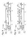
- Fig. 9 depicts a graph, used for explaining the "0" read operation of the circuit shown in Fig. 8.
- Fig. 10 depicts a graph, used for explaining the "1" read operation of the circuit shown in Fig. 8.
- the circuit of the present invention contains the aforesaid first circuit and the second circuit.
- the first circuit supplies the pre-charge voltage to the pre-charge circuit PRE.
- the second circuit supplies a predetermined voltage to the capacitor C S , at the second electrode thereof.
- the term "second electrode" has already been explained with reference to Fig. 1.
- the predetermined voltage from the second circuit is exactly the same as the voltage from the first circuit.
- the output voltages from said first and second circuit are defined as just the middle of the high voltage level developed at the bit line and the low voltage level developed at the same bit line.
- said high voltage level and low voltage level may be selected to be, respectively V CC and V SS of the memory power source. In this case, a dynamic pull-up circuit is necessary. Since the first and second circuit produce the same output voltage, that is 1 ⁇ 2 (V CC - V SS ), these circuits are fabricated as a single voltage divider.
- the circuit of Fig. 8 corresponds to a circuit which contains the above mentioned single voltage divider PS and the above mentioned dynamic pull-up circuits DPU. Referring to Fig. 8, this circuit is different from that of Fig. 5 from the following two view points. Firstly, the output voltage V C being equal to 1 ⁇ 2(V CC - V SS ) from the voltage divider VD, is also applied to the pre-charge circuit PRE. Secondly, the voltage level of both the bit lines BL and BL , appearing during the stand-by status, becomes 1 ⁇ 2V CC , which level 1 ⁇ 2 V CC has been pre-charged by the circuit PR E, and accordingly, the voltage itself of the bit line BL can be utilized as the aforesaid reference voltage V ref .
- the dummy cell DMC can be removed from the circuits illustrated in Figs. 1, 3 and 5, as shown in Fig. 8.
- the dynamic pull-up circuits DPU are connected to the bit lines BL and BL.
- the dummy cell DMC is not illustrated in Fig. 8, this DMC can be left as it is, if necessary, because such cell is available for suppressing undesired noise.
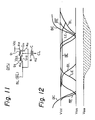
- Fig. 11 illustrates one example of the dynamic pull-up circuit shown in Fig. 8.
- the dynamic pull-up circuit DPU is connected to each of the bit lines BL and BL so as to lead the aforesaid high voltage level of V CC thereto.
- the circuit DPU is comprised of an enhancement type MIS transistor Q 11 , having a gate gl, first and second electrodes ell and e12, a depletion type MIS transistor Q 12 , having a gate g2, first and second electrodes e21 and e22, and a capacitor C, having a first electrode el and a second electrode e2 which receive a clock pulse CL, the first electrodes ell and e21 of both said MIS transistors are connected with the bit line BL (BL), the second electrode e22 of the depletion type MIS transistor, the gate gl of the enhancement type MIS transistor and the first electrode el of the capacitor are commonly connected together, the gate g2 of the depletion type MIS transistor receive
- the aforesaid stand-by status begins from the time t , in which the voltage level of each bit line cannot be changed by, for example a junction-leak current due to the voltage divider VD, and the voltage level 2.25 V is fixedly maintained.
- the word line WL is activated and the aforesaid voltage difference ⁇ V BL between the bit lines BL and BL is created in accordance with the information stored in the memory cell MC.
- the sense amplifier SA is driven so that the low voltage level of one of the bit lines is pulled down toward the level V SS , while, the high voltage level of the other bit line is pulled up toward the level V CC by means of one of the corresponding dynamic pull-up circuits DPU.
- the amplified difference voltage is transferred, via a column line (not shown), to a read-write amplifier (not shown).
- the first one is that no dummy cell DMC is required for constructing the RAM
- the second one is that a high speed read operation is expected, because, the read operation can be commenced immediately after the time t and the third one is that power consumption can be reduced in the RAM, because a very large resistance value of each of the resistors R in the voltage divider VD is allowed.
- the present invention can overcome the other previously mentioned defect, which defect is that error in RAM system often occurs due to change in level of backgate voltage (V BB ) for biassing the substrate, in which the change of V BB is necessarily created in accordance with the voltage change developed at the bit lines BL and BL.
- the circuit construction according to the present invention is very useful for suppressing the change in the backgate voltage V BB .
- the first circuit functions to supply a pre-charge voltage to the pre-charge circuit PRE, and the pre-charge voltage is defined as just the middle of the levels V CC and V SS .
- the previously mentioned second circuit functions to supply a predetermined voltage to the capacitor C S , i.e.
- the predetermined voltage may be chosen from a voltage having the level of V CC , V SS or 1 ⁇ 2 (VCC V SS ).
- VCC V SS 1 ⁇ 2
- Fi g . 14 which will be explained hereinafter, the first circuit is illustrated as a voltage divider VD I having two resistors R'.
- Fig. 12 depicts a first graph, used for explaining the change of V BB .
- the first graph is obtained when the semiconductor memory circuit having a circuit diagram of Fig. 1 or Fig. 3 is used.
- the meanings of respective reference symbols have already been explained.
- the change in the backgate voltage V BB should be noted, which change is indicated by hatched lines surrounded by broken lines. The reason why the voltage V BB changes in such a wide range as illustrated in Fig. 12, will be explained hereinafter.
- the backgate voltage that is, the voltage of the substrate V BB , was determined in the prior art, by an external biassing voltage generator.
- the RAM system does not operate with such an external biassing voltage generator, but, an identical biassing voltage is generated in the RAM system itself, by using a single power source of 5 V (V CC ).
- V CC 5 V
- the bit lines BL and BL are fabricated by diffusion layers, a great amount of PN--junction capacity is created between the bit lines and the substrate. As a result, if a big change in the voltage level occurs in either one of the bit lines, this change of voltage is directly transmitted to the substrate, via the above mentioned large PN-junction capacity.
- V BB changes proportionally to the voltage change of the bit line BL. If such large voltage change occurs in the bit line BL , the voltage level V BB may change in proportion to the voltage of the line BL .
- Fig. 13 depicts a second graph, used for explaining the change of V BB
- the second graph indicates an improvement with respect to the change of V BB shown in Fig. 12.
- the change in V BB is indicated by hatched lines surrounded by a chain-dotted line, and accordingly, the change in V BB shown in Fig. 12, also illustrated in Fig. 13 by a broken line, is relatively minimized. This is why the pre-charge voltage of both the bit lines BL and BL is reduced from the level V CC to the level V C ' which is illustrated in Fig. 13.
- Fig. 14 illustrates a circuit diagram of the other embodiment representing the semiconductor memory circuit according to the present invention.
- the previously explained circuit construction according to the present invention, especially the aforementioned first circuit, is very useful for suppressing change in V BB .
- the first circuit (VD') functions to supply the pre-charge voltage (V C ") to the pre-charge circuit PRE, and the pre-charge voltage is defined as just the middle of the levels V CC and V SS .
- the previously mentioned second circuit functions to supply a predetermined voltage to the capacitor C S , i.e. to its second electrode.
- the predetermined voltage may be chosen from a voltage having the level of V CC , V SS or 1 ⁇ 2 (V CC - V SS ), but in this Fig. 14, the level V CC is chosen.
- the voltage level V C " is determined to be 1 ⁇ 2 (V CC - V SS )
- the change in V BB caused by an upward voltage shift of one bit line, is almost cancelled by the change in V BB , caused by a downward voltage shift of the other bit line.
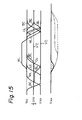
- Fig. 15 depicts a graph, used for explaining the change of V BB , obtained by using the semiconductor memory circuit shown in Fig. 14.
- Fig. 15 depicts a graph, used for explaining the change of V BB , obtained by using the semiconductor memory circuit shown in Fig. 14. In Fig.
- V BB the change in V BB is indicated by hatched lines surrounded by a solid line, and accordingly, the change in V BB illustrated in Figs. 12 and 13, also illustrated in Fig. 15 by a broken line and a chain-dotted line, is considerably minimized.
- the present invention can overcome the aforesaid two defects, and accordingly first the read error, due to the change of the memory power source, cannot occur, and second the change of V BB in the substrate can be stabilized.
- the following three advantages are produced, firstly, no dummy cell is required, secondly, a high speed read operation can be achieved and lastly the power consumption in the voltage divider VD can be reduced.
Landscapes
- Engineering & Computer Science (AREA)
- Microelectronics & Electronic Packaging (AREA)
- Computer Hardware Design (AREA)
- Dram (AREA)
Priority Applications (1)
| Application Number | Priority Date | Filing Date | Title |
|---|---|---|---|
| EP87104318A EP0239913B2 (de) | 1980-10-22 | 1981-10-22 | Halbleiterspeicherschaltung |
Applications Claiming Priority (4)
| Application Number | Priority Date | Filing Date | Title |
|---|---|---|---|
| JP147773/80 | 1980-10-22 | ||
| JP55147771A JPS5771579A (en) | 1980-10-22 | 1980-10-22 | Semiconductor memory device |
| JP147771/80 | 1980-10-22 | ||
| JP55147773A JPS5771580A (en) | 1980-10-22 | 1980-10-22 | Semiconductor memory device |
Related Child Applications (1)
| Application Number | Title | Priority Date | Filing Date |
|---|---|---|---|
| EP87104318.8 Division-Into | 1987-03-24 |
Publications (3)
| Publication Number | Publication Date |
|---|---|
| EP0050529A2 true EP0050529A2 (de) | 1982-04-28 |
| EP0050529A3 EP0050529A3 (en) | 1984-10-10 |
| EP0050529B1 EP0050529B1 (de) | 1988-01-07 |
Family
ID=26478221
Family Applications (1)
| Application Number | Title | Priority Date | Filing Date |
|---|---|---|---|
| EP81304967A Expired EP0050529B1 (de) | 1980-10-22 | 1981-10-22 | Halbleiterspeicherschaltung |
Country Status (4)
| Country | Link |
|---|---|
| US (1) | US4458336A (de) |
| EP (1) | EP0050529B1 (de) |
| DE (2) | DE3176601D1 (de) |
| IE (1) | IE53512B1 (de) |
Cited By (9)
| Publication number | Priority date | Publication date | Assignee | Title |
|---|---|---|---|---|
| FR2533348A1 (fr) * | 1982-09-22 | 1984-03-23 | Hitachi Ltd | Dispositif de memoire a semiconducteurs |
| EP0113187A3 (en) * | 1982-12-01 | 1986-08-20 | Fujitsu Limited | A dynamic semiconductor memory device |
| GB2184311A (en) * | 1984-02-22 | 1987-06-17 | Intel Corp | Metal-oxide-semiconductor dynamic ram |
| EP0187246A3 (de) * | 1984-12-28 | 1987-09-16 | Kabushiki Kaisha Toshiba | Bitzeilenvorladungsschaltung eines Halbleiterspeichers |
| EP0200500A3 (de) * | 1985-04-26 | 1989-03-08 | Advanced Micro Devices, Inc. | CMOS-Speichervorspannungssystem |
| EP0326708A3 (de) * | 1987-12-25 | 1990-08-08 | Nec Corporation | Halbleiterspeicheranordnung mit verbesserter Bitzeilenvorladungsschaltung |
| EP0383009A3 (de) * | 1989-01-27 | 1991-08-07 | Kabushiki Kaisha Toshiba | Leseverstärker für einen Halbleiter-Speicher |
| GB2242767A (en) * | 1990-04-06 | 1991-10-09 | Mosaid Inc | Precharging DRAM bit lines to half supply potential |
| EP0622800A3 (de) * | 1993-04-28 | 1995-09-20 | Fujitsu Ltd | Halbleiterspeicheranordnung. |
Families Citing this family (9)
| Publication number | Priority date | Publication date | Assignee | Title |
|---|---|---|---|---|
| US4617652A (en) * | 1979-01-24 | 1986-10-14 | Xicor, Inc. | Integrated high voltage distribution and control systems |
| JPS58121195A (ja) * | 1982-01-13 | 1983-07-19 | Nec Corp | プリチヤ−ジ信号発生回路 |
| US4658382A (en) * | 1984-07-11 | 1987-04-14 | Texas Instruments Incorporated | Dynamic memory with improved dummy cell circuitry |
| JPS6134619A (ja) * | 1984-07-26 | 1986-02-18 | Mitsubishi Electric Corp | Mosトランジスタ回路 |
| US5687109A (en) * | 1988-05-31 | 1997-11-11 | Micron Technology, Inc. | Integrated circuit module having on-chip surge capacitors |
| JPH05342873A (ja) * | 1992-06-10 | 1993-12-24 | Nec Corp | 半導体記憶装置 |
| KR100214462B1 (ko) * | 1995-11-27 | 1999-08-02 | 구본준 | 반도체메모리셀의 라이트 방법 |
| US7145819B2 (en) * | 2001-06-11 | 2006-12-05 | Analog Devices, Inc. | Method and apparatus for integrated circuit with DRAM |
| US9786345B1 (en) * | 2016-09-16 | 2017-10-10 | Micron Technology, Inc. | Compensation for threshold voltage variation of memory cell components |
Family Cites Families (4)
| Publication number | Priority date | Publication date | Assignee | Title |
|---|---|---|---|---|
| US4004284A (en) * | 1975-03-05 | 1977-01-18 | Teletype Corporation | Binary voltage-differential sensing circuits, and sense/refresh amplifier circuits for random-access memories |
| US4045783A (en) * | 1976-04-12 | 1977-08-30 | Standard Microsystems Corporation | Mos one transistor cell ram having divided and balanced bit lines, coupled by regenerative flip-flop sense amplifiers, and balanced access circuitry |
| US4195357A (en) * | 1978-06-15 | 1980-03-25 | Texas Instruments Incorporated | Median spaced dummy cell layout for MOS random access memory |
| US4291393A (en) * | 1980-02-11 | 1981-09-22 | Mostek Corporation | Active refresh circuit for dynamic MOS circuits |
-
1981
- 1981-10-21 US US06/313,616 patent/US4458336A/en not_active Expired - Lifetime
- 1981-10-22 DE DE8181304967T patent/DE3176601D1/de not_active Expired
- 1981-10-22 DE DE8787104318T patent/DE3177221D1/de not_active Expired - Lifetime
- 1981-10-22 IE IE2483/81A patent/IE53512B1/en not_active IP Right Cessation
- 1981-10-22 EP EP81304967A patent/EP0050529B1/de not_active Expired
Cited By (11)
| Publication number | Priority date | Publication date | Assignee | Title |
|---|---|---|---|---|
| FR2533348A1 (fr) * | 1982-09-22 | 1984-03-23 | Hitachi Ltd | Dispositif de memoire a semiconducteurs |
| GB2128430A (en) * | 1982-09-22 | 1984-04-26 | Hitachi Ltd | A semiconductor memory device |
| EP0113187A3 (en) * | 1982-12-01 | 1986-08-20 | Fujitsu Limited | A dynamic semiconductor memory device |
| GB2184311A (en) * | 1984-02-22 | 1987-06-17 | Intel Corp | Metal-oxide-semiconductor dynamic ram |
| EP0187246A3 (de) * | 1984-12-28 | 1987-09-16 | Kabushiki Kaisha Toshiba | Bitzeilenvorladungsschaltung eines Halbleiterspeichers |
| EP0200500A3 (de) * | 1985-04-26 | 1989-03-08 | Advanced Micro Devices, Inc. | CMOS-Speichervorspannungssystem |
| EP0326708A3 (de) * | 1987-12-25 | 1990-08-08 | Nec Corporation | Halbleiterspeicheranordnung mit verbesserter Bitzeilenvorladungsschaltung |
| EP0383009A3 (de) * | 1989-01-27 | 1991-08-07 | Kabushiki Kaisha Toshiba | Leseverstärker für einen Halbleiter-Speicher |
| GB2242767A (en) * | 1990-04-06 | 1991-10-09 | Mosaid Inc | Precharging DRAM bit lines to half supply potential |
| EP0622800A3 (de) * | 1993-04-28 | 1995-09-20 | Fujitsu Ltd | Halbleiterspeicheranordnung. |
| US5544109A (en) * | 1993-04-28 | 1996-08-06 | Fujitsu Limited | Semiconductor memory device |
Also Published As
| Publication number | Publication date |
|---|---|
| IE812483L (en) | 1982-04-22 |
| DE3177221D1 (de) | 1990-11-15 |
| EP0050529A3 (en) | 1984-10-10 |
| EP0050529B1 (de) | 1988-01-07 |
| DE3176601D1 (en) | 1988-02-11 |
| US4458336A (en) | 1984-07-03 |
| IE53512B1 (en) | 1988-12-07 |
Similar Documents
| Publication | Publication Date | Title |
|---|---|---|
| EP0050529B1 (de) | Halbleiterspeicherschaltung | |
| EP0100908B1 (de) | Halbleiterspeicheranordnung mit mehreren Ladungsspeichertypzellen | |
| US4563754A (en) | Static-type random-access memory device | |
| EP0077935B1 (de) | Dynamische Speicheranordnung | |
| JPH0512866A (ja) | ダイナミツク型半導体記憶装置 | |
| KR950001126B1 (ko) | 메모리 회로 | |
| US7209399B2 (en) | Circuit and method of driving bitlines of integrated circuit memory using improved precharge scheme and sense-amplification scheme | |
| US5491435A (en) | Data sensing circuit with additional capacitors for eliminating parasitic capacitance difference between sensing control nodes of sense amplifier | |
| EP0449204A2 (de) | Halbleiterspeicheranordnung von dynamischem Typus | |
| EP0073677B1 (de) | MIS Transistorschaltung mit einer Spannungshalteschaltung | |
| US4802128A (en) | Bit line driver | |
| KR19980064537A (ko) | 반도체 기억장치 | |
| US4409672A (en) | Dynamic semiconductor memory device | |
| US4858193A (en) | Preamplification method and apparatus for dram sense amplifiers | |
| US5777934A (en) | Semiconductor memory device with variable plate voltage generator | |
| EP0040001A2 (de) | Dynamische Halbleiterspeicheranordnung mit reduzierten Taktimpulsen | |
| EP0239913B1 (de) | Halbleiterspeicherschaltung | |
| EP0318927A2 (de) | Halbleiterspeicher mit Abtastanordnung (ohne Funktionsstörung) | |
| KR900004634B1 (ko) | 모스 다이나믹 램의 더미 워드선 구동회로 | |
| EP0318094B1 (de) | Integrierte Speicherschaltung mit innerer Speisespannungsregelung | |
| JP2001229671A (ja) | 半導体記憶装置 | |
| JPH06309872A (ja) | 半導体記憶装置 | |
| JP3824370B2 (ja) | 半導体装置 | |
| JPS6137707B2 (de) | ||
| JPS63894A (ja) | メモリ |
Legal Events
| Date | Code | Title | Description |
|---|---|---|---|
| PUAI | Public reference made under article 153(3) epc to a published international application that has entered the european phase |
Free format text: ORIGINAL CODE: 0009012 |
|
| AK | Designated contracting states |
Designated state(s): DE FR GB NL |
|
| RBV | Designated contracting states (corrected) |
Designated state(s): DE FR GB NL |
|
| PUAL | Search report despatched |
Free format text: ORIGINAL CODE: 0009013 |
|
| AK | Designated contracting states |
Designated state(s): DE FR GB NL |
|
| 17P | Request for examination filed |
Effective date: 19841101 |
|
| GRAA | (expected) grant |
Free format text: ORIGINAL CODE: 0009210 |
|
| AK | Designated contracting states |
Kind code of ref document: B1 Designated state(s): DE FR GB NL |
|
| REF | Corresponds to: |
Ref document number: 3176601 Country of ref document: DE Date of ref document: 19880211 |
|
| ET | Fr: translation filed | ||
| PLBE | No opposition filed within time limit |
Free format text: ORIGINAL CODE: 0009261 |
|
| STAA | Information on the status of an ep patent application or granted ep patent |
Free format text: STATUS: NO OPPOSITION FILED WITHIN TIME LIMIT |
|
| 26N | No opposition filed | ||
| PGFP | Annual fee paid to national office [announced via postgrant information from national office to epo] |
Ref country code: FR Payment date: 20001010 Year of fee payment: 20 |
|
| PGFP | Annual fee paid to national office [announced via postgrant information from national office to epo] |
Ref country code: DE Payment date: 20001016 Year of fee payment: 20 |
|
| PGFP | Annual fee paid to national office [announced via postgrant information from national office to epo] |
Ref country code: GB Payment date: 20001018 Year of fee payment: 20 |
|
| PGFP | Annual fee paid to national office [announced via postgrant information from national office to epo] |
Ref country code: NL Payment date: 20001026 Year of fee payment: 20 |
|
| PG25 | Lapsed in a contracting state [announced via postgrant information from national office to epo] |
Ref country code: GB Free format text: LAPSE BECAUSE OF EXPIRATION OF PROTECTION Effective date: 20011021 |
|
| PG25 | Lapsed in a contracting state [announced via postgrant information from national office to epo] |
Ref country code: NL Free format text: LAPSE BECAUSE OF EXPIRATION OF PROTECTION Effective date: 20011022 |
|
| REG | Reference to a national code |
Ref country code: GB Ref legal event code: PE20 Effective date: 20011021 |
|
| NLV7 | Nl: ceased due to reaching the maximum lifetime of a patent |
Effective date: 20011022 |