EP0050903A1 - Procédé de fabrication de modules de circuits multicouches en céramique - Google Patents
Procédé de fabrication de modules de circuits multicouches en céramique Download PDFInfo
- Publication number
- EP0050903A1 EP0050903A1 EP81201197A EP81201197A EP0050903A1 EP 0050903 A1 EP0050903 A1 EP 0050903A1 EP 81201197 A EP81201197 A EP 81201197A EP 81201197 A EP81201197 A EP 81201197A EP 0050903 A1 EP0050903 A1 EP 0050903A1
- Authority
- EP
- European Patent Office
- Prior art keywords
- binder
- ceramic
- conductive paste
- module
- process according
- Prior art date
- Legal status (The legal status is an assumption and is not a legal conclusion. Google has not performed a legal analysis and makes no representation as to the accuracy of the status listed.)
- Granted
Links
Images



Classifications
-
- C—CHEMISTRY; METALLURGY
- C04—CEMENTS; CONCRETE; ARTIFICIAL STONE; CERAMICS; REFRACTORIES
- C04B—LIME, MAGNESIA; SLAG; CEMENTS; COMPOSITIONS THEREOF, e.g. MORTARS, CONCRETE OR LIKE BUILDING MATERIALS; ARTIFICIAL STONE; CERAMICS; REFRACTORIES; TREATMENT OF NATURAL STONE
- C04B41/00—After-treatment of mortars, concrete, artificial stone or ceramics; Treatment of natural stone
- C04B41/009—After-treatment of mortars, concrete, artificial stone or ceramics; Treatment of natural stone characterised by the material treated
-
- C—CHEMISTRY; METALLURGY
- C04—CEMENTS; CONCRETE; ARTIFICIAL STONE; CERAMICS; REFRACTORIES
- C04B—LIME, MAGNESIA; SLAG; CEMENTS; COMPOSITIONS THEREOF, e.g. MORTARS, CONCRETE OR LIKE BUILDING MATERIALS; ARTIFICIAL STONE; CERAMICS; REFRACTORIES; TREATMENT OF NATURAL STONE
- C04B35/00—Shaped ceramic products characterised by their composition; Ceramics compositions; Processing powders of inorganic compounds preparatory to the manufacturing of ceramic products
- C04B35/622—Forming processes; Processing powders of inorganic compounds preparatory to the manufacturing of ceramic products
- C04B35/626—Preparing or treating the powders individually or as batches ; preparing or treating macroscopic reinforcing agents for ceramic products, e.g. fibres; mechanical aspects section B
- C04B35/63—Preparing or treating the powders individually or as batches ; preparing or treating macroscopic reinforcing agents for ceramic products, e.g. fibres; mechanical aspects section B using additives specially adapted for forming the products, e.g.. binder binders
- C04B35/632—Organic additives
-
- C—CHEMISTRY; METALLURGY
- C04—CEMENTS; CONCRETE; ARTIFICIAL STONE; CERAMICS; REFRACTORIES
- C04B—LIME, MAGNESIA; SLAG; CEMENTS; COMPOSITIONS THEREOF, e.g. MORTARS, CONCRETE OR LIKE BUILDING MATERIALS; ARTIFICIAL STONE; CERAMICS; REFRACTORIES; TREATMENT OF NATURAL STONE
- C04B35/00—Shaped ceramic products characterised by their composition; Ceramics compositions; Processing powders of inorganic compounds preparatory to the manufacturing of ceramic products
- C04B35/622—Forming processes; Processing powders of inorganic compounds preparatory to the manufacturing of ceramic products
- C04B35/626—Preparing or treating the powders individually or as batches ; preparing or treating macroscopic reinforcing agents for ceramic products, e.g. fibres; mechanical aspects section B
- C04B35/63—Preparing or treating the powders individually or as batches ; preparing or treating macroscopic reinforcing agents for ceramic products, e.g. fibres; mechanical aspects section B using additives specially adapted for forming the products, e.g.. binder binders
- C04B35/638—Removal thereof
-
- C—CHEMISTRY; METALLURGY
- C04—CEMENTS; CONCRETE; ARTIFICIAL STONE; CERAMICS; REFRACTORIES
- C04B—LIME, MAGNESIA; SLAG; CEMENTS; COMPOSITIONS THEREOF, e.g. MORTARS, CONCRETE OR LIKE BUILDING MATERIALS; ARTIFICIAL STONE; CERAMICS; REFRACTORIES; TREATMENT OF NATURAL STONE
- C04B41/00—After-treatment of mortars, concrete, artificial stone or ceramics; Treatment of natural stone
- C04B41/45—Coating or impregnating, e.g. injection in masonry, partial coating of green or fired ceramics, organic coating compositions for adhering together two concrete elements
- C04B41/50—Coating or impregnating, e.g. injection in masonry, partial coating of green or fired ceramics, organic coating compositions for adhering together two concrete elements with inorganic materials
- C04B41/51—Metallising, e.g. infiltration of sintered ceramic preforms with molten metal
-
- C—CHEMISTRY; METALLURGY
- C04—CEMENTS; CONCRETE; ARTIFICIAL STONE; CERAMICS; REFRACTORIES
- C04B—LIME, MAGNESIA; SLAG; CEMENTS; COMPOSITIONS THEREOF, e.g. MORTARS, CONCRETE OR LIKE BUILDING MATERIALS; ARTIFICIAL STONE; CERAMICS; REFRACTORIES; TREATMENT OF NATURAL STONE
- C04B41/00—After-treatment of mortars, concrete, artificial stone or ceramics; Treatment of natural stone
- C04B41/53—After-treatment of mortars, concrete, artificial stone or ceramics; Treatment of natural stone involving the removal of at least part of the materials of the treated article, e.g. etching, drying of hardened concrete
-
- C—CHEMISTRY; METALLURGY
- C04—CEMENTS; CONCRETE; ARTIFICIAL STONE; CERAMICS; REFRACTORIES
- C04B—LIME, MAGNESIA; SLAG; CEMENTS; COMPOSITIONS THEREOF, e.g. MORTARS, CONCRETE OR LIKE BUILDING MATERIALS; ARTIFICIAL STONE; CERAMICS; REFRACTORIES; TREATMENT OF NATURAL STONE
- C04B41/00—After-treatment of mortars, concrete, artificial stone or ceramics; Treatment of natural stone
- C04B41/80—After-treatment of mortars, concrete, artificial stone or ceramics; Treatment of natural stone of only ceramics
- C04B41/81—Coating or impregnation
- C04B41/85—Coating or impregnation with inorganic materials
- C04B41/88—Metals
-
- C—CHEMISTRY; METALLURGY
- C04—CEMENTS; CONCRETE; ARTIFICIAL STONE; CERAMICS; REFRACTORIES
- C04B—LIME, MAGNESIA; SLAG; CEMENTS; COMPOSITIONS THEREOF, e.g. MORTARS, CONCRETE OR LIKE BUILDING MATERIALS; ARTIFICIAL STONE; CERAMICS; REFRACTORIES; TREATMENT OF NATURAL STONE
- C04B41/00—After-treatment of mortars, concrete, artificial stone or ceramics; Treatment of natural stone
- C04B41/80—After-treatment of mortars, concrete, artificial stone or ceramics; Treatment of natural stone of only ceramics
- C04B41/91—After-treatment of mortars, concrete, artificial stone or ceramics; Treatment of natural stone of only ceramics involving the removal of part of the materials of the treated articles, e.g. etching
-
- H—ELECTRICITY
- H10—SEMICONDUCTOR DEVICES; ELECTRIC SOLID-STATE DEVICES NOT OTHERWISE PROVIDED FOR
- H10W—GENERIC PACKAGES, INTERCONNECTIONS, CONNECTORS OR OTHER CONSTRUCTIONAL DETAILS OF DEVICES COVERED BY CLASS H10
- H10W70/00—Package substrates; Interposers; Redistribution layers [RDL]
- H10W70/01—Manufacture or treatment
- H10W70/05—Manufacture or treatment of insulating or insulated package substrates, or of interposers, or of redistribution layers
- H10W70/098—Applying pastes or inks, e.g. screen printing
-
- H—ELECTRICITY
- H05—ELECTRIC TECHNIQUES NOT OTHERWISE PROVIDED FOR
- H05K—PRINTED CIRCUITS; CASINGS OR CONSTRUCTIONAL DETAILS OF ELECTRIC APPARATUS; MANUFACTURE OF ASSEMBLAGES OF ELECTRICAL COMPONENTS
- H05K1/00—Printed circuits
- H05K1/02—Details
- H05K1/03—Use of materials for the substrate
- H05K1/0306—Inorganic insulating substrates, e.g. ceramic, glass
-
- H—ELECTRICITY
- H05—ELECTRIC TECHNIQUES NOT OTHERWISE PROVIDED FOR
- H05K—PRINTED CIRCUITS; CASINGS OR CONSTRUCTIONAL DETAILS OF ELECTRIC APPARATUS; MANUFACTURE OF ASSEMBLAGES OF ELECTRICAL COMPONENTS
- H05K3/00—Apparatus or processes for manufacturing printed circuits
- H05K3/0011—Working of insulating substrates or insulating layers
- H05K3/0014—Shaping of the substrate, e.g. by moulding
-
- H—ELECTRICITY
- H05—ELECTRIC TECHNIQUES NOT OTHERWISE PROVIDED FOR
- H05K—PRINTED CIRCUITS; CASINGS OR CONSTRUCTIONAL DETAILS OF ELECTRIC APPARATUS; MANUFACTURE OF ASSEMBLAGES OF ELECTRICAL COMPONENTS
- H05K3/00—Apparatus or processes for manufacturing printed circuits
- H05K3/46—Manufacturing multilayer circuits
- H05K3/4611—Manufacturing multilayer circuits by laminating two or more circuit boards
-
- H—ELECTRICITY
- H05—ELECTRIC TECHNIQUES NOT OTHERWISE PROVIDED FOR
- H05K—PRINTED CIRCUITS; CASINGS OR CONSTRUCTIONAL DETAILS OF ELECTRIC APPARATUS; MANUFACTURE OF ASSEMBLAGES OF ELECTRICAL COMPONENTS
- H05K3/00—Apparatus or processes for manufacturing printed circuits
- H05K3/46—Manufacturing multilayer circuits
- H05K3/4611—Manufacturing multilayer circuits by laminating two or more circuit boards
- H05K3/4626—Manufacturing multilayer circuits by laminating two or more circuit boards characterised by the insulating layers or materials
- H05K3/4629—Manufacturing multilayer circuits by laminating two or more circuit boards characterised by the insulating layers or materials laminating inorganic sheets comprising printed circuits, e.g. green ceramic sheets
-
- H—ELECTRICITY
- H10—SEMICONDUCTOR DEVICES; ELECTRIC SOLID-STATE DEVICES NOT OTHERWISE PROVIDED FOR
- H10W—GENERIC PACKAGES, INTERCONNECTIONS, CONNECTORS OR OTHER CONSTRUCTIONAL DETAILS OF DEVICES COVERED BY CLASS H10
- H10W90/00—Package configurations
- H10W90/701—Package configurations characterised by the relative positions of pads or connectors relative to package parts
- H10W90/751—Package configurations characterised by the relative positions of pads or connectors relative to package parts of bond wires
- H10W90/754—Package configurations characterised by the relative positions of pads or connectors relative to package parts of bond wires between a chip and a stacked insulating package substrate, interposer or RDL
Definitions
- Carriers for integrated circuits have heretofore been made by layering ceramic sheets and cutting these sheets into approximately one to two inch squares. The squares are thereafter punched with a hole press to produce the required vias and aligning holes used in stacked multilayer ceramic (MLC) modules. Conductive pastes are then applied to each ceramic sheet and the sheets are placed one on top of another, laminated together and sintered. Problems have arisen caused by cracked chip carriers, improper layering of the paste between ceramic sheets, poor control of circuit patterns and poor control of via locations. It is not unusual to have up to 70 percent of ceramic sheets destroyed because of these problems.
- MLC multilayer ceramic
- a ceramic injection moldable mixture is prepared by mixing approximately 60 to 90 percent by weight of particles, approximately 0.2 to 4 microns in diameter, taken from the following group :
- the resulting mixture is injected into molds 10 as shown in FIG. 4 through inlet 12.
- the molds contain ridges 14 and pins 16 as well as a flat surface 18. Additionally, the mold has aligning knobs 20.
- a mold 10 containing the mixture of particulate and binder is cooled to a temperature below the melting point of the binder, and the resulting "green body" is removed from the mold.
- the exact size of the molds and therefore the resulting "green body” will vary according to the intended final size of the ceramic layer.
- the mold may be 15-20 % larger than the ceramic layer to allow for a precisely calculated shrinkage.
- a square of 1 to 2 inches (2.5 to 5 cm) is customarily used for each layer in an MLC module.
- Each mold will be deep enough to make ceramic layers from 0.2 to 0.5 millimeter thick.
- FIG. 6 shows the raised portion 14 of the mold 10 and the pin 16 in elevation.
- the grooves and vias produced by the ridge 14 and the pin 16, respectively, provide for increased density of conductive paths throughout each layer of ceramic.
- the raised portion 14 is about 0.10 mm wide with a gap of at least 0.10 mm between each raised portion 14. The length depends on the contact distance to be covered.
- the posts 16 are 0.05 to 0.15 mm in diameter with the preferred diameter being about 0.10 mm.
- Conductive-pastes containing refractory metals such as molybdenum or tungsten, nonprecious metals such as copper or nickel, precious metals such as gold, palladium, silver, platinum or alloys thereof are then applied to the ceramic layers to form a wiring pattern in accordance with a predetermined system for each ceramic layer.
- Choice of conductive paste depends upon the firing temperature of the ceramic employed. It is important to notefuat the conductor in the paste may sinter but must not melt at or below the firing temperature of the ceramic.
- molybdenum, tungsten or platinum may be used with alumina ceramics and gold, silver, copper or nickel may be used with barium titanate ceramics.
- Methods of applying the paste can include screen printing, spray coating, dip or brush coating, vapor deposition or doctor blading. Additional paste compositions including additives therefore are set forth in U.S. Patent 4,101,710. The disclosure is herein incorporated by reference.
- the paste is applied to the ceramic layers through metal masks directly into the grooves 32 and down through the vias 30 as shown in FIGS. 1, 2, and 3.
- Stacks of the ceramic layers with the required configurations of conductors, layer-to-layer connections and reference and power planes are laminated together to form individual modules.
- the organic oil or wax binder is stripped from the "green body” ceramic layers with a solvent such as cumene, trichloroethylene or FREON TF after applying the conductive pastes and laminating the layers together.
- a solvent such as cumene, trichloroethylene or FREON TF
- the process of stripping the binder is set forth in U.S. Patent 4,197,118. It involves exposing the "green body” first to solvent in the gaseous state and then in the liquid state.
- the ceramic "green” layers are fired at 900 C to 1550°C Vsinter to the ceramic. It is preferred, using an alumina ceramic and a tungsten thick film paste, to fire the module at about 1550 ° C.
- Metallized pads for subsequent integrated circuit attachment can be applied before or after sintering with proper choice of metallization.
- Refractory metals such as tungsten or molybdenum require plating to make them compatible with integrated circuits.
- the modules can contain up to 23 or more ceramic layers and as many integrated circuits as space on each module permits.
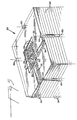
- the completed module with semi-conductors 26 in place is shown in FIG. 5.
- the semi-conductors are in electrical contact through wires 28 to the conductive paths 32 in each layer 24 of the module 22.
- a particle mixture is prepared using alumina (70 %) and Carnauba wax (30 %) as binder.
- the alumina has an average particle size of 0.6 micron and a particle size range from about 3 microns to 0.2 microns.
- the materials are mixed together at a temperature above the melting point of the binder.
- the binder is then allowed to cool and form the raw material for the forming process.
- the mixture is subsequently heated and formed in a mold as shown in FIG. 4 with pressure into the desired layer configuration.
- the layer then hardens by cooling to form the green body layer.
- the green body sheets are then metallized by screen printing a conductive paste containing tungsten.
- the metallized green sheets are stacked using alignment holes 20 to provide multilayers.
- the multilayers are laminated together at 75 ° C with a pressure of approximately 25 megapascals.
- the laminated green body is placed in a container and slowly heated to the melting point (85 0 C) of the Carnauba wax. Cumene solvent vapors are introduced into the container to strip out the Carnauba wax binder. The solvent is entered into the chamber at a rate sufficiently slow so that the swelling caused by the solvent on the binder is not sufficient to cause cracking or breaking of the green body. Layer configuration will dictate the time for gaseous treatment.
- the green body is placed in a liquid solution of the same solvent at a temperature above the melting point of the binder whereby the remaining binder is removed. It should be understood that some binder remains to provide strength for the laminated green body.
- the remaining binder and solvent (if any remains) are removed by a low temperature burn.
- the laminated green body is placed in an oven and-the temperature is raised slowly to a point slightly above the boiling point of the binder.
- the temperature is then raised to 100° C for one hour to remove any water which may have entered into the green body.
- the temperature is then raised to 350 C in a wet dissociated ammonia atmosphere for three days to burn out all remaining binder.
- the sample is then kiln fired in dissociated ammonia atmosphere at 1540°C for one hour and then cooled.
- the heating and cooling cycle takes 24 hours, 18 hours of which are required to reach the 15400C sintering temperature.
- the resultant module has excellent dimensions and electrical circuitry.
- Example I The steps of Example I are repeated except substituting a binder system of soybean oil and Carnauba wax.
- the leaching agent if Freon TF.
- the greer. body is metallized, slow burned and fired as described in Example I to form an MLC module.
- Example II The steps of Example II are repeated using trichloroethylene to leach out the Carnauba wax binder and provide an essentially binder free green body.
- the burn off step is eliminated and after firing as described above an MLC module is produced.
- Example I is repeated using particulate mixtures as follows :
- Example I The particulate and binder of Example I is prepared as described, injection molded layers are metallized and compression laminated together.
- the laminate is slowly heated to 400°C in a wet dissociated ammonia atmosphere and held at this temperature for up to 12 hours to form a bisque.
- the temperature is then raised to 1540°C in a dissociated ammonia atmosphere to sinter the particles.
- An MLC module is produced.
- Example I The steps of Example I are repeated except that the green body is metallized by doctor blading. An MLC module is produced.
- Example I The steps of Example I are repeated except that 15 % polyethylene binder with a melt index of 14 and 15 % soybean oil as plasticizer are substituted for the Carnauba wax. The same heating temperature of 85°C is used with cumene solvent vapors to strip out the soybean oil. The resulting module has excellent dimensions and electrical circuitry.
Landscapes
- Chemical & Material Sciences (AREA)
- Engineering & Computer Science (AREA)
- Ceramic Engineering (AREA)
- Materials Engineering (AREA)
- Structural Engineering (AREA)
- Organic Chemistry (AREA)
- Inorganic Chemistry (AREA)
- Manufacturing & Machinery (AREA)
- Production Of Multi-Layered Print Wiring Board (AREA)
- Coupling Device And Connection With Printed Circuit (AREA)
Priority Applications (1)
| Application Number | Priority Date | Filing Date | Title |
|---|---|---|---|
| AT81201197T ATE17912T1 (de) | 1980-10-28 | 1981-10-27 | Verfahren zur herstellung mehrschichtiger keramischer chiptraeger-moduln. |
Applications Claiming Priority (4)
| Application Number | Priority Date | Filing Date | Title |
|---|---|---|---|
| US20146980A | 1980-10-28 | 1980-10-28 | |
| US06/307,657 US4345955A (en) | 1980-10-28 | 1981-10-02 | Process for manufacturing multilayer ceramic chip carrier modules |
| US307657 | 1981-10-02 | ||
| US201469 | 1994-02-25 |
Publications (2)
| Publication Number | Publication Date |
|---|---|
| EP0050903A1 true EP0050903A1 (fr) | 1982-05-05 |
| EP0050903B1 EP0050903B1 (fr) | 1986-02-05 |
Family
ID=26896779
Family Applications (1)
| Application Number | Title | Priority Date | Filing Date |
|---|---|---|---|
| EP81201197A Expired EP0050903B1 (fr) | 1980-10-28 | 1981-10-27 | Procédé de fabrication de modules de circuits multicouches en céramique |
Country Status (8)
| Country | Link |
|---|---|
| US (1) | US4345955A (fr) |
| EP (1) | EP0050903B1 (fr) |
| BR (1) | BR8106873A (fr) |
| CA (1) | CA1167979A (fr) |
| DE (1) | DE3173737D1 (fr) |
| DK (1) | DK474181A (fr) |
| ES (1) | ES8206916A1 (fr) |
| NO (1) | NO813626L (fr) |
Cited By (10)
| Publication number | Priority date | Publication date | Assignee | Title |
|---|---|---|---|---|
| EP0064872A3 (fr) * | 1981-05-09 | 1983-08-31 | Hitachi, Ltd. | Plaquettes céramiques à circuits imprimés |
| FR2558763A1 (fr) * | 1984-01-27 | 1985-08-02 | Thomson Csf | Procede de fabrication d'un substrat ceramique, avec plots de connexion electriques transversaux |
| EP0133917A3 (en) * | 1983-08-08 | 1987-03-25 | International Business Machines Corporation | Process for forming a pattern of electrically conductive lines on the top of a ceramic substrate |
| EP0144046A3 (en) * | 1983-11-30 | 1987-07-22 | International Business Machines Corporation | Process for forming a mettallurgical pattern with a densified surface on or in a sintered dielectric substrate |
| DE3630066C1 (de) * | 1986-09-04 | 1988-02-04 | Heraeus Gmbh W C | Verfahren zur Herstellung von gesinterten metallisierten Aluminiumnitrid-Keramikkoerpern |
| EP0220959A3 (en) * | 1985-10-29 | 1989-12-20 | Nec Corporation | Ceramic electronic device and method of manufacturing the same |
| FR2638594A1 (fr) * | 1988-11-03 | 1990-05-04 | Cartier Systemes G | Procede de realisation d'un circuit electrique de puissance monocouche ou multicouches, et circuit obtenu par ce procede |
| EP0400332A3 (fr) * | 1989-06-02 | 1992-03-11 | International Business Machines Corporation | Méthode de fabrication d'un assemblage d'interconnexion sur une plaque multicouche utilisant des pellicules minces |
| EP0520434A1 (fr) * | 1991-06-26 | 1992-12-30 | Hughes Aircraft Company | Emballage intégré de type emboitable pour dispositifs sémi-conducteurs avec flip chip et pour circuits |
| WO1997040529A1 (fr) * | 1996-04-20 | 1997-10-30 | Robert Bosch Gmbh | Procede de fabrication d'un substrat ceramique a couches multiples |
Families Citing this family (19)
| Publication number | Priority date | Publication date | Assignee | Title |
|---|---|---|---|---|
| JPS5820160B2 (ja) * | 1978-06-17 | 1983-04-21 | 日本碍子株式会社 | メタライズ層を備えたセラミツクス体 |
| US4504340A (en) * | 1983-07-26 | 1985-03-12 | International Business Machines Corporation | Material and process set for fabrication of molecular matrix print head |
| JPS6047495A (ja) * | 1983-08-25 | 1985-03-14 | 株式会社日立製作所 | セラミツク配線基板 |
| US4727410A (en) * | 1983-11-23 | 1988-02-23 | Cabot Technical Ceramics, Inc. | High density integrated circuit package |
| US4539058A (en) * | 1983-12-12 | 1985-09-03 | International Business Machines Corporation | Forming multilayer ceramic substrates from large area green sheets |
| JPS61155243A (ja) * | 1984-12-28 | 1986-07-14 | 富士通株式会社 | グリ−ンシ−ト組成物 |
| JPH0632355B2 (ja) * | 1986-01-27 | 1994-04-27 | 株式会社日立製作所 | セラミツク配線基板とその製造方法 |
| GB8602331D0 (en) * | 1986-01-30 | 1986-03-05 | Ici Plc | Multilayer systems |
| US4767479A (en) * | 1987-09-21 | 1988-08-30 | United Technologies Corporation | Method for bonding ceramic casting cores |
| US4765950A (en) * | 1987-10-07 | 1988-08-23 | Risi Industries, Inc. | Process for fabricating parts from particulate material |
| US4929575A (en) * | 1988-03-21 | 1990-05-29 | The Dow Chemical Company | Melt processable, green, ceramic precursor powder |
| JP2761776B2 (ja) * | 1989-10-25 | 1998-06-04 | Ii Ai Deyuhon De Nimoasu Ando Co | 多層回路板の製造方法 |
| US5240671A (en) * | 1992-06-01 | 1993-08-31 | Microelectronics And Computer Technology Corporation | Method of forming recessed patterns in insulating substrates |
| US5340510A (en) * | 1993-04-05 | 1994-08-23 | Materials Systems Incorporated | Method for making piezoelectric ceramic/polymer composite transducers |
| US6214523B1 (en) * | 1998-01-09 | 2001-04-10 | International Business Machines Corporation | Pattern formation by removal of paste material |
| JP2004186395A (ja) * | 2002-12-03 | 2004-07-02 | Fujitsu Ltd | セラミック基板の製造方法 |
| DE102009013021A1 (de) * | 2009-03-16 | 2010-09-23 | Gkn Sinter Metals Holding Gmbh | Schmiermittel für die Pulvermetallurgie |
| DE102013200281A1 (de) * | 2013-01-11 | 2014-07-17 | Robert Bosch Gmbh | Verfahren zum Herstellen einer Aufnahme für ein Sensorelement |
| US11274065B2 (en) * | 2018-06-13 | 2022-03-15 | Fuelcell Energy, Inc. | Ceramic felt material for high-temperature fuel cells |
Citations (4)
| Publication number | Priority date | Publication date | Assignee | Title |
|---|---|---|---|---|
| GB808583A (en) * | 1952-08-11 | 1959-02-04 | Standard Telephones Cables Ltd | Improvements in or relating to the formation of moulded articles from sinterable materials |
| US3518756A (en) * | 1967-08-22 | 1970-07-07 | Ibm | Fabrication of multilevel ceramic,microelectronic structures |
| US3956052A (en) * | 1974-02-11 | 1976-05-11 | International Business Machines Corporation | Recessed metallurgy for dielectric substrates |
| US4197118A (en) * | 1972-06-14 | 1980-04-08 | Parmatech Corporation | Manufacture of parts from particulate material |
Family Cites Families (2)
| Publication number | Priority date | Publication date | Assignee | Title |
|---|---|---|---|---|
| US3991029A (en) * | 1973-05-03 | 1976-11-09 | E. I. Du Pont De Nemours And Company | Ceramic compositions and articles made therefrom |
| US4101710A (en) * | 1977-03-07 | 1978-07-18 | E. I. Du Pont De Nemours And Company | Silver compositions |
-
1981
- 1981-10-02 US US06/307,657 patent/US4345955A/en not_active Expired - Fee Related
- 1981-10-26 BR BR8106873A patent/BR8106873A/pt unknown
- 1981-10-27 EP EP81201197A patent/EP0050903B1/fr not_active Expired
- 1981-10-27 DE DE8181201197T patent/DE3173737D1/de not_active Expired
- 1981-10-27 NO NO813626A patent/NO813626L/no unknown
- 1981-10-27 CA CA000388861A patent/CA1167979A/fr not_active Expired
- 1981-10-27 DK DK474181A patent/DK474181A/da unknown
- 1981-10-28 ES ES506657A patent/ES8206916A1/es not_active Expired
Patent Citations (4)
| Publication number | Priority date | Publication date | Assignee | Title |
|---|---|---|---|---|
| GB808583A (en) * | 1952-08-11 | 1959-02-04 | Standard Telephones Cables Ltd | Improvements in or relating to the formation of moulded articles from sinterable materials |
| US3518756A (en) * | 1967-08-22 | 1970-07-07 | Ibm | Fabrication of multilevel ceramic,microelectronic structures |
| US4197118A (en) * | 1972-06-14 | 1980-04-08 | Parmatech Corporation | Manufacture of parts from particulate material |
| US3956052A (en) * | 1974-02-11 | 1976-05-11 | International Business Machines Corporation | Recessed metallurgy for dielectric substrates |
Non-Patent Citations (1)
| Title |
|---|
| Machine Design, Vol. 47, No. 24, October 1975 Penton, Cleveland (US) D.R. DREGER: "Injection Molding" pages 80-81 * page 81, right-hand column * * |
Cited By (12)
| Publication number | Priority date | Publication date | Assignee | Title |
|---|---|---|---|---|
| EP0064872A3 (fr) * | 1981-05-09 | 1983-08-31 | Hitachi, Ltd. | Plaquettes céramiques à circuits imprimés |
| EP0133917A3 (en) * | 1983-08-08 | 1987-03-25 | International Business Machines Corporation | Process for forming a pattern of electrically conductive lines on the top of a ceramic substrate |
| EP0144046A3 (en) * | 1983-11-30 | 1987-07-22 | International Business Machines Corporation | Process for forming a mettallurgical pattern with a densified surface on or in a sintered dielectric substrate |
| FR2558763A1 (fr) * | 1984-01-27 | 1985-08-02 | Thomson Csf | Procede de fabrication d'un substrat ceramique, avec plots de connexion electriques transversaux |
| EP0220959A3 (en) * | 1985-10-29 | 1989-12-20 | Nec Corporation | Ceramic electronic device and method of manufacturing the same |
| DE3630066C1 (de) * | 1986-09-04 | 1988-02-04 | Heraeus Gmbh W C | Verfahren zur Herstellung von gesinterten metallisierten Aluminiumnitrid-Keramikkoerpern |
| FR2638594A1 (fr) * | 1988-11-03 | 1990-05-04 | Cartier Systemes G | Procede de realisation d'un circuit electrique de puissance monocouche ou multicouches, et circuit obtenu par ce procede |
| EP0400332A3 (fr) * | 1989-06-02 | 1992-03-11 | International Business Machines Corporation | Méthode de fabrication d'un assemblage d'interconnexion sur une plaque multicouche utilisant des pellicules minces |
| EP0520434A1 (fr) * | 1991-06-26 | 1992-12-30 | Hughes Aircraft Company | Emballage intégré de type emboitable pour dispositifs sémi-conducteurs avec flip chip et pour circuits |
| WO1997040529A1 (fr) * | 1996-04-20 | 1997-10-30 | Robert Bosch Gmbh | Procede de fabrication d'un substrat ceramique a couches multiples |
| US5919325A (en) * | 1996-04-20 | 1999-07-06 | Robert Bosch Gmbh | Process for producing a ceramic multilayer substrate |
| AU715150B2 (en) * | 1996-04-20 | 2000-01-20 | Robert Bosch Gmbh | Process for producing a ceramic multilayer substrate |
Also Published As
| Publication number | Publication date |
|---|---|
| EP0050903B1 (fr) | 1986-02-05 |
| NO813626L (no) | 1982-04-29 |
| BR8106873A (pt) | 1982-07-06 |
| ES506657A0 (es) | 1982-08-16 |
| CA1167979A (fr) | 1984-05-22 |
| US4345955A (en) | 1982-08-24 |
| DE3173737D1 (en) | 1986-03-20 |
| ES8206916A1 (es) | 1982-08-16 |
| DK474181A (da) | 1982-04-29 |
Similar Documents
| Publication | Publication Date | Title |
|---|---|---|
| EP0050903B1 (fr) | Procédé de fabrication de modules de circuits multicouches en céramique | |
| KR970004759B1 (ko) | 다층회로를 제작하는 방법 | |
| KR100307078B1 (ko) | 기판을지지하는세라믹회로보드용글라스결합층 | |
| DE3787399T2 (de) | Verfahren zum Herstellen eines keramischen Mehrshictsubstrates mit massivem nicht-porösem Metall-Leiter. | |
| US5370759A (en) | Method for producing multilayered ceramic substrate | |
| CA1222832A (fr) | Enlevement des residus de carbone des corps en ceramique a metal dans la masse | |
| US4879156A (en) | Multilayered ceramic substrate having solid non-porous metal conductors | |
| EP1042803B1 (fr) | Procede de fabrication d'un substrat ceramique multicouche | |
| EP0331161A1 (fr) | Procédé de fabrication de circuits multicouches | |
| US4510000A (en) | Method for palladium activating molybdenum metallized features on a ceramic substrate | |
| JPH0676245B2 (ja) | ガラスセラミツク構造体焼成方法 | |
| US5302219A (en) | Method for obtaining via patterns in ceramic sheets | |
| JP2004214573A (ja) | セラミック多層基板の製造方法 | |
| EP1418797B1 (fr) | Panneau à circuit et son procédé de fabrication | |
| JP3231987B2 (ja) | 多層セラミック回路基板の製造方法 | |
| EP1189495B1 (fr) | Procede de fabrication d'un substrat ceramique a plusieurs couches | |
| JPH0542159B2 (fr) | ||
| JPS5828897A (ja) | 多層セラミツクモジユ−ルの製法 | |
| JPH0155594B2 (fr) | ||
| JPH05221760A (ja) | 回路形成用金属ペースト及びセラミック回路基板の製造方法 | |
| JPH0462449B2 (fr) | ||
| JP2000026167A (ja) | 厚膜多層基板の製造方法 | |
| JPS5851598A (ja) | 多層セラミツク回路基板及びその製造方法 | |
| JPS6313318A (ja) | 複合積層セラミツク部品 | |
| JPS6190448A (ja) | 多層セラミツク基板の製造方法 |
Legal Events
| Date | Code | Title | Description |
|---|---|---|---|
| PUAI | Public reference made under article 153(3) epc to a published international application that has entered the european phase |
Free format text: ORIGINAL CODE: 0009012 |
|
| AK | Designated contracting states |
Designated state(s): AT BE CH DE FR GB IT LU NL SE |
|
| 17P | Request for examination filed |
Effective date: 19820804 |
|
| GRAA | (expected) grant |
Free format text: ORIGINAL CODE: 0009210 |
|
| AK | Designated contracting states |
Designated state(s): AT BE CH DE FR GB IT LI LU NL SE |
|
| REF | Corresponds to: |
Ref document number: 17912 Country of ref document: AT Date of ref document: 19860215 Kind code of ref document: T |
|
| ITF | It: translation for a ep patent filed | ||
| REF | Corresponds to: |
Ref document number: 3173737 Country of ref document: DE Date of ref document: 19860320 |
|
| ET | Fr: translation filed | ||
| PGFP | Annual fee paid to national office [announced via postgrant information from national office to epo] |
Ref country code: AT Payment date: 19861010 Year of fee payment: 6 |
|
| PG25 | Lapsed in a contracting state [announced via postgrant information from national office to epo] |
Ref country code: LU Free format text: LAPSE BECAUSE OF NON-PAYMENT OF DUE FEES Effective date: 19861031 |
|
| PLBE | No opposition filed within time limit |
Free format text: ORIGINAL CODE: 0009261 |
|
| STAA | Information on the status of an ep patent application or granted ep patent |
Free format text: STATUS: NO OPPOSITION FILED WITHIN TIME LIMIT |
|
| 26N | No opposition filed | ||
| PGFP | Annual fee paid to national office [announced via postgrant information from national office to epo] |
Ref country code: NL Payment date: 19871031 Year of fee payment: 7 |
|
| PG25 | Lapsed in a contracting state [announced via postgrant information from national office to epo] |
Ref country code: GB Effective date: 19881027 Ref country code: AT Effective date: 19881027 |
|
| PG25 | Lapsed in a contracting state [announced via postgrant information from national office to epo] |
Ref country code: SE Effective date: 19881028 |
|
| PG25 | Lapsed in a contracting state [announced via postgrant information from national office to epo] |
Ref country code: LI Effective date: 19881031 Ref country code: CH Effective date: 19881031 Ref country code: BE Effective date: 19881031 |
|
| BERE | Be: lapsed |
Owner name: E.I. DU PONT DE NEMOURS AND CY Effective date: 19881031 |
|
| PG25 | Lapsed in a contracting state [announced via postgrant information from national office to epo] |
Ref country code: NL Effective date: 19890501 |
|
| NLV4 | Nl: lapsed or anulled due to non-payment of the annual fee | ||
| PG25 | Lapsed in a contracting state [announced via postgrant information from national office to epo] |
Ref country code: FR Free format text: LAPSE BECAUSE OF NON-PAYMENT OF DUE FEES Effective date: 19890630 |
|
| REG | Reference to a national code |
Ref country code: CH Ref legal event code: PL |
|
| PG25 | Lapsed in a contracting state [announced via postgrant information from national office to epo] |
Ref country code: DE Effective date: 19890701 |
|
| GBPC | Gb: european patent ceased through non-payment of renewal fee | ||
| REG | Reference to a national code |
Ref country code: FR Ref legal event code: ST |
|
| EUG | Se: european patent has lapsed |
Ref document number: 81201197.1 Effective date: 19890614 |