EP0051115A2 - Circuit générateur d'autopolarisation pour appareils à transfert de charges et systèmes de mémoire utilisant ce circuit - Google Patents
Circuit générateur d'autopolarisation pour appareils à transfert de charges et systèmes de mémoire utilisant ce circuit Download PDFInfo
- Publication number
- EP0051115A2 EP0051115A2 EP81106256A EP81106256A EP0051115A2 EP 0051115 A2 EP0051115 A2 EP 0051115A2 EP 81106256 A EP81106256 A EP 81106256A EP 81106256 A EP81106256 A EP 81106256A EP 0051115 A2 EP0051115 A2 EP 0051115A2
- Authority
- EP
- European Patent Office
- Prior art keywords
- charge
- node
- circuit
- voltage
- input
- Prior art date
- Legal status (The legal status is an assumption and is not a legal conclusion. Google has not performed a legal analysis and makes no representation as to the accuracy of the status listed.)
- Withdrawn
Links
Images
Classifications
-
- G—PHYSICS
- G11—INFORMATION STORAGE
- G11C—STATIC STORES
- G11C19/00—Digital stores in which the information is moved stepwise, e.g. shift registers
- G11C19/18—Digital stores in which the information is moved stepwise, e.g. shift registers using capacitors as main elements of the stages
- G11C19/182—Digital stores in which the information is moved stepwise, e.g. shift registers using capacitors as main elements of the stages in combination with semiconductor elements, e.g. bipolar transistors, diodes
- G11C19/188—Organisation of a multiplicity of shift registers, e.g. regeneration, timing or input-output circuits
-
- G—PHYSICS
- G11—INFORMATION STORAGE
- G11C—STATIC STORES
- G11C19/00—Digital stores in which the information is moved stepwise, e.g. shift registers
- G11C19/28—Digital stores in which the information is moved stepwise, e.g. shift registers using semiconductor elements
- G11C19/282—Digital stores in which the information is moved stepwise, e.g. shift registers using semiconductor elements with charge storage in a depletion layer, i.e. charge coupled devices [CCD]
- G11C19/285—Peripheral circuits, e.g. for writing into the first stage; for reading-out of the last stage
Definitions
- This invention relates generally to charge transfer device arrays and more particularly to charge transfer device registers into which a background (fat zero) signal level, equal to about 10 percent of the maximum signal, is introduced.
- the circuit of the invention may be used with any charge transfer device array, such as a bucket brigade or a charged coupled device array.
- U.S. Patent 3 911 290 shows a bucket brigade circuit which, although directed toward a shift register in which each storage capacitance shift register can be used to store information, portrays a typical prior art input circuit including an input bias voltage gating device and capacitance.
- U.S. Patent 3 801 826 teaches the generation of a zero charge input level through the use of a diode for charging the input node to a reference level one threshold less than that of the clock levels.
- U.S. Patent 3 899 694 teaches the generation of bias reference voltage for charge transfer registers which are a function of device threshold.
- U.S. Patent 3 831 041 also discloses various additional circuits for providing bias voltages for such charge transfer devices.
- U.S. Patent 4 130 766 teaches a method for cancelling charge out-coupling from the first stage of a bucket brigade circuit by capacitivly coupling in an equal charge, thus establishing the zero level of the charge in the first stage as a function of input voltage.
- the present invention is directed toward a circuit for assuring that a fixed background signal is injected into each charge transfer device array. This signal is proportional to the maximum charge transferable.
- the present invention teaches that such an input bias circuit can be made self-tracking with the charge transfer devices with which it is to be associated.
- the discharge level, on the input node of the charge transfer device array is set to a level one threshold voltage drop above the reference level and the charge, established on the input node, is automatically decreased to compensate for any decrease in charge transfer by the register device.
- the fat zero is a circulating background charge equal to about 10 percent of the maximum signal.
- the fat zero keeps interface traps, with long emission constants, filled so they cannot contribute to transfer losses in the array.
- the present invention teaches generation of a fat zero signal level which is independent of reference voltages on the charge transfer, shift register chip and comprises a background, i.e. a fat zero, generator circuit, coupled to the input of a charge transfer array, such as a bucket brigade shift register, which includes a capacitance, having a value proportional to the charge storing capacitance of the normal register stages desired for the reference charge level; and a means to discharge the capacitance to retain a charge which is a function of the processing parameters of charge transfer devices adjacent to the capacitance on the chip.
- a background i.e. a fat zero, generator circuit
- the circuit includes a diode connected field effect transistor (FET) identical to the last active shift register device to which a capacitor is connected, which is connected to the proper shift register clocking phase to allow the capacitor to be discharged to one threshold voltage drop above the low level of the clock signal.
- FET field effect transistor
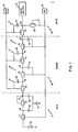
- Fig. 1 shows a schematic layout of a bucket brigade array together with its input and output circuits.
- the array shown is particularly useful as an optical sensor.
- Charge transfer arrays are, at the present time, formed in a single chip of semiconductor material using well known integrated circuit techniques. Because of variations in the semiconductor materials and processes such as resistivity, doping, and photolithography, it was necessary in the past to adjust the input voltage for each and every array circuit so formed.
- the present invention avoids this adjustment problem by introducing a transistor-diode and capacitor circuit at the input of the sensor portion of the array.
- This circuit is self-tracking with all the rest of the elements of the array because it and each of the elements, of the array, are created by exactly the same techniques. In this way, the necessity of individually compensating for each formed array is avoided.
- the invention is best illustrated schematically in Fig. 1.
- the array of the invention comprises a sensor 10, having coupled thereto, an input stage 11 and an output stage 12.
- the sensor 10 comprises a series of storage cells: circuits 13, 14, 15 and 16 arrayed between the input stage 11 and the output stage 12. It should be understood that, for purposes of describing this invention, only four storage cells are shown but that many cells can be used.
- Each storage cell circuit comprises an FET transistor 23, 24, 25 and 26 and a respective capacitor C3, C4, C5 and C6.
- the capacitor of each cell is connected between the gate of its respective transistor and its drain.
- Each transistor in the array is serially connected to the next adjacent transistor.
- the input stage 11 is connected to the source of transistor 23.
- the drain of transistor 23 is connected to the source of transistor 24 and through capacitor C3 to its own gate and to a source of voltage pulses 29.
- the drain of transistor 24 is connected to the source of transistor 25 and through capacitor C4 to its own gate and to a source of voltage pulses 19.
- the drain of transistor 25 is connected to the source of transistor 26 and through capacitor C5 to its own gate and to source 29.
- the drain of transistor 26 is connected to the output and through capacitor C6 to its own gate and source 19.
- the input stage 11 comprises a supply, shown as a 3 V battery 18, coupled to the source of input transistor 21 whose gate is connected to source 19.
- the drain of transistor 21 is coupled through a capacitor Cl to a substrate voltage source Vs.
- This substrate voltage source Vs can be ground, i.e. 0 V or can be any desired voltage in accordance with well known principles of electrical design used in such integrated circuits. For convenience of-description it will herein be presumed that the source Vs is at ground, i.e. 0 V.
- the drain of transistor 21 is also coupled directly to the source of a transistor-diode 22 positioned between input transistor 21 and the first storage cell 13 of the array 10.
- the gate of the transistor 22 is directly connected to its drain thus forming a diode.
- the drain of transistor 22 is connected to the substrate voltage source Vs, through capacitor C2, and directly connected to the source of transistor 23 in the first storage cell 13.
- capacitors Cl and C2 need riot be equal in size and indeed capacitor C2 can be many times larger than the capacitor Cl which, in an integrated circuit, can be the gate-to-source and source-to-substrate parasitic capacitance of transistor 22.
- the output stage 12 includes a transistor-diode 28, a charge amplifier 20 and an output cell 17 which is identical to the storage cells 13, 14, 15 and 16 and is comprised of transistor 27 and capacitor C7. This output cell 17 is coupled between the last cell 16 of the sensor 10 and the charge amplifier 20.
- the source of transistor 27 is connected to the drain of transistor 26 in the last storage cell 16.
- the drain of transistor 27 is connected to its own gate and voltage source 29 through capacitor C7, directly to charge amplifier 20 and to voltage source 19 through the diode connected field effect transistor 28.
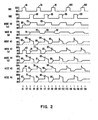
- Fig. 2 illustrates, as a function of time, variations in the voltage pulses applied to the circuits of the invention from the various voltage supplies 19, 29 as well as the voltage pulses taken in the cells at various nodes at different times.
- the described array when built in integrated circuit form is, as discussed above, particularly adapted for use as an optical sensor.
- information is written into the array 10 by exposing the array 10 to light, such that a charge previously stored in the cell array capacitors is caused to be discharged in proportion to the amount of light received by each cell.
- This is a typical operation of such optical sensors.
- the characteristic of charge transfer devices and bucket brigade devices, especially as shown in Fig. 1, is the increasing transfer loss as signal charge decreases for one or a few bits within a long register. Thus, propagation of a "fat zero" bias level reduces the data smearing effect of this transfer loss.
- the circuit shown in Fig. 1 particularly generates a fat zero charge level that is compensated to full charge signal due to process variables.
- the circuit permits a 15% fat zero to be generated regardless of the process variations in such characteristics as threshold voltage, oxide and diffusion capacitance, etc.
- the diode-transistor 22 in the input circuit is especially utilized for generating a background level in the array devices to provide a background level in each of the active array cells 13, 14, 15 and 16, i.e. fat 0's.
- This background level (fat zero) is introduced into the array in the following manner: As shown in Fig. 2 at time tl, a 10 V pulse 61 from the source 19 is applied to the gate of transistors 21, 24, 26 and 28 causing these devices to turn on and become conductive. When transistor 21 turns on, the node 40, which is one plate of capacitor Cl, becomes set at the 3 V level of the voltage source 18 as shown by curve 62. When the 10 V pulse from voltage source 19 is applied to the gate of transistors 24 and 26, capacitor coupling action, through capacitors C4 and C6 respectively, causes nodes 43 and 45 to both rise to 10 V as shown by pulses 63 and 64.
- nodes 42 and 44 rise to the 8 V level as shown by curves 65 and 66.
- Nodes 42 and 44 rise only to the 8 V level because there is approximately a 2 V threshold drop through each of the transistors 24 and 26.
- the application of the pulse 61 to the transistor 28 causes node 46 to also rise to the 8 V level. Because node 41 is isolated by virtue of transistor 23 being off, it remains at 0 V.
- the pulse at 61 terminates, and transistors 21, 24, 26, and 28 are shut off and nodes 43 and 45 return to zero. Because nodes 40, 42, 44 and 46 are now isolated, they remain at the voltage to which they were raised. However, because nodes 43 and 45 were only capacitively coupled to the source 19, they return to 0 V.
- the supply 29 turns on and applies a 10 V pulse 68 to the gates of transistors 23, 25 and 27.
- nodes 42, 44, and 46 rise from 8 V to 18 V as indicated by curves 69, 70 and 71.
- transistors 23, 25, and 27 are turned on, charge transfer through the transistors begins and the nodes 42, 44 and 46 fall.
- the nodes 43 and 45 rise to 8 V which is one threshold voltage below the applied gate voltage pulse 68, as indicated by curves 72 and 73.
- transistor 23 turns on and node 42 rises to 18 V
- the node 41 is coupled through transistor 23 to the node 42 and it tries to rise to 8 V.
- node 41 is coupled through transistor 23 to the entire charge transfer device.
- node 41 immediately becomes coupled to node 40 through transistor diode 22.
- node 41 only rises to about 7 V (instead of 8 V) and the node 40 rises to about 5 V which is once again a threshold below the voltage applied to the gate of the transistor 22.
- This rise in voltage of the node 41 is indicated as pulse 74 and the rise of node 40 is indicated as pulse of 75.
- the pulse terminates and the nodes 42, 44, and 46 all return to zero.
- nodes 40, 41, 43 and 45 all remain at the levels which they have been set.
- node 40 is now reduced down to the 3 V level by the turning on of transistor 21 and node 41 is reduced from 7 V to a 5 V level which is a threshold above the level to which node 40 has been reduced. This is shown by the decrease in slope of curve 82.
- the voltage change on nodes 40 and 41 generate the fat zero level to be propagated into the charge transfer array.
- source 19 supplies a 10 V pulse 91 which causes node 40 to return to the 3 V level and node 41 to decline to the 5 V level as indicated by pulse 92. Simultaneously nodes 43 and 45 go to 18 V indicated by pulses 93 and 94 respectively which in turn causes nodes 42, 44 and 46 to rise to 8 V as shown by pulses 95, 96, and 97 respectfully.
- pulse 91 is terminated and node 43 declines to the 2 V level while node 45 returns to zero.
- both nodes 42 and 43, i.e., cells 13 and 14 have a 2 V level introduced into them.
- the 2 V fat zero level is transferred into the entire array by the sequential applications of additional pulses from sources 29 and 19.
- the additional pulses 99, 100, 101 and 102 cause the fat zero to be propagated down the entire array.
- the node 44 does not return to zero but instead is left at the fat zero level of 2 V.
- node 45 is left at the fat zero level, while node 46 receives the fat zero level at time tl6 upon termination of pulse 101.
- t16 a fat zero has been propagated down the entire array to the charge amplifier and each array cell 13, 14, 15 and 16 now has a fat zero introduced into it.
- the described array when built as an integrated circuit, is particularly adapted for use as an optical sense array, information may be written into the array by exposing the array to light so that a charge is stored in each array cell which is not shielded; i.e. cells 13 and 15 can be caused to be charged in proportion to the amount of light received by each cell.
- each of the storage cells 13, 14, 15 and 16 have had their respective capacitors C3, C4, C5 and C6 set to "fat zero" so that if one or more cells receive no light, the transfer efficiency is improved for those cells with a light signal.
- the array can now be utilized as, a scanner or the like, as is well known to the charge transfer, i.e., charge coupled or bucket brigade technology.
Landscapes
- Engineering & Computer Science (AREA)
- Microelectronics & Electronic Packaging (AREA)
- Power Engineering (AREA)
- Solid State Image Pick-Up Elements (AREA)
- Transforming Light Signals Into Electric Signals (AREA)
- Networks Using Active Elements (AREA)
Applications Claiming Priority (2)
| Application Number | Priority Date | Filing Date | Title |
|---|---|---|---|
| US06/202,107 US4358831A (en) | 1980-10-30 | 1980-10-30 | Self-biasing circuit for analog shift registers, with fat zero compensation |
| US202107 | 1980-10-30 |
Publications (2)
| Publication Number | Publication Date |
|---|---|
| EP0051115A2 true EP0051115A2 (fr) | 1982-05-12 |
| EP0051115A3 EP0051115A3 (fr) | 1983-07-06 |
Family
ID=22748527
Family Applications (1)
| Application Number | Title | Priority Date | Filing Date |
|---|---|---|---|
| EP81106256A Withdrawn EP0051115A3 (fr) | 1980-10-30 | 1981-08-11 | Circuit générateur d'autopolarisation pour appareils à transfert de charges et systèmes de mémoire utilisant ce circuit |
Country Status (3)
| Country | Link |
|---|---|
| US (1) | US4358831A (fr) |
| EP (1) | EP0051115A3 (fr) |
| JP (1) | JPS59918B2 (fr) |
Cited By (1)
| Publication number | Priority date | Publication date | Assignee | Title |
|---|---|---|---|---|
| WO2020109668A1 (fr) * | 2018-11-29 | 2020-06-04 | Oy Ajat Ltd. | Circuit de détecteur |
Families Citing this family (2)
| Publication number | Priority date | Publication date | Assignee | Title |
|---|---|---|---|---|
| IT1225949B (it) | 1988-07-11 | 1990-12-10 | Fiat Auto Spa | Sospensione per ruote anteriori sterzanti di un autoveicolo |
| JPH08114491A (ja) * | 1994-02-15 | 1996-05-07 | Nippon Dainamatsuto Kk | はかりマット |
Family Cites Families (5)
| Publication number | Priority date | Publication date | Assignee | Title |
|---|---|---|---|---|
| US3801826A (en) * | 1972-05-12 | 1974-04-02 | Teletype Corp | Input for shift registers |
| US3911290A (en) * | 1974-06-10 | 1975-10-07 | Ibm | N-phase bucket brigade optical scanner |
| US4010485A (en) * | 1974-06-13 | 1977-03-01 | Rca Corporation | Charge-coupled device input circuits |
| JPS592998B2 (ja) * | 1975-12-29 | 1984-01-21 | 松下電器産業株式会社 | デンカテンソウソウチ |
| DE2842856C3 (de) * | 1978-10-02 | 1981-09-03 | Siemens AG, 1000 Berlin und 8000 München | Ladungsverschiebespeicher in Seriell-Parallel-Seriell-Organisation mit vollständigem Grundladungsbetrieb |
-
1980
- 1980-10-30 US US06/202,107 patent/US4358831A/en not_active Expired - Lifetime
-
1981
- 1981-08-11 EP EP81106256A patent/EP0051115A3/fr not_active Withdrawn
- 1981-09-03 JP JP56137885A patent/JPS59918B2/ja not_active Expired
Cited By (5)
| Publication number | Priority date | Publication date | Assignee | Title |
|---|---|---|---|---|
| WO2020109668A1 (fr) * | 2018-11-29 | 2020-06-04 | Oy Ajat Ltd. | Circuit de détecteur |
| CN113614576A (zh) * | 2018-11-29 | 2021-11-05 | Oy直接转换有限公司 | 检测器电路 |
| US11921244B2 (en) | 2018-11-29 | 2024-03-05 | Oy Direct Conversion Ltd. | Detector circuit |
| CN113614576B (zh) * | 2018-11-29 | 2024-09-06 | Oy直接转换有限公司 | 检测器电路 |
| US12436303B2 (en) | 2018-11-29 | 2025-10-07 | Oy Varex Imaging Finland Ltd. | Detector circuit |
Also Published As
| Publication number | Publication date |
|---|---|
| JPS59918B2 (ja) | 1984-01-09 |
| EP0051115A3 (fr) | 1983-07-06 |
| JPS5778700A (en) | 1982-05-17 |
| US4358831A (en) | 1982-11-09 |
Similar Documents
| Publication | Publication Date | Title |
|---|---|---|
| EP0144637B1 (fr) | Système de génération de tension pour une mémoire R.A.M. non-volatile | |
| US4670668A (en) | Substrate bias generator with power supply control means to sequence application of bias and power to prevent CMOS SCR latch-up | |
| JP2528196B2 (ja) | 電圧逓倍回路 | |
| EP1237266B1 (fr) | Circuit élévateur de tension à sémi-conducteur | |
| EP0394705B1 (fr) | Système de mémoire non volatile pour mémorisation de valeur multiple | |
| US3996482A (en) | One shot multivibrator circuit | |
| US4039861A (en) | Cross-coupled charge transfer sense amplifier circuits | |
| US4920280A (en) | Back bias generator | |
| EP0098417A2 (fr) | Dispositif de mémoire semi-conductrice | |
| US4845670A (en) | Memory device using shift-register | |
| US3955101A (en) | Dynamic reference voltage generator | |
| US5394027A (en) | High voltage charge pump and related circuitry | |
| US4384216A (en) | Controlled power performance driver circuit | |
| JPS6122397B2 (fr) | ||
| US4384218A (en) | Substrate bias generator | |
| EP0030130B1 (fr) | Oscillateur et EPROM comportant un tel oscillateur | |
| US4455493A (en) | Substrate bias pump | |
| EP0168246A2 (fr) | Circuit actif de tirage | |
| US4358831A (en) | Self-biasing circuit for analog shift registers, with fat zero compensation | |
| EP0481531B1 (fr) | Dispositif de transfert de charge | |
| GB2072419A (en) | Mos integrated circuit device | |
| US3648065A (en) | Storage circuit for shift register | |
| US4468576A (en) | Inverter circuit having transistors operable in a shallow saturation region for avoiding fluctuation of electrical characteristics | |
| US4494015A (en) | Pulse enhancement circuit for digital integrated circuit | |
| EP0170781A2 (fr) | Dispositif de mémoire MOS dynamique |
Legal Events
| Date | Code | Title | Description |
|---|---|---|---|
| PUAI | Public reference made under article 153(3) epc to a published international application that has entered the european phase |
Free format text: ORIGINAL CODE: 0009012 |
|
| 17P | Request for examination filed |
Effective date: 19810811 |
|
| AK | Designated contracting states |
Designated state(s): DE FR GB |
|
| PUAL | Search report despatched |
Free format text: ORIGINAL CODE: 0009013 |
|
| AK | Designated contracting states |
Designated state(s): DE FR GB |
|
| STAA | Information on the status of an ep patent application or granted ep patent |
Free format text: STATUS: THE APPLICATION IS DEEMED TO BE WITHDRAWN |
|
| 18D | Application deemed to be withdrawn |
Effective date: 19840412 |
|
| RIN1 | Information on inventor provided before grant (corrected) |
Inventor name: TOMPKINS, JAMES DARRELL |