EP0051473B1 - Phasenriegelschleife mit einer Schleife zur Anfangssynchronisierung - Google Patents
Phasenriegelschleife mit einer Schleife zur Anfangssynchronisierung Download PDFInfo
- Publication number
- EP0051473B1 EP0051473B1 EP81305174A EP81305174A EP0051473B1 EP 0051473 B1 EP0051473 B1 EP 0051473B1 EP 81305174 A EP81305174 A EP 81305174A EP 81305174 A EP81305174 A EP 81305174A EP 0051473 B1 EP0051473 B1 EP 0051473B1
- Authority
- EP
- European Patent Office
- Prior art keywords
- signal
- phase
- output signal
- frequency
- responsive
- Prior art date
- Legal status (The legal status is an assumption and is not a legal conclusion. Google has not performed a legal analysis and makes no representation as to the accuracy of the status listed.)
- Expired
Links
Images

Classifications
-
- H—ELECTRICITY
- H03—ELECTRONIC CIRCUITRY
- H03L—AUTOMATIC CONTROL, STARTING, SYNCHRONISATION OR STABILISATION OF GENERATORS OF ELECTRONIC OSCILLATIONS OR PULSES
- H03L7/00—Automatic control of frequency or phase; Synchronisation
- H03L7/06—Automatic control of frequency or phase; Synchronisation using a reference signal applied to a frequency- or phase-locked loop
- H03L7/08—Details of the phase-locked loop
- H03L7/10—Details of the phase-locked loop for assuring initial synchronisation or for broadening the capture range
- H03L7/113—Details of the phase-locked loop for assuring initial synchronisation or for broadening the capture range using frequency discriminator
-
- H—ELECTRICITY
- H04—ELECTRIC COMMUNICATION TECHNIQUE
- H04L—TRANSMISSION OF DIGITAL INFORMATION, e.g. TELEGRAPHIC COMMUNICATION
- H04L27/00—Modulated-carrier systems
- H04L27/02—Amplitude-modulated carrier systems, e.g. using on-off keying; Single sideband or vestigial sideband modulation
- H04L27/06—Demodulator circuits; Receiver circuits
- H04L27/066—Carrier recovery circuits
Definitions
- This invention is related generally to phase-locked loops and specifically to phase-locked loops having components for assuring initial lock to an incoming signal.
- phase-locked loop hereinafter PLL.
- a PLL is typically comprised of a phase detector, a low-pass filter, an amplifier, and a voltage controlled oscillator, hereinafter VCO.
- the phase detector compares the phase of an input signal to the phase of a variable frequency output signal which is produced by the VCO.
- the phase detector produces an output voltage that is representative of the instantaneous difference between the input signal and the output signal.
- the output voltage of the phase detector is filtered, amplified and input to the VCO.
- the frequency of the output signal produced by the VCO varies with the voltage input thereto, which voltage is representative of the phase difference between the input signal and the output signal. In this manner the phase and frequency of the output signal is locked to the phase and frequency of the input signal.
- the bandwidth chosen must be a compromise between competing design criteria. It is desirable to have a wide bandwidth thus allowing for initial synchronization, or capture, over a wide range of frequencies. However, a wide bandwidth will have poor noise rejection characteristics and thus the output signal may not precisely track the input signal. In order to increase the precision with which the output signal tracks the input signal it is necessary to decrease the bandwidth. This decrease in bandwidth will, however, reduce the capture range of the PLL. Thus, the bandwidth chosen for the typical PLL must be a compromise between a wide bandwidth allowing for fast acquisition over a wide range of frequencies and a narrow bandwidth allowing for noise-free tracking of the input signal.
- One prior art technique for avoiding this compromise is to have two loops responsive to the received signal such as in US-A-3 909 735.
- One loop has a large bandwidth for fast acquisition over a wide range of frequencies; the second loop has a narrow bandwidth for error-free tracking.
- a switch responsive to the difference between the input signal and the output signal, determines which loop is connected to the VCO. When the difference is large, the loop having the large bandwidth is connected to the VCO. Conversely, when the difference is small, the loop having the narrow bandwidth is connected to the VCO.
- the chief object of the present invention is to provide a phase-locked circuit loop which overcomes the problems of the prior art.
- the invention resides in a phase-locked circuit loop producing an output signal having a frequency locked to the frequency of an input signal, comprising: means for producing the output signal, said output signal having a variable frequency; first means for detecting a phase difference betwaen said input signal and said output signal, said first phase detection means having a narrow bandwidth; means for producing a reference signal independent of the output signal of said means for producing the output signal; second means for detecting a phase difference between said reference signal and said output signal, said second phase detection means having a wide bandwidth; control means responsive to said second phase detection means, said control means producing a switching signal representative of the frequency difference between said independent reference signal and said output signal; and switching means selectively connecting one of said first phase detection means and said second phase detection means to said means producing said output signal, said switching means being responsive to said switching signal such that when said frequency difference between said independent reference signal and said output signal is large said second phase detection means is connected to said means producing said output signal.
- the present disclosure reveals a phase-locked circuit loop having an initialization loop for initially pulling the frequency of an output signal very close to the frequency of an input signal such that locking is assured.
- An integrator and a voltage controlled oscillator produce the variable frequency output signal and are common components to both a first and a second loop.
- the first, or primary, loop has a narrow bandwidth and is locked to the input signal.
- the first loop compares the input signal to the variable frequency output signal.
- a second, or initialization, loop has a wide bandwidth and is locked to the reference signal.
- the second loop compares the reference signal to the variable frequency output signal.
- the reference signal has a frequency approximately equal to the frequency of the input signal.
- An off-frequency detector is responsive to the comparison of the reference signal to the output signal and produces a switching control signal representative of this comparison.
- a switch selectively connects the remainder of the components of one of the first loop and the second loop to the integrator and the voltage controlled oscillator.
- the switch is responsive to the switching control signal such that the components of the first loop are connected to the integrator and the voltage controlled oscillator when the difference between the reference signal and the output signal is small and the components of the second loop are connected to the integrator and the voltage controlled oscillator when the difference between the reference signal and the output signal is large.
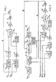
- FIG. 1 illustrates a block diagram of a simplified phase-locked loop 10 having an initialization loop for assuring locking.
- the phase-locked loop 10 produces a variable frequency output signal V out which is locked in phase and frequency to an input signal V ln'
- the output signal V Out is produced by a voltage controlled oscillator (VCO) 12.
- VCO voltage controlled oscillator
- the frequency of the output signal V Out is determined by the magnitude of the voltage input to the VCO 12.
- the output signal V Out is fed back to a first phase detector 14.
- the first phase detector 14 compares the phase of the output signal V Out to the phase of the input signal V ln'
- a filter 15 is responsive to the first phase detector 14.
- the output signal V Out is also fed back to a second phase detector 17.
- the second phase detector 17 compares the phase of the output signal V Out to the phase of an internally generated reference signal V Ref .
- the reference signal V Ref has a frequency approximately equal to the frequency of the input signal V ln'
- An amplifier 18, having a large bandwidth, is responsive to the second phase detector 17.
- An off-frequency detector 20 is responsive to the amplifier 18.
- the off-frequency detector 20 produces a switching control signal V sw which is responsive to the frequency difference between the frequency of the output signal V Out and the frequency of the reference signal V Ref .
- a switch 22 selectively connects both the filter 15 and the amplifier 18 to an integrator 23.
- the switch 22 is responsive to the switching control signal V sw such that the filter 15 is connected to the integrator 23 when the frequency difference between the output signal V out and the reference signal V Rel is small and the amplifier 18 is connected to the integrator 23 when the frequency difference between the output signal and the reference signal is large.
- the integrator 23 produces a control voltage which is input to the VCO 12.
- the second phase detector 17, the amplifier 18 and the integrator 23 are used to pull the output signal V Out within a given range of the reference signal V Ref as determined by the off-frequency detector 20; the first phase detector 14, the filter 15, and the integrator 23 allow the output signal V Out to precisely track the input signal V ln' after the output signal has been pulled within the range determined by the off-frequency detector 20.
- FIG. 2 a block diagram of a single sideband receiver circuit 25 utilizing a phase-locked loop constructed according to the teachings of the present invention for the recovery of an informational signal from a received signal V Rec is shown. It is to be understood that the present invention is not limited to this particular application. Where appropriate, identical components performing identical functions will have the same reference numeral as assigned in Figure 1.
- the received signal V Rec is input to an input filter 27.
- the received signal VRec is typically composed of a data signal V D occupying a discrete frequency spectrum and a pilot tone Vp having a frequency adjacent to the frequency spectrum of the data signal.
- the filtered, received signal V Rec is input to a signal processing circuit 29.
- the signal processing circuit 29 may be of a type described in U.S. Patent Application Serial No. 202,553 filed October 31,1980 (W. E. Case No. 49,025) wherein the frequencies of the data signal V D and the pilot tone Vp are translated to predetermined intermediate frequencies.
- the intermediate frequency pilot tone is then separated by filters from the intermediate frequency data signal.
- the frequency of the intermediate frequency pilot tone is translated to a frequency sufficiently removed from the frequency spectrum of the intermediate frequency data signal so as not to interfere therewith.
- Both the intermediate frequency data signal and the translated, intermediate frequency, pilot tone are amplified in an automatic gain controlled amplifier.
- the output signal of the amplifier corresponds to the output signal of the signal processing circuit 29 shown in Figure 2.
- the output signal of the signal processing circuit 29 is input to a demodulator 30.
- the demodulator 30 also receives a regenerated pilot tone Vp'.
- the demodulator produces an output signal V out which is composed of both an audio output signal V Aud corresponding to the received data signal V D and a recovered pilot tone corresponding to the received pilot tone Vp.
- the output signal V Out is input to an output filter 31 which passes the audio output signal V Aud thus conveying the desird information to the user.
- the output signal V out of the demodulator 30 is input to both the signal processing circuit 29 (for automatic gain control) and a first mixer, or phase detector, 35 through a selective amplifier 33.
- the selective amplifier 33 acts as a filter as well as a buffer.
- the first mixer 35 additionally receives a first reference signal VRfl.
- An output signal of the first mixer 35 represents the phase difference between the recovered pilot tone and the reference signal V Ref1 .
- This output signal is input to the filter 15.
- the filter 15 is selectively connected to the integrator 23 by the switch 22.
- the integrator 23 produces the control voltage which is input to the voltage controlled oscillator 12.
- the voltage controlled oscillator 12 produces the regenerated pilot tone Vp' which is input to the demodulator 30.
- the regenerated pilot tone Vp' is additionally input to a second mixer, or phase detector, 36.
- the second mixer 36 also receives a second reference signal V REF2 .
- An output signal of the second mixer 36 is input to a third mixer, or phase detector, 37.
- a third reference signal V Ref3 is input to the third mixer 37.
- An output signal of the third mixer 37 is amplified by the amplifier 18.
- the amplifier 18 is selectively connected by the switch 22 to the integrator 23.
- the off-frequency detector 20 is responsive to the amplifier 18 and produces the switching control signal V sw which controls the operation of the switch 22.
- the demodulator 30, the first mixer 35, the filter 15, the switch 22, the integrator 23, and the oscillator 12 form a loop 39 which acts as both a translation loop and a pilot regeneration loop.
- the second mixer 36, the third mixer 37, the amplifier 18, the switch 22, the integrator 23, and the oscillator 12 form an initialization loop 41.
- both the intermediate frequency pilot tone and the translated, intermediate frequency, pilot tone have predetermined frequencies.
- the pilot tone has a frequency of 5.2 megahertz and the translated, intermediate frequency, pilot tone has a frequency of 4.783 megahertz.
- the initialization loop 41 is therefore necessary to pull the voltage controlled oscillator 12 within the locking range of the translation and regeneration loop 39;
- the frequency of the regenerated pilot tone Vp' may be compared by the initialization loop 41 to a reference signal having a frequency approximately that of the known frequency of the translated, intermediate frequency, pilot tone. Because an internally generated reference signal is used by the initialization loop 41 to pull the oscillator 12 within the locking range of the translation and regeneration loop 39 initial locking will occur quickly no matter what the frequency of the regenerated pilot tone Vp' is initially.
- the regenerated pilot tone Vp' is compared by the second mixer 36 to the second reference signal V Ref2 which has a frequency of five megahertz.
- the resulting signal is compared by the third mixer 37 to the third reference signal V Ref3 having a frequency of 0.2 megahertz. If the regenerated pilot tone Vp' has a frequency of 5.2 megahertz the resulting output signal of the third mixer 37 will have a frequency of zero.
- the off-frequency detector 20 will determine that the frequency of the regenerated pilot tone Vp' is within the capture range of the translation and regeneration loop 41.
- the off-frequency detector 20 will cause the switch 22 to connect the filter 15 to the integrator 23.
- the off-frequency detector 20 may be adjusted by the user to determine a "window of acceptability" for the frequency of the regenerated pilot tone Vp'. A typical window of acceptability would allow the frequency of the regenerated pilot tone Vp' to vary by fourteen hertz above or below the 5.2 megahertz value.
- the recovered pilot tone when the regenerated pilot tone Vp' is within the window of acceptability, the recovered pilot tone, which is a portion of the output signal V Out , will have a frequency of 417 kilohertz ⁇ 14 herts depending upon the exact frequency of the regenerated pilot tone Vp'.
- the recovered pilot tone is compared by the first mixer 35 to the first reference signal VRef1 which has a frequency of 417 kilohertz.
- the resulting output signal of the first mixer 35 is representative of the tracking error between the regenerated pilot tone Vp' and the translated, intermediate frequency, pilot tone.
- the output signal of the first mixer 35 is filtered and integrated by the filter 15 and the integrator 23, respectively, before being input to the voltage controlled oscillator 12.
- the off-frequency detector 20 is considered to be an important feature of the present invention and is shown in block diagram form in Figure 3.
- a Schmitt trigger 44 is responsive to the output signal of the amplifier 18 which is shown in Figure 3 as a sine wave 51.
- a one-shot multivibrator 45 is responsive to the output signal of the Schmitt trigger 44 which is shown as a square wave 52.
- the one-shot multivibrator 45 is connected to a positive voltage source through an adjustable resistor 46.
- a D-type flip-flop 47 has a set terminal S, a D input terminal responsive to the one-shot 45, a clock C1 input terminal responsive to the Schmitt trigger 44, a reset terminal R connected to the one-shot 45 through an inverter 48, a Q output terminal, and a Q output terminal.
- the Q output terminal of the flip-flop 47 produces the switching signal V sw which is input to a second one-shot multivibrator 49.
- An output signal of the second one-shot multivibrator 49 is also
- the Schmitt trigger 44 is responsive to the sine wave 51.
- the sine wave 51 is produced by the second phase detector 17 shown in Figure 1 and has a frequency representative of the difference between the frequency of the output signal V out and the frequency of the reference signal V Ref .
- the Schmitt trigger 44 produces the square wave 52 which has a frequency responsive to the frequency of the sine wave 51.
- the square wave 52 is input to the one-shot multivibrator 45.
- a one-shot is a circuit which produces an output signal of fixed duration when an input signal of any duration is applied.
- the time period of the square wave 52 is compared to the time period of an output signal of the one-shot 45. If the time period of the square wave 52 is shorter than the time period of the output signal of the one-shot 45, output signal will remain in a high state. Conversely, if the time period of the square wave 52 is longer than the time period of the output signal of the one-shot 45, the output signal will vary from a high to a low state.
- the time period of the output signal of the one-shot 45 may be varied by adjusting the resistance value of the adjustable resistor 46.
- the value of the resistor 46 determines the window of acceptability for the off-frequency detector 20. Increasing the value of the resistor 46 decreases the window of acceptability. Conversely, decreasing the value of the resistor 46 increases the window of acceptability.
- the flip-flop 47 will clock the high state of the output signal from the one-shot 45 from the D input terminal to the Q output terminal on each positive going transition from the Schmitt trigger 44. This results in the switching control signal V sw being available at the Q output terminal.
- the inverter 48 between the one-shot 45 and the reset terminal R of the flip-flop 47 eliminates hangup of the off-frequency detector 20 in the situation where the frequency of the sine wave 51 is high, and immediately goes to zero, as might happen if the initialization loop locks very quickly. If the initialization loop locks very quickly the output signal of the one-shot 45 goes low and the flip-flop 47 must be reset since there are no positive going transitions in the square wave 52 to clock the flip-flop 47.
- the second one-shot 49 delays the switching control signal V sw thus insuring that the initialization loop is given sufficient time to completely lock to the reference signal V Ref .
- the circuit details of the off-frequency detector 20 are shown in Figure 4.
- the circuit shown in Fig. 4 uses positive logic and a positive ground, i.e., ground potential is a logic one.
- the sine wave 51 is input to a set terminal S of a flip-flop 54 through a resistor 55.
- a D input terminal, a clock input terminal C1, a reset terminal R are all connected to ground.
- the set terminal S of the flip-flop 54 is connected to a first input terminal of a first NAND gate 57 through the series combination of a resistor 58 and a capacitor 59.
- the junction between the resistor 58 and the capacitor 59 is connected to a Q output terminal of the flip-flop 54.
- the square wave 52 is available at the Q output terminal.
- the flip-flop 54 and associated resistors provide the function of the Schmitt trigger 44 shown in Figure 3.
- the first input terminal of the NAND gate 57 is connected to a negative voltage source through the parallel combination of a diode 61 and a resistor 62.
- a second input terminal of the NAND gate 57 is connected to ground.
- An output terminal of the NAND gate 57 is connected to a base terminal of a transistor 64 through a resistor 65.
- An emitter terminal of the transistor 64 is connected to ground through a diode 66.
- a collector terminal of the transistor 64 is connected to a negative voltage source through the series combination of the adjustable resistor 46 and a resistor 67.
- the junction between the resistor 46 and the resistor 67 is connected to ground through a capacitor 68 and is connected to a first input terminal of a second NAND gate 70.
- a second input terminal of the NAND gate 70 is connected to ground.
- An output terminal of the NAND gate 70 is connected to both a first input terminal of a third NAND gate 71 and the reset terminal R of the flip-flop 47.
- a second input terminal of the third NAND gate 71 is connected to ground.
- An output terminal of the third NAND gate 71 is connected to the D input terminal of the flip-flop 47.
- the clock input terminal C1 of the flip-flop 47 is connected to the Q output terminal of the flip-flop 54.
- the set terminal S of the flip-flop 47 is connected to a negative voltage source through a resistor 73.
- the set terminal S of the flip-flop 47 is also connected to the Q output terminal thereof, through a capacitor 74.
- the switching signal V sw is available at the Q output terminal of the flip-flop 47.
- the capacitor 74 provides an AC coupled, positive feedback voltage to the set terminal S of the flip-flop 47.
- the capacitor causes the signal input to the set terminal S to remain high until the capacitor 74 has discharged. This causes the switching signal V sw to remain high for a fixed duration.
- the combination of the flip-flop 47 and the capacitor 74 provide the function of the one-shot 49 shown in Figure 3.
- the IT output terminal of the flip-flop 47 is connected to a base terminal of a transistor 76 through a resistor 77.
- An emitter terminal of the transistor 76 is connected to ground through a diode 78.
- a collector terminal of the transistor 76 is connected to a negative voltage source through the series combination of a resistor 79 and a resistor 80.
- An off-frequency alarm signal V A is available at the junction between the resistors 79 and 80.
- the off-frequency alarm signal V A is delayed by the transistor 76 such that an off-frequency condition must exist for a predetermined period of time prior to the production of the off-frequency alarm signal V " .
- the signal V A may be used to provide an appropriate audio or visual alarm.
- a phase-locked loop having a first loop locked to an incoming signal and a second loop locked to an internally generated reference signal.
- the first loop has a narrow bandwidth for error-free tracking of the input signal while the second loop has a wide bandwidth to assure initial locking.
- An off-frequency detector and a switch determine whether the first or second loop is engaged.
Landscapes
- Engineering & Computer Science (AREA)
- Computer Networks & Wireless Communication (AREA)
- Signal Processing (AREA)
- Stabilization Of Oscillater, Synchronisation, Frequency Synthesizers (AREA)
Claims (14)
Applications Claiming Priority (2)
| Application Number | Priority Date | Filing Date | Title |
|---|---|---|---|
| US06/202,554 US4365211A (en) | 1980-10-31 | 1980-10-31 | Phase-locked loop with initialization loop |
| US202554 | 1980-10-31 |
Publications (2)
| Publication Number | Publication Date |
|---|---|
| EP0051473A1 EP0051473A1 (de) | 1982-05-12 |
| EP0051473B1 true EP0051473B1 (de) | 1985-06-19 |
Family
ID=22750359
Family Applications (1)
| Application Number | Title | Priority Date | Filing Date |
|---|---|---|---|
| EP81305174A Expired EP0051473B1 (de) | 1980-10-31 | 1981-10-30 | Phasenriegelschleife mit einer Schleife zur Anfangssynchronisierung |
Country Status (8)
| Country | Link |
|---|---|
| US (1) | US4365211A (de) |
| EP (1) | EP0051473B1 (de) |
| JP (1) | JPS57106241A (de) |
| BR (1) | BR8107034A (de) |
| DE (1) | DE3171060D1 (de) |
| ES (1) | ES506676A0 (de) |
| MX (1) | MX152567A (de) |
| ZA (1) | ZA817156B (de) |
Families Citing this family (41)
| Publication number | Priority date | Publication date | Assignee | Title |
|---|---|---|---|---|
| JPS5850827A (ja) * | 1981-09-08 | 1983-03-25 | Fujitsu Ltd | フェーズ・ロック・ループ回路 |
| US4484152A (en) * | 1982-05-19 | 1984-11-20 | Westinghouse Electric Corp. | Phase-locked loop having improved locking capabilities |
| JPS6014522A (ja) * | 1983-07-06 | 1985-01-25 | Mitsubishi Electric Corp | デジタル信号に同期したクロツク信号発生装置 |
| GB2143385A (en) * | 1983-07-13 | 1985-02-06 | Plessey Co Plc | Phase lock loop circuit |
| US4583060A (en) * | 1983-08-22 | 1986-04-15 | Rca Corporation | High speed voltage tunable frequency filter or frequency generator |
| US4580107A (en) * | 1984-06-06 | 1986-04-01 | The United States Of America As Represented By The Secretary Of The Air Force | Phase lock acquisition system having FLL for coarse tuning and PLL for fine tuning |
| FR2573592B1 (fr) * | 1984-11-20 | 1993-12-10 | Bull Sa | Circuit oscillateur asservi en phase a un signal de frequence predeterminee |
| US4593254A (en) * | 1984-12-14 | 1986-06-03 | International Business Machines Corp. | VCO centering circuit |
| JPS61150525A (ja) * | 1984-12-25 | 1986-07-09 | Nec Corp | 位相同期回路 |
| US4829545A (en) * | 1986-08-25 | 1989-05-09 | Guzik Technical Enterprises, Inc. | Method and apparatus for data window centering ina multifrequency data separator |
| US4835481A (en) * | 1986-09-30 | 1989-05-30 | Siemens Aktiengesellschaft | Circuit arrangement for generating a clock signal which is synchronous in respect of frequency to a reference frequency |
| US4787097A (en) * | 1987-02-11 | 1988-11-22 | International Business Machines Corporation | NRZ phase-locked loop circuit with associated monitor and recovery circuitry |
| US4806879A (en) * | 1987-05-01 | 1989-02-21 | Ecrm Incorporated | Method and apparatus for synchronizing to a pulse train packet signal |
| JP2520697B2 (ja) * | 1987-10-23 | 1996-07-31 | アンリツ株式会社 | 位相信号濾波装置 |
| IT1223524B (it) * | 1987-12-18 | 1990-09-19 | Honeywell Bull Spa | Circuito ad aggancio di fase autotarante |
| GB2223136B (en) * | 1988-03-28 | 1992-10-14 | Plessey Co Plc | Broad band vco control system for clock recovery |
| DE3816696A1 (de) * | 1988-05-17 | 1989-11-30 | Philips Patentverwaltung | Schaltungsanordnung zum synchronisieren eines in der frequenz steuerbaren oszillators |
| US4882549A (en) * | 1988-11-16 | 1989-11-21 | Zvi Galani | Center offset microwave frequency synthesizer |
| US4885553A (en) * | 1988-11-30 | 1989-12-05 | Motorola, Inc. | Continuously adaptive phase locked loop synthesizer |
| FR2651937B1 (fr) * | 1989-09-14 | 1994-04-08 | Alcatel Espace | Transpondeur de mise a poste d'un satellite. |
| FR2661752B1 (fr) * | 1990-05-07 | 1992-07-10 | Dassault Electronique | Recepteur d'un signal electromagnetique de frequence nominale connue susceptible d'etre affecte d'une variation inconnue, notamment par decalage doppler. |
| US5223755A (en) * | 1990-12-26 | 1993-06-29 | Xerox Corporation | Extended frequency range variable delay locked loop for clock synchronization |
| DE4125995A1 (de) * | 1991-06-08 | 1992-12-10 | Licentia Gmbh | Empfaengeranordnung |
| US5142246A (en) * | 1991-06-19 | 1992-08-25 | Telefonaktiebolaget L M Ericsson | Multi-loop controlled VCO |
| JP3137370B2 (ja) * | 1991-08-07 | 2001-02-19 | 株式会社東芝 | デジタルpll回路 |
| JP3208736B2 (ja) * | 1991-11-08 | 2001-09-17 | ソニー株式会社 | Pll回路 |
| JP3033654B2 (ja) * | 1993-08-23 | 2000-04-17 | 日本電気株式会社 | Pll周波数シンセサイザ |
| GB9320069D0 (en) * | 1993-09-29 | 1993-11-17 | Sgs Thomson Microelectronics | Frequency tuning for a phase locked loop |
| US5512860A (en) * | 1994-12-02 | 1996-04-30 | Pmc-Sierra, Inc. | Clock recovery phase locked loop control using clock difference detection and forced low frequency startup |
| JPH08213901A (ja) * | 1995-02-02 | 1996-08-20 | Fujitsu Ltd | 位相同期回路及びこれを構成するための回路装置並びに位相同期回路を用いた電子装置 |
| IT1279165B1 (it) * | 1995-03-14 | 1997-12-04 | Cselt Centro Studi Lab Telecom | Circuito per l'estrazione del segnale di orologio da un flusso dati ad alta velocita'. |
| WO1997007594A1 (fr) * | 1995-08-14 | 1997-02-27 | Hitachi, Ltd. | Circuit de verrouillage de phase et dispositif de reproduction d'image |
| US5666084A (en) * | 1995-12-01 | 1997-09-09 | Motorola, Inc. | Multi-level demodulator and VCO circuit |
| US5856753A (en) * | 1996-03-29 | 1999-01-05 | Cypress Semiconductor Corp. | Output circuit for 3V/5V clock chip duty cycle adjustments |
| US5802450A (en) * | 1996-04-19 | 1998-09-01 | Ericsson Inc. | Transmit sequencing |
| US5838205A (en) * | 1997-02-18 | 1998-11-17 | International Business Machines Corporation | Variable-speed phase-locked loop system with on-the-fly switching and method therefor |
| US20030039013A1 (en) * | 2001-08-27 | 2003-02-27 | Jones David J. | Dynamic dispersion compensation in high-speed optical transmission systems |
| US6617932B2 (en) * | 2001-08-27 | 2003-09-09 | Axe, Inc. | System and method for wide dynamic range clock recovery |
| US7317778B2 (en) * | 2003-01-31 | 2008-01-08 | Hewlett-Packard Development Company, L.P. | Phase-locked loop control circuit |
| US20080158076A1 (en) * | 2006-12-28 | 2008-07-03 | Broadcom Corporation | Dynamically adjustable narrow bandwidth antenna for wide band systems |
| CN109121058B (zh) * | 2018-07-06 | 2020-11-06 | 江西洪都航空工业集团有限责任公司 | 一种音频信号的测试方法 |
Family Cites Families (16)
| Publication number | Priority date | Publication date | Assignee | Title |
|---|---|---|---|---|
| US3241084A (en) * | 1962-10-29 | 1966-03-15 | Motorola Inc | System to extend the control range of phase locked oscillators |
| US3447084A (en) * | 1966-01-03 | 1969-05-27 | Bell Telephone Labor Inc | Correction of frequency shift in carrier systems |
| JPS5136026B1 (de) * | 1970-04-10 | 1976-10-06 | ||
| US3660781A (en) * | 1970-10-19 | 1972-05-02 | Bendix Corp | Low power frequency synthesizer with two phase locking loops |
| JPS5247176B2 (de) * | 1972-08-30 | 1977-11-30 | ||
| US3909735A (en) * | 1974-04-04 | 1975-09-30 | Ncr Co | Slow switch for bandwidth change in phase-locked loop |
| JPS5126452A (de) * | 1974-08-29 | 1976-03-04 | Fujitsu Ltd | |
| JPS529354A (en) * | 1975-07-11 | 1977-01-24 | Hitachi Ltd | Phase lock circuit |
| JPS5252616A (en) * | 1975-10-27 | 1977-04-27 | Fujitsu Ltd | Synchronous signal generating circuit in data reading device |
| NL174417C (nl) * | 1976-08-20 | 1984-06-01 | Philips Nv | Fasevergrendellus met omschakelbaar lusfilter. |
| US4069462A (en) * | 1976-12-13 | 1978-01-17 | Data General Corporation | Phase-locked loops |
| US4125815A (en) * | 1977-10-27 | 1978-11-14 | Rca Corporation | Phase lock loop indicator |
| FR2408243A1 (fr) * | 1977-11-04 | 1979-06-01 | Cit Alcatel | Boucle a verrouillage de phase |
| US4151463A (en) * | 1978-02-02 | 1979-04-24 | Bell Telephone Laboratories, Incorporated | Phase locked loop indicator |
| US4135166A (en) * | 1978-04-26 | 1979-01-16 | Gte Sylvania Incorporated | Master timing generator |
| JPS5930349B2 (ja) * | 1979-01-23 | 1984-07-26 | 古野電気株式会社 | 同期はずれ検出回路 |
-
1980
- 1980-10-31 US US06/202,554 patent/US4365211A/en not_active Expired - Lifetime
-
1981
- 1981-10-15 ZA ZA817156A patent/ZA817156B/xx unknown
- 1981-10-27 MX MX189828A patent/MX152567A/es unknown
- 1981-10-29 ES ES506676A patent/ES506676A0/es active Granted
- 1981-10-30 BR BR8107034A patent/BR8107034A/pt unknown
- 1981-10-30 EP EP81305174A patent/EP0051473B1/de not_active Expired
- 1981-10-30 JP JP56173136A patent/JPS57106241A/ja active Pending
- 1981-10-30 DE DE8181305174T patent/DE3171060D1/de not_active Expired
Also Published As
| Publication number | Publication date |
|---|---|
| MX152567A (es) | 1985-08-29 |
| US4365211A (en) | 1982-12-21 |
| ES8302385A1 (es) | 1983-01-01 |
| JPS57106241A (en) | 1982-07-02 |
| BR8107034A (pt) | 1982-07-20 |
| ZA817156B (en) | 1983-01-26 |
| ES506676A0 (es) | 1983-01-01 |
| DE3171060D1 (en) | 1985-07-25 |
| EP0051473A1 (de) | 1982-05-12 |
Similar Documents
| Publication | Publication Date | Title |
|---|---|---|
| EP0051473B1 (de) | Phasenriegelschleife mit einer Schleife zur Anfangssynchronisierung | |
| US6803828B2 (en) | Lock detector for phase locked loops | |
| US6259755B1 (en) | Data clock recovery PLL circuit using a windowed phase comparator | |
| US7688887B2 (en) | Precision adaptive equalizer | |
| JPH0824261B2 (ja) | Pll監視回路 | |
| US5694088A (en) | Phase locked loop with improved phase-frequency detection | |
| EP0614283B1 (de) | Phasenregelkreis mit Abtast- und Halteschaltung | |
| EP1317800A2 (de) | Verfahren und vorrichtung zur synchronisation eines datenempfängers | |
| EP0094837A2 (de) | Schaltung für Phasenriegelschleife mit Verriegelungsfähigkeiten | |
| US4135166A (en) | Master timing generator | |
| US4561101A (en) | Clock-frequency recovery device adapted to high-frequency radiocommunications in disturbed media | |
| JP2001177397A (ja) | 位相周波数同期回路および光受信回路 | |
| US4297650A (en) | Phase locked loop carrier recovery circuit with false lock prevention | |
| EP1397879B1 (de) | Taktwiedergewinnungsschaltung | |
| US4569064A (en) | Device for recovery of clock frequency in digital transmission | |
| US6047170A (en) | Automatic squelch control for narrow band AM radio | |
| US5335018A (en) | Digital phase-locked loop | |
| US4733169A (en) | Digital frequency detector | |
| US6008699A (en) | Digital receiver locking device | |
| US6087902A (en) | Phase-locked loop (PLL) circuit containing a biased phase detector for improved frequency acquisition | |
| US6160860A (en) | Phase-locked loop (PLL) circuit containing a frequency detector for improved frequency acquisition | |
| JP2922605B2 (ja) | データ復調装置 | |
| JPH04271636A (ja) | インターフェイス回路 | |
| JPH05110429A (ja) | フエーズロツクドループ回路 | |
| JPH0621808A (ja) | クロック再生回路 |
Legal Events
| Date | Code | Title | Description |
|---|---|---|---|
| PUAI | Public reference made under article 153(3) epc to a published international application that has entered the european phase |
Free format text: ORIGINAL CODE: 0009012 |
|
| AK | Designated contracting states |
Designated state(s): DE FR GB IT SE |
|
| 17P | Request for examination filed |
Effective date: 19821112 |
|
| ITF | It: translation for a ep patent filed | ||
| GRAA | (expected) grant |
Free format text: ORIGINAL CODE: 0009210 |
|
| AK | Designated contracting states |
Designated state(s): DE FR GB IT SE |
|
| REF | Corresponds to: |
Ref document number: 3171060 Country of ref document: DE Date of ref document: 19850725 |
|
| ET | Fr: translation filed | ||
| PLBE | No opposition filed within time limit |
Free format text: ORIGINAL CODE: 0009261 |
|
| STAA | Information on the status of an ep patent application or granted ep patent |
Free format text: STATUS: NO OPPOSITION FILED WITHIN TIME LIMIT |
|
| GBPC | Gb: european patent ceased through non-payment of renewal fee | ||
| 26N | No opposition filed | ||
| PG25 | Lapsed in a contracting state [announced via postgrant information from national office to epo] |
Ref country code: FR Free format text: LAPSE BECAUSE OF NON-PAYMENT OF DUE FEES Effective date: 19870630 |
|
| REG | Reference to a national code |
Ref country code: FR Ref legal event code: ST |
|
| PG25 | Lapsed in a contracting state [announced via postgrant information from national office to epo] |
Ref country code: DE Effective date: 19880701 |
|
| PG25 | Lapsed in a contracting state [announced via postgrant information from national office to epo] |
Ref country code: GB Effective date: 19881118 |
|
| PGFP | Annual fee paid to national office [announced via postgrant information from national office to epo] |
Ref country code: SE Payment date: 19901003 Year of fee payment: 10 |
|
| PG25 | Lapsed in a contracting state [announced via postgrant information from national office to epo] |
Ref country code: SE Effective date: 19911031 |
|
| EUG | Se: european patent has lapsed |
Ref document number: 81305174.5 Effective date: 19920510 |