EP0051777A1 - Verfahren und Vorrichtung zum Prüfen der Anwesenheit und/oder der Funktionstüchtigkeit von Mikrobauelementen während ihrer Montage auf Leiterplatten - Google Patents
Verfahren und Vorrichtung zum Prüfen der Anwesenheit und/oder der Funktionstüchtigkeit von Mikrobauelementen während ihrer Montage auf Leiterplatten Download PDFInfo
- Publication number
- EP0051777A1 EP0051777A1 EP81108793A EP81108793A EP0051777A1 EP 0051777 A1 EP0051777 A1 EP 0051777A1 EP 81108793 A EP81108793 A EP 81108793A EP 81108793 A EP81108793 A EP 81108793A EP 0051777 A1 EP0051777 A1 EP 0051777A1
- Authority
- EP
- European Patent Office
- Prior art keywords
- microcomponent
- microcomponents
- cavity
- gripping means
- efficiency
- Prior art date
- Legal status (The legal status is an assumption and is not a legal conclusion. Google has not performed a legal analysis and makes no representation as to the accuracy of the status listed.)
- Granted
Links
- 238000000034 method Methods 0.000 title claims abstract description 10
- 238000006073 displacement reaction Methods 0.000 claims description 4
- 230000011664 signaling Effects 0.000 claims description 3
- 238000005259 measurement Methods 0.000 claims description 2
- 239000003990 capacitor Substances 0.000 description 2
- 239000011248 coating agent Substances 0.000 description 1
- 238000000576 coating method Methods 0.000 description 1
- 238000009413 insulation Methods 0.000 description 1
- 238000004519 manufacturing process Methods 0.000 description 1
- 239000002184 metal Substances 0.000 description 1
- 238000003466 welding Methods 0.000 description 1
Images


Classifications
-
- H—ELECTRICITY
- H05—ELECTRIC TECHNIQUES NOT OTHERWISE PROVIDED FOR
- H05K—PRINTED CIRCUITS; CASINGS OR CONSTRUCTIONAL DETAILS OF ELECTRIC APPARATUS; MANUFACTURE OF ASSEMBLAGES OF ELECTRICAL COMPONENTS
- H05K13/00—Apparatus or processes specially adapted for manufacturing or adjusting assemblages of electric components
- H05K13/04—Mounting of components, e.g. of leadless components
- H05K13/0478—Simultaneously mounting of different components
- H05K13/0482—Simultaneously mounting of different components using templates; using magazines, the configuration of which corresponds to the sites on the boards where the components have to be attached
Definitions
- This invention relates to a process and relative apparatus to assemble electronic microcomponents, such as chip type microcomponents, which, as well known, comprise plates of nearly parallelopiped shape having the minor bases covered with a metal coating, which-constitute the terminals of said microcomponent and allow the welding thereof onto a printed circuit.
- microcomponents such as chip type microcomponents, which, as well known, comprise plates of nearly parallelopiped shape having the minor bases covered with a metal coating, which-constitute the terminals of said microcomponent and allow the welding thereof onto a printed circuit.
- the present invention is suitable also for other types of microcomponents, such as MELFs and SOTs, which will be hereinafter referred to as microcomponents.
- microcomponents are extremely small, thus advantageously allowing to provide circuits of much reduced size, but without having to prepare integrated cards which, in case of a limited number of circuits to be implemented, are expensive.
- the smallness of said microcomponents makes the handling thereof extremely complicated and costly.
- such microcomponents would require the use of an automatic assembling on the respective printed circuit boards which are already arranged to receive then.
- the gripping members to assemble a single microcomponent on a printed circuit board do not provide any process and accordingly any-relative device to check the presence and efficiency of the microcomponents that have to be assembled. These checks can be done only at a later time.
- the object has been accomplished by providing a process in which, as soon as the gripping means have gripped the microcomponent, its presence and/or functional efficiency is checked.
- the relative apparatus to carry out the above specified process is characterized by comprising a sensor which engages itself with the microcomponent which is about to be gripped and then supplies the information, constituted by an electric signal, that said gripping means did engage with the microcomponent.
- a preferred solution of the invention provides that said sensor particularly comprises a plunger.
- a specific solution provides that the head located at the opposite end of the plunger relative to microcomponent engagement end is positioned within a cavity and signals through its displacement within said cavity that the gripping means has gripped the microcomponent.
- a further specific solution of the present invention provides that the signal related to the presence and/or measure carried on the microcomponent occurs by means of contacts provided inside of the cavity, in which the plunger head is located, which cavity has a metalized surface containing terminal leads.
- a further solution of the invention provides that the pliers constitute contact members, which are provided with suitably insulated terminals for signalling the presence or absence of the microcomponent, or directly the measure thereof.
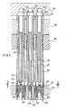
- the gripping means comprise pliers having four legs arranged in pairs facing one another and each pairs being perpendicular to each other (see Fig. 3).
- the microcomponents contained in magazines 52 form stacks which are generally indicated at 50.
- the microcomponents arranged at the end of each stack have b.een respectively indicated by the reference numeral 41a, 41b, 41c.
- the gripping means comprise four legs forming two pairs 43, 44 and 43', 44', respectively, which at the gripping zone are configurated to receive the respective microcomponent 41a, 41b, 4lc.
- Means 43', 44' differ from means 43, 44 only because of their shape. As a matter of fact they can have any shape provided that they would carry on the gripping function.
- FIGs. 5, 6 and 7 another type of gripping member comprising legs 20, 21, 22 and 23 is shown. These legs are configurated to grip through legs 21 and 23 a microcomponent provided with pins so as not to damage the electric terminals.
- Said gripping means which will be hereinafter referred to as pliers, have internally a hole 40.
- Plungers 45 are positioned inside said hole 40 throughout the length of the pliers, such plungers terminating with an enlarged flat end 42 forming a collar 42 against which the microcomponent will abut.
- Figs. 1 and 2 the zeroing plate 47, the pliers support plate 48 and the operating plate 49 are shown.
- the mutual movement of these plates to allow the gripping of the microcomponents are as follows: the support plate 48 supports the pliers so that the ends of the latter form a housing for the microcomponent 41a, 41b, 41c, being arranged at the free top openings 55 of magazines 52.
- the operation plate 49 is arranged at the narrowest portion of the pliers legs, so that the microcomponents 41a, 41b, 41c can be received therein.
- Fig. 2 shows the second step of the process: the pushers 65 push the stack 50 of components until the microcomponent 41a, 41b, 41c abuts against the surface 42 of the plunger, which in turn abuts against the bearing plate 48, then the pliers 43, 44 and 43' , 44', respectively, grip the respective microcomponent 41a, 41b, 41c. This is provided by causing the operating plate 49 to slide towards the thickest zone of the pliers, so that the pliers are closed.
- a cavity is internally formed, in which cavity 60 the end head 61 of plunger 45 is positioned.
- the positioning of the microcomponent 41a, 41b, 41c within the cavities 60 enables to signal that the microcomponent has been gripped.
- a first embodiment provides that the signalling occurs by a change in capacity of a capacitor.
- the plates of said capacitor comprise the metalized surface of the end head 61 and the metalized surface of cavity 60, while the dielectris is constituted by air.
- a second embodiment provides that within said metalized cavity 60 conductive terminals 62 and 64 can be obtained. Then, the movement of the end head 61 closes one of these contacts.
- a further embodiment of the present invention provides that, where desiring to check the functional efficiency of the microcomponent and hence to carry out electrical measurements, the plunger 45' (Fig. 4) and relative collar 30' comprise two conductive parts 31 and 32, which are suitably insulated from each other by means of insulation 33 and located at the terminals 34 of the microcomponent 41c:
- a further embodiment provides that the pliers (43, 44 and 43', 44') wich are suitably insulated also with respect to the pliers operating plate 49 and support plate 48, are the electric terminals through which the electric efficiency of the microcomponent is tested.
- This alarm signal can also indicate the coordinates on the printed circuit board where the microcomponent lacks, as it has not been gripped by the pliers.
- the above described gripping means can be provided as serially connected, so as to grip and check all the microcomponents required for a given printed circuit board.
Landscapes
- Engineering & Computer Science (AREA)
- Manufacturing & Machinery (AREA)
- Microelectronics & Electronic Packaging (AREA)
- Tests Of Electronic Circuits (AREA)
- Testing Of Short-Circuits, Discontinuities, Leakage, Or Incorrect Line Connections (AREA)
- Supply And Installment Of Electrical Components (AREA)
- Testing Electric Properties And Detecting Electric Faults (AREA)
Priority Applications (1)
| Application Number | Priority Date | Filing Date | Title |
|---|---|---|---|
| AT81108793T ATE23011T1 (de) | 1980-11-10 | 1981-10-23 | Verfahren und vorrichtung zum pruefen der anwesenheit und/oder der funktionstuechtigkeit von mikrobauelementen waehrend ihrer montage auf leiterplatten. |
Applications Claiming Priority (2)
| Application Number | Priority Date | Filing Date | Title |
|---|---|---|---|
| IT25854/80A IT1133771B (it) | 1980-11-10 | 1980-11-10 | Procedimento e apparecchiatura atti a verificare la presenza e/o efficienza di componenti a chip durante il loro montaggio su circuiti stampati |
| IT2585480 | 1980-11-10 |
Publications (2)
| Publication Number | Publication Date |
|---|---|
| EP0051777A1 true EP0051777A1 (de) | 1982-05-19 |
| EP0051777B1 EP0051777B1 (de) | 1986-10-15 |
Family
ID=11217934
Family Applications (1)
| Application Number | Title | Priority Date | Filing Date |
|---|---|---|---|
| EP81108793A Expired EP0051777B1 (de) | 1980-11-10 | 1981-10-23 | Verfahren und Vorrichtung zum Prüfen der Anwesenheit und/oder der Funktionstüchtigkeit von Mikrobauelementen während ihrer Montage auf Leiterplatten |
Country Status (7)
| Country | Link |
|---|---|
| US (1) | US4479089A (de) |
| EP (1) | EP0051777B1 (de) |
| JP (1) | JPS57109396A (de) |
| AT (1) | ATE23011T1 (de) |
| CA (1) | CA1181869A (de) |
| DE (1) | DE3175494D1 (de) |
| IT (1) | IT1133771B (de) |
Cited By (1)
| Publication number | Priority date | Publication date | Assignee | Title |
|---|---|---|---|---|
| FR2733172A1 (fr) * | 1995-04-12 | 1996-10-25 | Sillner Kamilla | Dispositif destine a etre utilise dans un appareil ou dans un systeme pour le traitement de composants, en particulier pour le traitement de composants electriques a semi-conducteurs |
Families Citing this family (3)
| Publication number | Priority date | Publication date | Assignee | Title |
|---|---|---|---|---|
| US4593820A (en) * | 1984-03-28 | 1986-06-10 | International Business Machines Corporation | Robotic, in-transit, device tester/sorter |
| US5606251A (en) * | 1994-07-15 | 1997-02-25 | Ontrak Systems, Inc. | Method and apparatus for detecting a substrate in a substrate processing system |
| DE10009386B4 (de) * | 2000-02-29 | 2005-09-08 | INSTITUT FüR MIKROTECHNIK MAINZ GMBH | Magazin, Montagevorrichtung für Mikrobauteile und Verfahren zum Montieren von Mikrobauteilen |
Citations (1)
| Publication number | Priority date | Publication date | Assignee | Title |
|---|---|---|---|---|
| US3731867A (en) * | 1971-07-19 | 1973-05-08 | Motorola Inc | Vacuum die sensor apparatus and method for a semiconductor die bonding machine |
Family Cites Families (3)
| Publication number | Priority date | Publication date | Assignee | Title |
|---|---|---|---|---|
| US2965229A (en) * | 1957-12-26 | 1960-12-20 | Sylvania Electric Prod | Lamp inspection apparatus |
| US4240032A (en) * | 1977-10-31 | 1980-12-16 | Western Electric Company, Inc. | Transporting and orienting an article using a movable carrier inserted into an indentation in the article |
| US4255955A (en) * | 1979-03-09 | 1981-03-17 | Chunzu Machinery Industry Co., Ltd. | Automatic safety mechanism for forming machines |
-
1980
- 1980-11-10 IT IT25854/80A patent/IT1133771B/it active
-
1981
- 1981-10-23 DE DE8181108793T patent/DE3175494D1/de not_active Expired
- 1981-10-23 EP EP81108793A patent/EP0051777B1/de not_active Expired
- 1981-10-23 AT AT81108793T patent/ATE23011T1/de not_active IP Right Cessation
- 1981-11-05 US US06/318,365 patent/US4479089A/en not_active Expired - Fee Related
- 1981-11-09 JP JP56178465A patent/JPS57109396A/ja active Pending
- 1981-11-09 CA CA000389706A patent/CA1181869A/en not_active Expired
Patent Citations (1)
| Publication number | Priority date | Publication date | Assignee | Title |
|---|---|---|---|---|
| US3731867A (en) * | 1971-07-19 | 1973-05-08 | Motorola Inc | Vacuum die sensor apparatus and method for a semiconductor die bonding machine |
Cited By (1)
| Publication number | Priority date | Publication date | Assignee | Title |
|---|---|---|---|---|
| FR2733172A1 (fr) * | 1995-04-12 | 1996-10-25 | Sillner Kamilla | Dispositif destine a etre utilise dans un appareil ou dans un systeme pour le traitement de composants, en particulier pour le traitement de composants electriques a semi-conducteurs |
Also Published As
| Publication number | Publication date |
|---|---|
| CA1181869A (en) | 1985-01-29 |
| US4479089A (en) | 1984-10-23 |
| IT8025854A0 (it) | 1980-11-10 |
| IT1133771B (it) | 1986-07-09 |
| DE3175494D1 (en) | 1986-11-20 |
| ATE23011T1 (de) | 1986-11-15 |
| EP0051777B1 (de) | 1986-10-15 |
| JPS57109396A (en) | 1982-07-07 |
Similar Documents
| Publication | Publication Date | Title |
|---|---|---|
| EP0107906B1 (de) | Fassung für integrierte Schaltungen | |
| US4090667A (en) | Universally programmable shorting plug for an integrated circuit socket | |
| US3963301A (en) | Mother-board interconnection system | |
| US4089041A (en) | Circuit programming device | |
| EP0342961A2 (de) | Bestücken von lichtemittierenden Dioden | |
| US4460236A (en) | Test apparatus for electrical circuit boards | |
| JP2761562B2 (ja) | Icハンドラのic搬送キャリア | |
| EP0051777A1 (de) | Verfahren und Vorrichtung zum Prüfen der Anwesenheit und/oder der Funktionstüchtigkeit von Mikrobauelementen während ihrer Montage auf Leiterplatten | |
| EP0741918B1 (de) | Chipkartenverbinder | |
| US4470652A (en) | Modular electrical shunts for integrated circuit applications | |
| US4933812A (en) | Package and circuit arrangement for housing and connecting polarized electrical components and method of manufacture | |
| EP0044519A1 (de) | Vorrichtung und Verfahren zum Aufsetzen elektrischer Mikroelemente auf eine gedruckte Schaltungsplatte | |
| JPH05288803A (ja) | Icトレー | |
| JPH06104600A (ja) | コネクタの挿着方法とその自動挿着装置 | |
| US7833043B2 (en) | Socket connector | |
| JPS5721848A (en) | Semiconductor device | |
| JPH07130801A (ja) | 半導体ic試験装置におけるハンドラ測定用ソケット。 | |
| JPH024472Y2 (de) | ||
| JPH012333A (ja) | 素子収納用トレイ | |
| SU1649692A1 (ru) | Контактное устройство дл контрол микросхем | |
| JPS649377A (en) | Testing method and sheet for integrated circuit package | |
| JPH05275503A (ja) | 電気機器およびその電気特性検査方法 | |
| JPS62123372A (ja) | 電子部品の測定体 | |
| JPH0629027U (ja) | コネクタ | |
| JPH07111992B2 (ja) | 素子収納用トレイ |
Legal Events
| Date | Code | Title | Description |
|---|---|---|---|
| PUAI | Public reference made under article 153(3) epc to a published international application that has entered the european phase |
Free format text: ORIGINAL CODE: 0009012 |
|
| AK | Designated contracting states |
Designated state(s): AT CH DE FR GB IT LI NL SE |
|
| 17P | Request for examination filed |
Effective date: 19821202 |
|
| R17P | Request for examination filed (corrected) |
Effective date: 19821120 |
|
| GRAA | (expected) grant |
Free format text: ORIGINAL CODE: 0009210 |
|
| AK | Designated contracting states |
Kind code of ref document: B1 Designated state(s): AT CH DE FR GB IT LI NL SE |
|
| PG25 | Lapsed in a contracting state [announced via postgrant information from national office to epo] |
Ref country code: NL Effective date: 19861015 Ref country code: LI Effective date: 19861015 Ref country code: IT Free format text: LAPSE BECAUSE OF FAILURE TO SUBMIT A TRANSLATION OF THE DESCRIPTION OR TO PAY THE FEE WITHIN THE PRESCRIBED TIME-LIMIT;WARNING: LAPSES OF ITALIAN PATENTS WITH EFFECTIVE DATE BEFORE 2007 MAY HAVE OCCURRED AT ANY TIME BEFORE 2007. THE CORRECT EFFECTIVE DATE MAY BE DIFFERENT FROM THE ONE RECORDED. Effective date: 19861015 Ref country code: FR Free format text: THE PATENT HAS BEEN ANNULLED BY A DECISION OF A NATIONAL AUTHORITY Effective date: 19861015 Ref country code: CH Effective date: 19861015 Ref country code: AT Effective date: 19861015 |
|
| REF | Corresponds to: |
Ref document number: 23011 Country of ref document: AT Date of ref document: 19861115 Kind code of ref document: T |
|
| PG25 | Lapsed in a contracting state [announced via postgrant information from national office to epo] |
Ref country code: SE Effective date: 19861031 |
|
| REF | Corresponds to: |
Ref document number: 3175494 Country of ref document: DE Date of ref document: 19861120 |
|
| RAP2 | Party data changed (patent owner data changed or rights of a patent transferred) |
Owner name: FERCO S.R.L. |
|
| REG | Reference to a national code |
Ref country code: CH Ref legal event code: PL |
|
| EN | Fr: translation not filed | ||
| NLV1 | Nl: lapsed or annulled due to failure to fulfill the requirements of art. 29p and 29m of the patents act | ||
| PG25 | Lapsed in a contracting state [announced via postgrant information from national office to epo] |
Ref country code: DE Effective date: 19870701 |
|
| PLBE | No opposition filed within time limit |
Free format text: ORIGINAL CODE: 0009261 |
|
| STAA | Information on the status of an ep patent application or granted ep patent |
Free format text: STATUS: NO OPPOSITION FILED WITHIN TIME LIMIT |
|
| GBPC | Gb: european patent ceased through non-payment of renewal fee | ||
| 26N | No opposition filed | ||
| PG25 | Lapsed in a contracting state [announced via postgrant information from national office to epo] |
Ref country code: GB Free format text: LAPSE BECAUSE OF NON-PAYMENT OF DUE FEES Effective date: 19881118 |