EP0054317A1 - Procédé de diffusion de l'aluminium dans un corps en silicium à partir d'une couche contenant de l'aluminium - Google Patents
Procédé de diffusion de l'aluminium dans un corps en silicium à partir d'une couche contenant de l'aluminium Download PDFInfo
- Publication number
- EP0054317A1 EP0054317A1 EP81201282A EP81201282A EP0054317A1 EP 0054317 A1 EP0054317 A1 EP 0054317A1 EP 81201282 A EP81201282 A EP 81201282A EP 81201282 A EP81201282 A EP 81201282A EP 0054317 A1 EP0054317 A1 EP 0054317A1
- Authority
- EP
- European Patent Office
- Prior art keywords
- aluminium
- parts
- diffusion treatment
- region
- aluminium source
- Prior art date
- Legal status (The legal status is an assumption and is not a legal conclusion. Google has not performed a legal analysis and makes no representation as to the accuracy of the status listed.)
- Granted
Links
Images
Classifications
-
- H—ELECTRICITY
- H10—SEMICONDUCTOR DEVICES; ELECTRIC SOLID-STATE DEVICES NOT OTHERWISE PROVIDED FOR
- H10P—GENERIC PROCESSES OR APPARATUS FOR THE MANUFACTURE OR TREATMENT OF DEVICES COVERED BY CLASS H10
- H10P32/00—Diffusion of dopants within, into or out of wafers, substrates or parts of devices
- H10P32/10—Diffusion of dopants within, into or out of semiconductor bodies or layers
- H10P32/17—Diffusion of dopants within, into or out of semiconductor bodies or layers characterised by the semiconductor material
- H10P32/171—Diffusion of dopants within, into or out of semiconductor bodies or layers characterised by the semiconductor material being group IV material
-
- H—ELECTRICITY
- H10—SEMICONDUCTOR DEVICES; ELECTRIC SOLID-STATE DEVICES NOT OTHERWISE PROVIDED FOR
- H10P—GENERIC PROCESSES OR APPARATUS FOR THE MANUFACTURE OR TREATMENT OF DEVICES COVERED BY CLASS H10
- H10P32/00—Diffusion of dopants within, into or out of wafers, substrates or parts of devices
- H10P32/10—Diffusion of dopants within, into or out of semiconductor bodies or layers
- H10P32/14—Diffusion of dopants within, into or out of semiconductor bodies or layers within a single semiconductor body or layer in a solid phase; between different semiconductor bodies or layers, both in a solid phase
- H10P32/1408—Diffusion of dopants within, into or out of semiconductor bodies or layers within a single semiconductor body or layer in a solid phase; between different semiconductor bodies or layers, both in a solid phase from or through or into an external applied layer, e.g. photoresist or nitride layers
-
- H—ELECTRICITY
- H10—SEMICONDUCTOR DEVICES; ELECTRIC SOLID-STATE DEVICES NOT OTHERWISE PROVIDED FOR
- H10W—GENERIC PACKAGES, INTERCONNECTIONS, CONNECTORS OR OTHER CONSTRUCTIONAL DETAILS OF DEVICES COVERED BY CLASS H10
- H10W10/00—Isolation regions in semiconductor bodies between components of integrated devices
- H10W10/01—Manufacture or treatment
- H10W10/031—Manufacture or treatment of isolation regions comprising PN junctions
-
- H—ELECTRICITY
- H10—SEMICONDUCTOR DEVICES; ELECTRIC SOLID-STATE DEVICES NOT OTHERWISE PROVIDED FOR
- H10W—GENERIC PACKAGES, INTERCONNECTIONS, CONNECTORS OR OTHER CONSTRUCTIONAL DETAILS OF DEVICES COVERED BY CLASS H10
- H10W10/00—Isolation regions in semiconductor bodies between components of integrated devices
- H10W10/30—Isolation regions comprising PN junctions
Definitions
- the invention relates to a method of manufacturing a semiconductor device in which an aluminium-containing layer, hereinafter referred to as the aluminium source, is locally provided on a semiconductor body of silicon and in a subsequent diffusion treatment aluminium is diffused from the aluminium source into the silicon body and an aluminium-doped_region is formed in the silicor body.
- an aluminium-containing layer hereinafter referred to as the aluminium source
- an aluminium layer is provided on a silicon body, which layer is restricted, by means of photoetching methods, to locations where said layer will serve as a doping source in a diffusion treatment.
- Diffusion treatments in which an aluminium sourc is provided directly on a silicon surface have not obtaine the popularity which they deserve from a point of view of their simplicity, for example, with respect to a diffusion treatment in a closed ampoule with a diffusion source consisting of aluminium-containing silicon powder.
- Such a region often shows bulges both in the depth direction and also in the laterial direction.
- aluminium-doped regions formed regularly and reproducibly both in the depth direction and in the lateral direction are obtained. Drop formation in the aluminium layer and undesired interruptions in the doped region are avoided, while an oxide layer formed during the diffusion can easily be removed.
- the aluminium source is preferably given a shape corresponding to the shape of the doped region to be formed and is simultaneously divided into the said parts.
- the surface of the parts of the aluminium source is preferably given dimensions of approx. 6 / um x 6 / um.
- the removal of an oxide layer present on the aluminium layer after the diffusion treatment in the said first modified embodiment is very complete when, preceding the diffusion treatment, the formed parts are subjected to an etching treatment in which oxide is removed from the surface of the parts.
- the said second modified embodiment gives very clear results in particular when the thickness of the aluminium source is chosen to be at most equal to O.2 / um.
- the size of the parts is determined by the grain size of the aluminium of the aluminium source.
- the mutual distance of the parts obtained by means of the last-mentioned modified embodiment is sufficient to avoid the above-described problems at least to a considerable extent.
- a particularly favourable result can be obtained with a very short etching treatment, for example, in an etching bath consisting of a solution of hydrogen fluoride in water in approximately 30 seconds.
- Semiconductor devices having thick epitaxial layers for example, bipolar transistors with high collector-emitter voltages with open base, can be made by means of the method in accordance with the invention.
- the diffusion treatment is preferably carried out in an oxidizing atmosphere.
- An oxide layer is formed on the source and the free surface of the silicon body.
- the diffusion treatment is preferably completed by a second diffusion treatment in whdch, at a part of the surface of the silicon body separated from the first-mentioned region, a second region is formed by means of boron as a dopant and having a smaller depth than the first region, and the surface of the first region is simultaneously subjected to the second diffusion treatment.
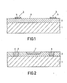
- Figures 1 and 2 are diagrammatic sectional views of a part of a semiconductor device in successive stages of its manufacture by means of the method according to the invention.
- the aluminium source 3 is divided, prior to the diffusion treatment, into parts 5 each having an area which is small as compared with the surface area of the region 4 to be formed.
- the mutual distance of the parts 5 is smaller than double the distance over which the aluminium during the diffusion treatment diffuses laterally into the silicon body 1,2.
- the parts 5 are so small that their uninterrupted shape during the diffusion treatment remains unvaried.
- both in the direction of depth and in the laterial direction regions are obtained which are regularly and reproducibly doped with aluminium. Drop formation in the aluminium layer and undesired interruptions in the doped region are avoided. An oxide layer formed on the aluminium during the diffusion can easily be removed.
- the division of the aluminium source 3 into the parts 5 can take place simultaneously with the d*esing of the source 3 itself, namely in the same photoetching step.
- This method is used in particular when the thickness of the source is not very small, preferably larger than O.5 / um.
- the division of the aluminium source 3 into the parts 5 may also take place after the design of the source 3, namely by a treatment in which the grain boundaries in the aluminium source are etched preferentially. This method is used in particular when the thickness of the source is not too large, and preferably is smaller than 0.2/um.
- the silicon body is preferably formed by providing an n-type conductive epitaxial layer 2 on a p-type conductive substrate 1 and the doped region 4 is formal by diffusion from the free surface 6 of the epitaxial layer 2 throughout the thickness of said epitaxial layer.
- the aluminium content at the free surface of the doped region 4 is lower than in deeper- located parts of the region.
- Starting material in the manufacture is, for example, a 450 / um thick p-type conductive substrate 1 having a resistivity of 35 ⁇ cm. On said substrate is deposited in a usual manner a 40 / um thick n-type conductive epitaxial layer 2 having a resistivity of 40 ⁇ cm.
- boron is diffused at the area of the region 4 and elsewhere via the surface 6, so that the concentration in the region 4 is replenished again, and in the epitaxial layer 2 the second region 7 is formed which may serve as a base of the transistor.
- Boron may be diffused in the usual manner starting from boron bromide as a source for 4 hours at 1,160°C.
- the second region 7 is, for example, 6ium deep.
Landscapes
- Weting (AREA)
- Electrodes Of Semiconductors (AREA)
Applications Claiming Priority (2)
| Application Number | Priority Date | Filing Date | Title |
|---|---|---|---|
| NL8006668A NL8006668A (nl) | 1980-12-09 | 1980-12-09 | Werkwijze voor het vervaardigen van een halfgeleiderinrichting. |
| NL8006668 | 1980-12-09 |
Publications (2)
| Publication Number | Publication Date |
|---|---|
| EP0054317A1 true EP0054317A1 (fr) | 1982-06-23 |
| EP0054317B1 EP0054317B1 (fr) | 1985-02-20 |
Family
ID=19836296
Family Applications (1)
| Application Number | Title | Priority Date | Filing Date |
|---|---|---|---|
| EP81201282A Expired EP0054317B1 (fr) | 1980-12-09 | 1981-11-20 | Procédé de diffusion de l'aluminium dans un corps en silicium à partir d'une couche contenant de l'aluminium |
Country Status (6)
| Country | Link |
|---|---|
| US (1) | US4381957A (fr) |
| EP (1) | EP0054317B1 (fr) |
| JP (1) | JPS57121222A (fr) |
| DE (1) | DE3169109D1 (fr) |
| IE (1) | IE52979B1 (fr) |
| NL (1) | NL8006668A (fr) |
Cited By (1)
| Publication number | Priority date | Publication date | Assignee | Title |
|---|---|---|---|---|
| EP0216954A1 (fr) * | 1985-06-10 | 1987-04-08 | BBC Brown Boveri AG | Procédé pour le dopage en aluminium d'un dispositif semi-conducteur |
Families Citing this family (5)
| Publication number | Priority date | Publication date | Assignee | Title |
|---|---|---|---|---|
| JPH0693509B2 (ja) * | 1983-08-26 | 1994-11-16 | シャープ株式会社 | 薄膜トランジスタ |
| EP0263270B1 (fr) * | 1986-09-30 | 1992-11-11 | Siemens Aktiengesellschaft | Procédé de réalisation d'une région semi-conductrice dopée P dans un corps semi-conducteur de conductivité N |
| EP0262356B1 (fr) * | 1986-09-30 | 1993-03-31 | Siemens Aktiengesellschaft | Méthode de fabrication d'une jonction P-N à haute tenue en tension |
| US8481414B2 (en) * | 2011-04-08 | 2013-07-09 | Micron Technology, Inc. | Incorporating impurities using a discontinuous mask |
| CN113053736B (zh) * | 2021-03-11 | 2024-05-03 | 捷捷半导体有限公司 | 一种半导体器件制作方法 |
Citations (3)
| Publication number | Priority date | Publication date | Assignee | Title |
|---|---|---|---|---|
| FR2301093A1 (fr) * | 1975-02-15 | 1976-09-10 | Itt | Methode de diffusion de regions isolantes dans un substrat semi-conducteur |
| US4021269A (en) * | 1975-11-26 | 1977-05-03 | General Electric Company | Post diffusion after temperature gradient zone melting |
| DE1811277B2 (de) * | 1968-11-27 | 1977-09-08 | Siemens AG, 1000 Berlin und 8000 München | Verfahren zum herstellen von p-dotierten zonen mit unterschiedlichen eindringtiefen in einer n-silicium- schicht |
Family Cites Families (9)
| Publication number | Priority date | Publication date | Assignee | Title |
|---|---|---|---|---|
| DE1227154B (de) * | 1963-07-23 | 1966-10-20 | Siemens Ag | Verfahren zur Herstellung eines pn-UEbergangs in einer einkristallinen Halbleiteranordnung |
| FR1495766A (fr) * | 1965-12-10 | 1967-12-20 | ||
| GB1536545A (en) * | 1975-03-26 | 1978-12-20 | Mullard Ltd | Semiconductor device manufacture |
| US3998662A (en) * | 1975-12-31 | 1976-12-21 | General Electric Company | Migration of fine lines for bodies of semiconductor materials having a (100) planar orientation of a major surface |
| JPS5310265A (en) * | 1976-07-15 | 1978-01-30 | Mitsubishi Electric Corp | Impurity diffusion method |
| US4066485A (en) * | 1977-01-21 | 1978-01-03 | Rca Corporation | Method of fabricating a semiconductor device |
| JPS53118367A (en) * | 1977-03-25 | 1978-10-16 | Hitachi Ltd | Manufacture of semiconductor |
| JPS54144889A (en) * | 1978-05-04 | 1979-11-12 | Hitachi Ltd | Manufacture for semiconductor device |
| JPS55140241A (en) * | 1979-04-19 | 1980-11-01 | Matsushita Electronics Corp | Method of fabricating semiconductor device |
-
1980
- 1980-12-09 NL NL8006668A patent/NL8006668A/nl not_active Application Discontinuation
-
1981
- 1981-11-16 US US06/321,960 patent/US4381957A/en not_active Expired - Fee Related
- 1981-11-20 EP EP81201282A patent/EP0054317B1/fr not_active Expired
- 1981-11-20 DE DE8181201282T patent/DE3169109D1/de not_active Expired
- 1981-12-05 JP JP56195137A patent/JPS57121222A/ja active Granted
- 1981-12-07 IE IE2870/81A patent/IE52979B1/en not_active IP Right Cessation
Patent Citations (3)
| Publication number | Priority date | Publication date | Assignee | Title |
|---|---|---|---|---|
| DE1811277B2 (de) * | 1968-11-27 | 1977-09-08 | Siemens AG, 1000 Berlin und 8000 München | Verfahren zum herstellen von p-dotierten zonen mit unterschiedlichen eindringtiefen in einer n-silicium- schicht |
| FR2301093A1 (fr) * | 1975-02-15 | 1976-09-10 | Itt | Methode de diffusion de regions isolantes dans un substrat semi-conducteur |
| US4021269A (en) * | 1975-11-26 | 1977-05-03 | General Electric Company | Post diffusion after temperature gradient zone melting |
Cited By (1)
| Publication number | Priority date | Publication date | Assignee | Title |
|---|---|---|---|---|
| EP0216954A1 (fr) * | 1985-06-10 | 1987-04-08 | BBC Brown Boveri AG | Procédé pour le dopage en aluminium d'un dispositif semi-conducteur |
Also Published As
| Publication number | Publication date |
|---|---|
| EP0054317B1 (fr) | 1985-02-20 |
| IE812870L (en) | 1983-06-09 |
| US4381957A (en) | 1983-05-03 |
| IE52979B1 (en) | 1988-04-27 |
| JPS6262457B2 (fr) | 1987-12-26 |
| JPS57121222A (en) | 1982-07-28 |
| NL8006668A (nl) | 1982-07-01 |
| DE3169109D1 (en) | 1985-03-28 |
Similar Documents
| Publication | Publication Date | Title |
|---|---|---|
| US4375999A (en) | Method of manufacturing a semiconductor device | |
| US3664896A (en) | Deposited silicon diffusion sources | |
| US4536945A (en) | Process for producing CMOS structures with Schottky bipolar transistors | |
| US4481706A (en) | Process for manufacturing integrated bi-polar transistors of very small dimensions | |
| US4124934A (en) | Manufacture of semiconductor devices in which a doping impurity is diffused from a polycrystalline semiconductor layer into an underlying monocrystalline semiconductor material, and semiconductor devices thus manufactured | |
| US4060427A (en) | Method of forming an integrated circuit region through the combination of ion implantation and diffusion steps | |
| US3753807A (en) | Manufacture of bipolar semiconductor devices | |
| US5682052A (en) | Method for forming isolated intra-polycrystalline silicon structure | |
| US4408387A (en) | Method for producing a bipolar transistor utilizing an oxidized semiconductor masking layer in conjunction with an anti-oxidation mask | |
| US4354307A (en) | Method for mass producing miniature field effect transistors in high density LSI/VLSI chips | |
| JPS5879762A (ja) | サブミクロンバイポ−ラトランジスタ及びその製造方法 | |
| EP0051534A2 (fr) | Procédé de fabrication auto-alignée de structures de circuits intégrés employant différents taux de croissance de l'oxyde | |
| EP0054317B1 (fr) | Procédé de diffusion de l'aluminium dans un corps en silicium à partir d'une couche contenant de l'aluminium | |
| JPH06318676A (ja) | 半導体装置の製造方法 | |
| JP3252397B2 (ja) | 配線形成方法 | |
| JP2565162B2 (ja) | バイポ−ラトランジスタおよびその製造方法 | |
| US4546537A (en) | Method for producing a semiconductor device utilizing V-groove etching and thermal oxidation | |
| JP3091800B2 (ja) | Soi基板の製造方法 | |
| JPH0648690B2 (ja) | 半導体装置の製造方法 | |
| US4679306A (en) | Self-aligned process for forming dielectrically isolating regions formed in semiconductor device | |
| JPS6161268B2 (fr) | ||
| JP2576664B2 (ja) | Npnトランジスタの製造方法 | |
| JPH01238144A (ja) | 半導体装置の製造方法 | |
| GB2115609A (en) | Semiconductor structure manufacturing method | |
| JP2002118261A (ja) | 半導体装置及びその製造方法 |
Legal Events
| Date | Code | Title | Description |
|---|---|---|---|
| PUAI | Public reference made under article 153(3) epc to a published international application that has entered the european phase |
Free format text: ORIGINAL CODE: 0009012 |
|
| AK | Designated contracting states |
Designated state(s): DE FR GB NL |
|
| RAP1 | Party data changed (applicant data changed or rights of an application transferred) |
Owner name: N.V. PHILIPS' GLOEILAMPENFABRIEKEN |
|
| 17P | Request for examination filed |
Effective date: 19820824 |
|
| GRAA | (expected) grant |
Free format text: ORIGINAL CODE: 0009210 |
|
| AK | Designated contracting states |
Designated state(s): DE FR GB NL |
|
| REF | Corresponds to: |
Ref document number: 3169109 Country of ref document: DE Date of ref document: 19850328 |
|
| ET | Fr: translation filed | ||
| PLBE | No opposition filed within time limit |
Free format text: ORIGINAL CODE: 0009261 |
|
| STAA | Information on the status of an ep patent application or granted ep patent |
Free format text: STATUS: NO OPPOSITION FILED WITHIN TIME LIMIT |
|
| 26N | No opposition filed | ||
| PGFP | Annual fee paid to national office [announced via postgrant information from national office to epo] |
Ref country code: NL Payment date: 19891130 Year of fee payment: 9 |
|
| PGFP | Annual fee paid to national office [announced via postgrant information from national office to epo] |
Ref country code: FR Payment date: 19901123 Year of fee payment: 10 |
|
| PGFP | Annual fee paid to national office [announced via postgrant information from national office to epo] |
Ref country code: DE Payment date: 19910125 Year of fee payment: 10 |
|
| PG25 | Lapsed in a contracting state [announced via postgrant information from national office to epo] |
Ref country code: NL Effective date: 19910601 |
|
| NLV4 | Nl: lapsed or anulled due to non-payment of the annual fee | ||
| PGFP | Annual fee paid to national office [announced via postgrant information from national office to epo] |
Ref country code: GB Payment date: 19911031 Year of fee payment: 11 |
|
| PG25 | Lapsed in a contracting state [announced via postgrant information from national office to epo] |
Ref country code: FR Effective date: 19920731 |
|
| PG25 | Lapsed in a contracting state [announced via postgrant information from national office to epo] |
Ref country code: DE Effective date: 19920801 |
|
| REG | Reference to a national code |
Ref country code: FR Ref legal event code: ST |
|
| PG25 | Lapsed in a contracting state [announced via postgrant information from national office to epo] |
Ref country code: GB Effective date: 19921120 |
|
| GBPC | Gb: european patent ceased through non-payment of renewal fee |
Effective date: 19921120 |
|
| REG | Reference to a national code |
Ref country code: FR Ref legal event code: TP |