EP0055323A2 - Einrichtung zum Löten von chipartigen Bauteilen - Google Patents
Einrichtung zum Löten von chipartigen Bauteilen Download PDFInfo
- Publication number
- EP0055323A2 EP0055323A2 EP81106768A EP81106768A EP0055323A2 EP 0055323 A2 EP0055323 A2 EP 0055323A2 EP 81106768 A EP81106768 A EP 81106768A EP 81106768 A EP81106768 A EP 81106768A EP 0055323 A2 EP0055323 A2 EP 0055323A2
- Authority
- EP
- European Patent Office
- Prior art keywords
- solder
- nozzle
- printed circuit
- circuit board
- nozzles
- Prior art date
- Legal status (The legal status is an assumption and is not a legal conclusion. Google has not performed a legal analysis and makes no representation as to the accuracy of the status listed.)
- Granted
Links
Images




Classifications
-
- B—PERFORMING OPERATIONS; TRANSPORTING
- B23—MACHINE TOOLS; METAL-WORKING NOT OTHERWISE PROVIDED FOR
- B23K—SOLDERING OR UNSOLDERING; WELDING; CLADDING OR PLATING BY SOLDERING OR WELDING; CUTTING BY APPLYING HEAT LOCALLY, e.g. FLAME CUTTING; WORKING BY LASER BEAM
- B23K1/00—Soldering, e.g. brazing, or unsoldering
- B23K1/08—Soldering by means of dipping in molten solder
-
- B—PERFORMING OPERATIONS; TRANSPORTING
- B23—MACHINE TOOLS; METAL-WORKING NOT OTHERWISE PROVIDED FOR
- B23K—SOLDERING OR UNSOLDERING; WELDING; CLADDING OR PLATING BY SOLDERING OR WELDING; CUTTING BY APPLYING HEAT LOCALLY, e.g. FLAME CUTTING; WORKING BY LASER BEAM
- B23K3/00—Tools, devices or special appurtenances for soldering, e.g. brazing, or unsoldering, not specially adapted for particular methods
- B23K3/06—Solder feeding devices; Solder melting pans
- B23K3/0646—Solder baths
- B23K3/0653—Solder baths with wave generating means, e.g. nozzles, jets, fountains
-
- B—PERFORMING OPERATIONS; TRANSPORTING
- B23—MACHINE TOOLS; METAL-WORKING NOT OTHERWISE PROVIDED FOR
- B23K—SOLDERING OR UNSOLDERING; WELDING; CLADDING OR PLATING BY SOLDERING OR WELDING; CUTTING BY APPLYING HEAT LOCALLY, e.g. FLAME CUTTING; WORKING BY LASER BEAM
- B23K2101/00—Articles made by soldering, welding or cutting
- B23K2101/36—Electric or electronic devices
- B23K2101/42—Printed circuits
-
- H—ELECTRICITY
- H05—ELECTRIC TECHNIQUES NOT OTHERWISE PROVIDED FOR
- H05K—PRINTED CIRCUITS; CASINGS OR CONSTRUCTIONAL DETAILS OF ELECTRIC APPARATUS; MANUFACTURE OF ASSEMBLAGES OF ELECTRICAL COMPONENTS
- H05K3/00—Apparatus or processes for manufacturing printed circuits
- H05K3/30—Assembling printed circuits with electric components, e.g. with resistors
- H05K3/32—Assembling printed circuits with electric components, e.g. with resistors electrically connecting electric components or wires to printed circuits
- H05K3/34—Assembling printed circuits with electric components, e.g. with resistors electrically connecting electric components or wires to printed circuits by soldering
- H05K3/341—Surface mounted components
- H05K3/3431—Leadless components
- H05K3/3442—Leadless components having edge contacts, e.g. leadless chip capacitors, chip carriers
-
- H—ELECTRICITY
- H05—ELECTRIC TECHNIQUES NOT OTHERWISE PROVIDED FOR
- H05K—PRINTED CIRCUITS; CASINGS OR CONSTRUCTIONAL DETAILS OF ELECTRIC APPARATUS; MANUFACTURE OF ASSEMBLAGES OF ELECTRICAL COMPONENTS
- H05K3/00—Apparatus or processes for manufacturing printed circuits
- H05K3/30—Assembling printed circuits with electric components, e.g. with resistors
- H05K3/32—Assembling printed circuits with electric components, e.g. with resistors electrically connecting electric components or wires to printed circuits
- H05K3/34—Assembling printed circuits with electric components, e.g. with resistors electrically connecting electric components or wires to printed circuits by soldering
- H05K3/3465—Application of solder
- H05K3/3468—Application of molten solder, e.g. dip soldering
Definitions
- the present invention generally relates to a soldering process, anymore particularly, to a soldering process and a soldering apparatus employed therefor mainly dealing with printed circuit boards having chip type elements or components without leads such as resistors, capacitors or the like mounted thereon.
- soldering of the chip type components there has conventionally been employed a spouting type soldering system in which soldering is effected by spouting or applying molten solder onto a soldering surface of a printed circuit board during movement of the printed circuit board.
- the spouting type soldering system as described above is broadly divided into two systems according to configurations of the spouting solder waves, i.e.
- solder wave spouting type in which the solder wave is formed into an approximately symmetrical configuration with respect to a spouting port or nozzle for the molten solder
- the other system referred to as a single direction solder wave spouting type which provides a solder wave flowing in a direction counter to the direction of movement of the circuit printed board.
- soldering systems as described above, however, have serious disadvantages inherent therein. More specifically, in the former double direction solder wave spouting type, the solder wave 2 is spouted from the nozzle 1 in the-symmetrical configuration as shown in Fig. 1, while the printed circuit board 4, on which the chip type components 3 are mounted, is moved from left to right as indicated by an arrow in the figure. In the above arrangement, however, when the circuit board 4 leaves or exits from the solder wave 2, molten solder of the solder wave 2 tends to flow down in the same direction as the direction of movement of the printed circuit board 4, with excessive solder adhering to the chip type component 3, and thus, as shown in Fig. 2, excessive solder paddings i.e.
- fillets 9 higher in height than the chip component 3 are undesirably formed between electrode portions 6 of the chip component 3 mounted on the printed circuit board 4 by a bonding agent 5 and conductor portions 8 of the circuit board 4 surrounded by a solder resist layer 7.
- a bonding agent 5 As is seen from a graph of Fig. 3, when the finished printed circuit board 4 is subjected to deformation (bending) due to application of an external force or heat, cracks are readily formed within the chip type component 3, which is rigidly connected to the circuit board 4 by the excessive solder paddings 9, for possible deterioration of the characteristics thereof, and thus, giving rise to malfunctions of the circuit when the circuit board 4 is to be incorporated _into electronic appliances or the products are put into markets.
- solder wave 11 flows from a nozzle 10 in a direction counter to the direction of movement of the printed circuit board 4, while the circuit board 4 passes through the solder wave 11 along a path inclined upwardly with respect to the direction of movement thereof.
- molten solder of the solder wave 11 flows down in a direction counter to the direction of the circuit board movement so as to be dragged into said solder wave 11, without forming excessive paddings or fillets.
- solder wave 11 is directed only to one side with respect to the chip component 3, i.e. in the direction from right to left in Fig. 4, although a normal solder padding 13 not exceeding the height of the chip type component 3 is obtained at the forward portion 12 of the component 3 with respect to the advancing direction of the circuit board 4 as shown in Fig. 5, gas of flux evaporated during the soldering undesirably stays at the rear portion 14 of the component 3 without being removed therefrom, and thus, no molten solder adheres to such rear portion 14 inevitably requiring further manual solder padding work for correction at a later stage of processing.
- an essential object of the present invention is to provide an improved soldering process in which no manual corrections or repairing are required at later stages of processing, through elimination of faulty soldering of chip type components.
- Another important object of the present invention is to provide a soldering apparatus which is capable of readily effecting the soldering process as described above at high efficiency, even when chip type components of small size are mounted at high density on the printed circuit boards.
- a further object of the present invention is to provide a soldering apparatus of the above described type which is simple in construction and accurate in functioning at high reliability, and can be readily introduced into a production line at low cost.
- a process of soldering printed circuit boards including the steps of supplying molten solder into independent first and second nozzles so as to flow out therefrom, and effecting soldering by passing a printed circuit board in the order of the first nozzle.
- the-improvement of which comprises the steps of forming a first solder wave from the first nozzle at least in the direction of movement of the printed circuit board, and forming, at the second nozzle, a second solder wave higher in height than the first solder wave and flowing out from the second nozzle at least in a direction counter to the direction of movement of the printed circuit board, with the printed circuit board being moved in an inclined state so that the surface thereof contacts the first and second solder waves flowing out from the first and second nozzles, while there is also provided an apparatus for soldering the printed circuit boards for efficiently carrying out said soldering process even when small chip type components are mounted at high density on the printed circuit boards.
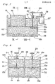
- a soldering apparatus G for effecting an improved soldering process which generally includes a housing or container 15 of a rectangular cubic box-like configuration having front and rear walls 15f and 15r, side walls 15c, and a bottom wall 15b, in which molten solder-16 is accommodated and which is divided into two similar molten solder sump portions 15A and 15B by a partition wall 35 extending between the front and rear walls 15f and 15r in a direction parallel to the side walls 15c generally at a central portion of the container 15, each of which sump portions 15A and 15B is further divided into upper and lower portions by another partition wall 15W laterally extending between the side walls 15c of the container 15, and a first solder spouting portion or nozzle 17 and a second solder spouting portion or nozzle 18 respectively provided in the corresponding sump portions 15A and 15B in the manner as described hereinbelow.
- the sump portion 15A for the first nozzle 17 has heater members 19 disposed adjacent to the bottom portion thereof, and an impeller 25 fixedly mounted at the lower end of a shaft 24 which extend: through a solder flow opening 01 formed in the lateral partition wall 15W of the container 15 and is rotatably supported in the sump portion 15A by a bearing member 23 secured to the front wall 15f of the container 15, and which is coupled, at.its upper end, to a motor 20 fixed to the outer side face of the front wall 15f through a belt and pulley drive 22 and a speed change gear 21, while the sump portion 15B for the second nozzle 18 is similarly provided with heater members 26, and an impeller 32 fixedly mounted at the lower end of another shaft 31 which also extends through another solder flow opening 02 formed in the lateral partition wall 15W and is rotatably supported in the sump portion 15B by a.bearing member 30
- first and second nozzles 17 and 18 respectively form a first solder wave 36 and a second solder wave 37 (Figs. 9 and 10) of the molten solder 16-which is fed out by the rotation of said impellers 29 and 32, while the height of the spouting solder waves 36 and 37 may be readily altered, since the respective motors 20 and 27 are provided with the speed change gears 21 and 28.
- the printed circuit board 4, on which chip type components 3 are mounted is advanced in the direction indicated by the arrow F and passes through the solder wave 36 from the first nozzle 17 and then, the solder wave 37 from the second nozzle 18.
- the molten solder 16 forming the first solder wave..36 flows down from a spouting port 17a of the first nozzle 17 in the direction of movement of the printed circuit board 4, and in this case, the solder wave 36 is applied to the front portion 3a (Fig. 10) of the chip type component 3 mounted on the circuit board 4 and forms a solder padding or fillet 38 thereat by driving away the flux gas developed.
- the solder wave 36 is also applied to the rear portion 3b of the chip type component 3, and forms a similar solder padding or fillet 39 thereat.
- the solder paddings 38 and 39 to be formed in the above case become excessive in the amounts thereof, since the direction of flow of the solder wave 36 is the same as the direction of movement of the printed circuit board 4.
- the molten solder 15 spouted from a spouting port 18a of the second nozzle 18 is checked or stopped by a check or dam portion 40 provided at the upper front edge of the second nozzle. 18 (Figs.
- the second solder wave 37 formed by the nozzle 18 is made larger in its height than the first solder wave 36, with the printed circuit board 4 being adapted to enter and.leave the second solder wave 37 in a state where it is inclined or raised upwards with respect to the advancing direction thereof, the excessive solder paddings 38 and 39 formed on the chip type component 3 by the first solder wave 36 of the nozzle 17, are removed or scraped off as they are passed through the second solder wave 37 so that the extra solder thereof is fused into the second solder wave 37, and thus, the excessive solder paddings 38 and 39 are rectified or corrected into normal solder paddings 41 of a small size as shown in Fig. 11.
- solder bridge means a soldering fault resulting from short-circuits between electrodes of neighboring chip type components, which requires manual corrections at latex stages of the processihg. From Table l,.it is noticed' that no soldering faults have taken place in the case of the embodiment according to the present invention.
- a distance l between the front upper edge 117a of the first nozzle 117 and the rear upper edge 118a of the second nozzle 118 was set to 5 cm in the experiments. If the distance l is excessively short, not only a smooth flow of the molten solder 16 is unavailable, but there may be cases where the solder does not sufficiently adhere due to difficulty'in efficiently releasing the gas to be developed during soldering.
- the distance l between the front upper edge 117a of the first nozzle 117 and the rear upper edge 118a of the second nozzle 118 is to be limited within the range practically applicable, and should desirably be larger than 3 cm and smaller than 20 cm, and more preferably, be larger than 5 cm and smaller than 15 cm.
- Fig. ' 12 may further be modified as in Fig. 13, in which control plates are provided in the vicinity of upper edges of the spouting ports for the nozzles for restricting the flow of the molten solder.
- first and second control plates 201 and 202 of predetermined shapes are respectively provided so as to extend towards each other for efficient control of the flow of the molten solder 16.
- a distance d between the front edge of the control plate 201 provided for the first nozzle 217 and the corresponding edge of the control plate 202 provided for the second nozzle 218 should be larger than 1 cm, and more preferably, larger than 2 cm.
- the lengths of the control plates 201 and 202 are respectively represented by Sl and S2 , it is preferable that the relation as follows are satisfied. or more preferably,
- tangential angles a, Sand y at the rear edges of the first nozzles 17B, 17C and 17D of various shapes, in the vicinity of the spouting ports thereof should suitably be 2 to 80°, respectively. If the angles ⁇ , ⁇ and ⁇ are smaller than 2 °, the pressure to be applied to the electrode portion of the component is reduced as in an ordinary spouting flow, while on the contrary, if the angles a, ⁇ and y are larger than 80°, there may arise such a problem that the end of the nozzle undesirably contacts the chip type components mounted on the printed circuit board.
- the above tangential angles a, ⁇ and y should more preferably be 5 to 60°. Meanwhile, in the experiments as described above, such results were also obtained that a better soldering yield was achieved when the bending directions of the first and second nozzles were opposite to each other.
- Table 3 shows the rate of occurrence of faulty soldering with respect to a predetermined mounting density of chip type components on the printed circuit board.
- the two nozzles 17 and 18 are arranged to be provided in one molten solder container 15 divided into the two sump portions 15A and 15B by the partition wall.35, the arrangement may of course be modified to provide the two nozzles in two separate molten . solder containers one by one, with the two separate molten solder containers being disposed side by side for association so as to achieve the similar effects as in the present embodiments.
- such two nozzles may be provided .in one molten solder container without any partition wall therein so as to form separate solder waves having different heights through the two nozzles with the use of one motor and one impeller.
- the size of the solder spouting ports of the two nozzles' should be altered. More specifically, by making the molten solder spouting port of the second nozzle smaller than that of the first nozzle, it is possible to render the height of_the second solder wave by the second nozzle higher than that of the first solder wave, and thus, effects similar to the embodiments described earlier may also be obtained.
- the first nozzle 317 and second nozzle 318 are so constructed, in the relation between the molten solder flow-in port areas thereof, that respective area ratios are represnented by a formula, where Al is a solder flow-in port area for the first nozzle 317, A2 is a-solder flow-in port area for the second nozzle 318 with respect to the direction F of movement of the printed circuit board, Vl and V2 are nozzle inner face volumes (hatched portions in Fig. 17) from the molten solder level to the respective solder flow-out ports, and K is a factor in the range of 0.1 to 1.2 related to the number of bending points or amount of solder leakage at the junction of sheet metals. If the factor K is smaller than 0.1, no molten solder overflows the first nozzle, while on the other hand, if the factor K exceeds 1.2, the amount of molten solder overflowing the second nozzle is reduced.
Landscapes
- Engineering & Computer Science (AREA)
- Mechanical Engineering (AREA)
- Molten Solder (AREA)
- Electric Connection Of Electric Components To Printed Circuits (AREA)
Applications Claiming Priority (6)
| Application Number | Priority Date | Filing Date | Title |
|---|---|---|---|
| JP55186365A JPS57109568A (en) | 1980-12-26 | 1980-12-26 | Soldering device |
| JP186364/80 | 1980-12-26 | ||
| JP55186364A JPS57109567A (en) | 1980-12-26 | 1980-12-26 | Jet type soldering vessel |
| JP186365/80 | 1980-12-26 | ||
| JP858/81 | 1981-01-06 | ||
| JP56000858A JPS57115970A (en) | 1981-01-06 | 1981-01-06 | Soldering method |
Publications (3)
| Publication Number | Publication Date |
|---|---|
| EP0055323A2 true EP0055323A2 (de) | 1982-07-07 |
| EP0055323A3 EP0055323A3 (en) | 1983-07-06 |
| EP0055323B1 EP0055323B1 (de) | 1987-11-11 |
Family
ID=27274646
Family Applications (1)
| Application Number | Title | Priority Date | Filing Date |
|---|---|---|---|
| EP81106768A Expired EP0055323B1 (de) | 1980-12-26 | 1981-08-29 | Einrichtung zum Löten von chipartigen Bauteilen |
Country Status (3)
| Country | Link |
|---|---|
| EP (1) | EP0055323B1 (de) |
| CA (1) | CA1159156A (de) |
| DE (1) | DE3176527D1 (de) |
Cited By (11)
| Publication number | Priority date | Publication date | Assignee | Title |
|---|---|---|---|---|
| EP0067939A3 (en) * | 1981-06-16 | 1983-01-26 | Matsushita Electric Industrial Co., Ltd. | Soldering apparatus for printed circuit board |
| EP0058766A3 (en) * | 1981-02-23 | 1983-07-13 | Matsushita Electric Industrial Co., Ltd. | Soldering apparatus |
| EP0083680A1 (de) * | 1982-01-12 | 1983-07-20 | Electrovert Ltd. | Wellenlöten von intergrierten Schaltungen |
| FR2524358A1 (fr) * | 1982-04-02 | 1983-10-07 | Zevatron Gmbh | Dispositif pour le brasage de pieces |
| US4544238A (en) * | 1982-03-27 | 1985-10-01 | Vdo Adolf Schindling Ag | Substrate having dummy conductors to prevent solder build-up |
| DE3501376A1 (de) * | 1985-01-17 | 1986-07-17 | Philips Patentverwaltung Gmbh, 2000 Hamburg | Vorrichtung zum anloeten der anschlussstuecke von bauelementen an leitungszuege einer leiterplatte |
| EP0206231A3 (de) * | 1985-06-21 | 1987-05-20 | IEMME ITALIA S.p.A. | Verfahren und Gerät zum Löten von elektronischen Bauelementen auf gedruckten Schaltungsplatten |
| EP0236926B1 (de) * | 1986-03-10 | 1992-05-13 | International Business Machines Corporation | Verfahren zur Lotnivellierung in einem beschalteten Substrat |
| WO1993013904A1 (en) * | 1992-01-14 | 1993-07-22 | Soltec B.V. | Soldering apparatus with improved configuration of solder streams |
| CN109202201A (zh) * | 2017-07-03 | 2019-01-15 | 株式会社电装天 | 焊接装置及焊接方法 |
| CN109202203A (zh) * | 2017-07-04 | 2019-01-15 | 深圳普洲自动化设备有限公司 | 一种角度齿轮高温锡合金液体炉 |
Family Cites Families (6)
| Publication number | Priority date | Publication date | Assignee | Title |
|---|---|---|---|---|
| GB1099330A (en) * | 1966-05-03 | 1968-01-17 | Philips Electronic Associated | Improvements in and relating to soldering machines |
| DE2255240C3 (de) * | 1971-11-10 | 1979-03-15 | Electrovert Ltd., Montreal, Quebec (Kanada) | Verfahren und Vorrichtung zur Lötung von Leiterplatten |
| CA1002391A (en) * | 1974-10-07 | 1976-12-28 | Electrovert Ltd. - Electrovert Ltee | Wave-soldering of printed circuits |
| US4101066A (en) * | 1977-08-31 | 1978-07-18 | Western Electric Co., Inc. | Soldering method and apparatus utilizing dual solder waves of different variable velocities |
| US4208002A (en) * | 1978-08-18 | 1980-06-17 | Hollis Engineering, Inc. | Wave soldering system |
| DE3106607C2 (de) * | 1981-02-23 | 1987-08-20 | Fr. Kammerer GmbH, 7530 Pforzheim | Plattierverfahren |
-
1981
- 1981-08-29 DE DE8181106768T patent/DE3176527D1/de not_active Expired
- 1981-08-29 EP EP81106768A patent/EP0055323B1/de not_active Expired
- 1981-09-04 CA CA000385236A patent/CA1159156A/en not_active Expired
Cited By (12)
| Publication number | Priority date | Publication date | Assignee | Title |
|---|---|---|---|---|
| EP0058766A3 (en) * | 1981-02-23 | 1983-07-13 | Matsushita Electric Industrial Co., Ltd. | Soldering apparatus |
| EP0067939A3 (en) * | 1981-06-16 | 1983-01-26 | Matsushita Electric Industrial Co., Ltd. | Soldering apparatus for printed circuit board |
| EP0083680A1 (de) * | 1982-01-12 | 1983-07-20 | Electrovert Ltd. | Wellenlöten von intergrierten Schaltungen |
| US4544238A (en) * | 1982-03-27 | 1985-10-01 | Vdo Adolf Schindling Ag | Substrate having dummy conductors to prevent solder build-up |
| FR2524358A1 (fr) * | 1982-04-02 | 1983-10-07 | Zevatron Gmbh | Dispositif pour le brasage de pieces |
| DE3501376A1 (de) * | 1985-01-17 | 1986-07-17 | Philips Patentverwaltung Gmbh, 2000 Hamburg | Vorrichtung zum anloeten der anschlussstuecke von bauelementen an leitungszuege einer leiterplatte |
| EP0206231A3 (de) * | 1985-06-21 | 1987-05-20 | IEMME ITALIA S.p.A. | Verfahren und Gerät zum Löten von elektronischen Bauelementen auf gedruckten Schaltungsplatten |
| EP0236926B1 (de) * | 1986-03-10 | 1992-05-13 | International Business Machines Corporation | Verfahren zur Lotnivellierung in einem beschalteten Substrat |
| WO1993013904A1 (en) * | 1992-01-14 | 1993-07-22 | Soltec B.V. | Soldering apparatus with improved configuration of solder streams |
| US5379931A (en) * | 1992-01-14 | 1995-01-10 | Soltec B.V. | Soldering apparatus with improved configuration of solder streams |
| CN109202201A (zh) * | 2017-07-03 | 2019-01-15 | 株式会社电装天 | 焊接装置及焊接方法 |
| CN109202203A (zh) * | 2017-07-04 | 2019-01-15 | 深圳普洲自动化设备有限公司 | 一种角度齿轮高温锡合金液体炉 |
Also Published As
| Publication number | Publication date |
|---|---|
| EP0055323B1 (de) | 1987-11-11 |
| DE3176527D1 (en) | 1987-12-17 |
| CA1159156A (en) | 1983-12-20 |
| EP0055323A3 (en) | 1983-07-06 |
Similar Documents
| Publication | Publication Date | Title |
|---|---|---|
| EP0055323A2 (de) | Einrichtung zum Löten von chipartigen Bauteilen | |
| US4824010A (en) | Process and apparatus for soldering printed circuit boards | |
| EP0058766B1 (de) | Lötapparat | |
| US6364195B1 (en) | Brazing Apparatus | |
| EP1542517B1 (de) | Leiterplatte für die Montage einer integrierten Schaltung mit QFP Gehäuse, Verfahren zum Löten einer integrierten Schaltung mit QFP Gehäuse sowie Klimaanlage mit solcher Leiterplatte | |
| KR20070108511A (ko) | 둑이 있는 출구 트라프를 구비한 웨이브 땜납 노즐, 땜납에의해 습윤 가능한 트라프의 표면과, 이 노즐을 구비한웨이브 납땜 기계와, 웨이브 땜납 노즐로부터 땜납의흐름을 개선시키는 방법 | |
| KR100504403B1 (ko) | 납땜장치 | |
| JP3917665B2 (ja) | ろう付け装置 | |
| EP0067939A2 (de) | Lötapparat für Platte mit gedruckter Schaltung | |
| JPS6315063B2 (de) | ||
| DE69815221T2 (de) | Waagrechtes Lötungsystem mit Öldecke | |
| JPS6257428B2 (de) | ||
| US3407984A (en) | Solder flow reversing apparatus | |
| JPH0555228B2 (de) | ||
| JPH034437Y2 (de) | ||
| JPH01132198A (ja) | プリント基板の半田付方法 | |
| JP3559059B2 (ja) | 噴流式はんだ付け装置 | |
| JPH05291Y2 (de) | ||
| JPS6182964A (ja) | 噴流はんだ装置のはんだ酸化物の除去装置 | |
| JP3720935B2 (ja) | 噴流式ろう付け方法およびその装置 | |
| JPS595390B2 (ja) | 半田槽 | |
| JPH01266793A (ja) | プリント基板のはんだ付け方法およびその装置 | |
| JPH0451022Y2 (de) | ||
| KR920006677B1 (ko) | 자동납땜방법 및 장치 | |
| JPH022538Y2 (de) |
Legal Events
| Date | Code | Title | Description |
|---|---|---|---|
| PUAI | Public reference made under article 153(3) epc to a published international application that has entered the european phase |
Free format text: ORIGINAL CODE: 0009012 |
|
| AK | Designated contracting states |
Designated state(s): DE FR GB NL |
|
| PUAL | Search report despatched |
Free format text: ORIGINAL CODE: 0009013 |
|
| 17P | Request for examination filed |
Effective date: 19830215 |
|
| AK | Designated contracting states |
Designated state(s): DE FR GB NL |
|
| GRAA | (expected) grant |
Free format text: ORIGINAL CODE: 0009210 |
|
| AK | Designated contracting states |
Kind code of ref document: B1 Designated state(s): DE FR GB NL |
|
| ET | Fr: translation filed | ||
| REF | Corresponds to: |
Ref document number: 3176527 Country of ref document: DE Date of ref document: 19871217 |
|
| PLBI | Opposition filed |
Free format text: ORIGINAL CODE: 0009260 |
|
| 26 | Opposition filed |
Opponent name: ROBERT BOSCH GMBH Effective date: 19880726 |
|
| NLR1 | Nl: opposition has been filed with the epo |
Opponent name: ROBERT BOSCH GMBH |
|
| PGFP | Annual fee paid to national office [announced via postgrant information from national office to epo] |
Ref country code: DE Payment date: 19900829 Year of fee payment: 10 |
|
| PGFP | Annual fee paid to national office [announced via postgrant information from national office to epo] |
Ref country code: GB Payment date: 19910705 Year of fee payment: 11 |
|
| RDAG | Patent revoked |
Free format text: ORIGINAL CODE: 0009271 |
|
| STAA | Information on the status of an ep patent application or granted ep patent |
Free format text: STATUS: PATENT REVOKED |
|
| PGFP | Annual fee paid to national office [announced via postgrant information from national office to epo] |
Ref country code: FR Payment date: 19910829 Year of fee payment: 11 |
|
| PGFP | Annual fee paid to national office [announced via postgrant information from national office to epo] |
Ref country code: NL Payment date: 19910831 Year of fee payment: 11 |
|
| 27W | Patent revoked |
Effective date: 19910618 |
|
| GBPR | Gb: patent revoked under art. 102 of the ep convention designating the uk as contracting state | ||
| NLR2 | Nl: decision of opposition | ||
| APAH | Appeal reference modified |
Free format text: ORIGINAL CODE: EPIDOSCREFNO |