EP0055943B1 - Système de commutation à matrices comprenant un bus de transfert - Google Patents
Système de commutation à matrices comprenant un bus de transfert Download PDFInfo
- Publication number
- EP0055943B1 EP0055943B1 EP81306191A EP81306191A EP0055943B1 EP 0055943 B1 EP0055943 B1 EP 0055943B1 EP 81306191 A EP81306191 A EP 81306191A EP 81306191 A EP81306191 A EP 81306191A EP 0055943 B1 EP0055943 B1 EP 0055943B1
- Authority
- EP
- European Patent Office
- Prior art keywords
- transfer bus
- matrix
- monitor
- input
- ports
- Prior art date
- Legal status (The legal status is an assumption and is not a legal conclusion. Google has not performed a legal analysis and makes no representation as to the accuracy of the status listed.)
- Expired
Links
Images

Classifications
-
- H—ELECTRICITY
- H04—ELECTRIC COMMUNICATION TECHNIQUE
- H04Q—SELECTING
- H04Q3/00—Selecting arrangements
- H04Q3/42—Circuit arrangements for indirect selecting controlled by common circuits, e.g. register controller, marker
- H04Q3/54—Circuit arrangements for indirect selecting controlled by common circuits, e.g. register controller, marker in which the logic circuitry controlling the exchange is centralised
- H04Q3/545—Circuit arrangements for indirect selecting controlled by common circuits, e.g. register controller, marker in which the logic circuitry controlling the exchange is centralised using a stored program
-
- H—ELECTRICITY
- H04—ELECTRIC COMMUNICATION TECHNIQUE
- H04Q—SELECTING
- H04Q11/00—Selecting arrangements for multiplex systems
- H04Q11/04—Selecting arrangements for multiplex systems for time-division multiplexing
Definitions
- the present invention relates to a single stage matrix having a transfer bus feature or a multi- stage matrix system having substage matrices made up of many transfer bus matrices.
- the transfer bus matrix is useful, for example, in the matrix switching system of our copending European Patent Application EP-A-0055944, filed contemporaneously with the filing of this application. More specifically it relates to transfers within any matrix of signals from any selected input to any selected output or such a transfer within any substage matrix.
- Conventional switching means in a prior art matrix has generally meant nodal switching, or . switching at each cross-over point of conductors extending from inputs on one side and outputs on the other side of the switching means.
- the present transfer bus matrix (TBM) invention contemplates complete substitution for all the nodes and internal matrix wiring configurations by a single multiconductor channel or bus directly between sequentially selected inputs and outputs to achieve the same effective results but at vastly increased operating speeds.
- a typical non-matrix equipment in which time division multiplexing (TDM) has been used in the past is a data communication system using an Electronic Industrial Association interface specification RS-232 which covers serial data transmission.
- TDM time division multiplex
- the port of the switching system must have the speed and format of the connecting device either adjusted to the connecting equipment, or programmed into some control portion to allow the machine to handle the signals.
- Time division multiplex techniques involve the interspersing of pulses in a serial string to produce a single bit stream from many sources.
- the rotation is fixed, similar to the fixed input of the present invention.
- the reverse action occurs at the other end of the serial bit stream in which a TDM divides out in fixed order the serial input, each bit of the serial stream being fed to a different output port.
- the present invention has the advantage of addressable outputs, changeable connections under programme control and the ability to monitor the connection data by the simple expedient of opening a gate to match the proper input. These programme controls do not form part of the data stream.
- GB-A-2016865 One example of a system utilising TDM is described in GB-A-2016865, in which, the input gate puts the output address on the bus at the same time as the data. It is then up to the output gate to recognise its address and take the data from the bus.
- the advantage of the transfer bus matrix over time division multiplex switching equipment or electromechanical (space division) switching equipment is one of cost, size, space and reliability.
- the present invention upon command, creates a connection between any input and any output which is independent of speed and eliminates the requirements for a master system clock.
- Each transfer bus has its own multiplex clock and there is no need for it to synchronize the equipment external to the individual transfer bus matrix. There is also no need for a master clock in a three stage transfer bus matrix nor any need to synchronize all of the transfer bus matrix clocks.
- the transfer bus matrix both single and multistage can be, in fact, independent of speed, protocol, code and whether the system is synchronous or asynchronous. It imposes no limitations on speed of operation within the format and type of equipment for which the particular transfer bus matrix is designed.
- the transfer bus matrix does not require a common piece of electronic signal equipment in addition to the , central control logic.
- Microprocessor control is particularly advantageous and easily applied to the transfer bus matrix, even with complex multi- stage matrices.
- matching of the time division multiplexing equipment to other equipment such that the port of the switching system must have the speed and format of the connection selection device is completely eliminated. Such matching is complicated because the TDM must either be adjusted to the connecting equipment or programmed into some control portion to allow the machine to handle the signal typical of the equipment that is being used.
- a transfer bus matrix switching system for connecting selected input ports to selected output ports whereby multiple signals may be sequentially carried by the bus, the input and output ports defining gate means and a control means being provided to control the gate means independently of the bus, which is characterized in that the bus is a bidirectional transmission line transfer bus providing a common parallel multi-line channel, properly terminated, for all signals to be switched, a plurality of input bidirectional channels are connected to the transmission line transfer bus by the individual gate means providing input ports, a plurality of output bidirectional channels are connected to the transmission line transfer bus by the individual gate means providing output ports, and the control means, which is independent of the signals of the transmission line transfer bus and the input and output ports, is used for selectively activating an input port and at least one output port contemporaneously connecting such selected ports via the transmission line transfer buss, and sequentially connecting the other such selected ports to the transmission line transfer bus.
- the present invention has to do with means to provide connections and monitor and control such connections in a switching system.
- Signal connections involve frequent short time slice connections of all designated input and output combinations. This involves simultaneous addressing of an input and an output port for a designated time slice so that data, in the form of signal levels, can be transmitted in either direction during this period.
- a switching system according to the invention permits simultaneous monitoring of the intelligence carried in either direction between these ports. Monitoring in this case, enables a study to be made of any entire time slice of intelligence which is being transmitted, not just the fact that connections have been made.
- the monitor and control function can be applied to a single matrix and, if a large matrix is involved, will allow automatic monitoring or sensing of connections which have been made as well as the data passing through desired connections. Then it will function to complete the connection of input to output in accordance with signal line information in less time than would be possible by manual action in response to visual stimuli.
- the present invention is applicable to any switching system which employs multiple inputs and outputs, and in particular has advantageous application to a multiple stage matrix array wherein at least one of the stages has multiple substages of matrices.
- the substages each include their individual transfer bus matrix, enabling any input of a given substage matrix to be connected to any output of that substage.
- Individual control and monitoring means is provided within each substage matrix for controlling timed sequential connection and monitoring the full signal throughputs.
- Means for interconnecting an input from one substage to an output of another substage in order to provide a non-blocked path toward the desired output in accordance with the plane of said contemporaneously filed application.
- the present invention also provides a transfer bus matrix to be applied to a multi-stage matrix having multiple inputs to be connected to non-busy outputs.
- Address means is provided which is responsive to connection requirements.
- Monitor means is provided, possibly for the first time in such a simple manner, to monitor the intelligence in the signal and take itto a selected remote location for study.
- coordinating control means is required to select connections to provide appropriate outer connections through the system and connect selected inputs to selected non-busy outputs. This preferably is done in response to human requirements and is preferably controlled by a microprocessor or computer means.
- the application of the present invention to multistage matrices is particularly advantageous. In such situations the substages of each stage are provided with individual monitoring as well as control means which are subject to logic for that substage matrix and the monitoring means is input into specific logic, allowing monitoring of all intelligence for the complete stage, and finally non-blocked monitoring for the matrix system as a whole.
- the data from the monitoring means may be employed in various data processing applications.
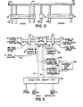
- a transfer bus 34 is represented, in the preferred embodiment employing multiple conductors, for example, a set of sixteen wires.
- the transfer bus 34 is treated as though it were a transmission line, but terminations do not exist in port or gate positions but only on the physical structure of the bus itself. Termination devices 90a and 90b are designed to ensure that signals carried on the transfer bus will make one transfer with no reflections.
- Input ports 20 and output ports 22 are shown as gates or ports of a substage matrix in the mid-stage. There is no apparent difference between input ports 20 and output ports 22. The difference is in the direction in which the signals travel. In the preferred embodiment, ten signals travel from input to output and six signals travel from output to input.
- the input ports 20 have circuitry to carry the input signals from ,external lines 92 through the ports 20 to the bus 34, while the output ports 22 have circuitry to carry those signals from the bus 34to lines 94. It is only this identification of signal direction which determines the difference between input and output ports.
- a monitor 32 carries all signals from the bus 34 to a monitor line 96b and acts as a bridge monitor to observe all sixteen of the signals in the preferred embodiment being carried on the transfer bus. Again, signal direction determines whether the port is labelled input, output or monitor.
- FIG. 3 an individual transfer bus matrix is schematically shown with its controls.
- a mid-substage is selected as generally representative.
- Each substrate shown or represented is provided by a transfer bus matrix in Figure 1 each functionally similar to all of the others with differing numbers of input and output ports.
- matrices of the first (F) and last (L) substages are the same size but a different size from those of the mid-substages (M), but their functions are identical. Only the count of input and output ports is different.
- a multiplex clock 36e creates a timing for an input control multiplex timing generator 36a which opens each of the input ports 20 in predetermined order via a control line 38.
- the input and output ports will be understood to be electronic gates or the equivalent.
- each input binary number is generated, it is examined by an output control multiplex timing generator 36b which compares it against the address which has been stored in a cross-connect memory unit 36d .
- the cross-connect memory unit 36d has inputs from an eight bit address bus, an eight bit steering bus, and a write strobe, all originating in an M stage control 68 (see Figure 1).
- the output control opens any output port which has stored in its memory an input number that matches the current input number. In this way, one or more (or none, if that is the case) of the output ports 22 are opened via a control line 39 at an input timing interval.
- the bridge monitor stored address (in cross-connect memory unit 36d) is also verified against the code generated for the input interval and, if it matches, a bridge monitor 32 opens and transfers the data unidirectionally from the bus 34 to a sixteen wire monitor 96 depicted in Figure 3.
- the sixteen wire monitor is specific to this particular preferred embodiment and could be designed to provide any number of signals of the transfer bus for the particular configuration for which it was built.
- the control information which produces the repetitive openings during the proper time slice is created in the control unit 68 (for the described stage). The information is supplied to all substages as an input address on the eight bit address bus and an output number, or the monitor identification, on the eight bit steering bus. These buses run to all the substages of a stage.
- the particular substage is identified by a unique wire emanating from the central M stage control 68 to the unique substage and is identified as the "write strobe".
- the write strobe identifies the substage that is to use the information that is on both buses. These control buses do not carry any signal data and do not operate at signal data speeds but operate only when changes in connections are desired.
- a fault clearing logic 36c is used to ensure that the buses remain clear.
- the fault clearing logic is required only on certain types of electronic component solutions to the transfer bus matrix not presently being used. It is intended for use after each input time interval to ensure that the buses do not contain any latched electronic equipment which might be burned off should a gate fail and remain connected. In that way, the particular gate could be physically burned out. Certain methods of implementation might require such a disposition of a fault to prevent losing a substage due to one bad set of gates. In the preferred embodiments tested to date, that mode of failure has not been calculated to be a high enough risk and such equipment has therefore been omitted.
- FIG. 1 shows the entire three stage transfer bus matrix and three monitor matrices 40a, 42 and 40b, which act to allow any throughput to be monitored.
- a preferred basic matrix arrangement is defined in the previously referred to 'European Patent Application. Utilizing the transfer bus substages in the three stage matrix, allows the monitoring of any throughput signals on hard wired interconnecting links 92 and 94, such that each substage has an output port to each substage of the successive stage.
- the port number of a substage matches the stage number of the successive stage; and the port number of the successive stage matches the substage number of the previous stage. That allows ease of identification in the preferred embodiment; but any number assignment can be used.
- Each individual substage is a transfer bus matrix.
- the first substage of the F stage, identified as 10a in Figure 1 contains, typically, all of theele- ments further defined in Figures 2 and 3, just as does each substage in the L stage and the M stage.
- the transfer bus 34 is shown with the bridge monitor 32 and is connected to the monitor transfer bus 40a.
- Input ports control 38 as well as output ports control 39 is provided.
- the input ports 16a through 16q of the respective F stage submatrices are similar to output ports 18a through 18q.
- the individual ports are identified by number, for example as input port 16a-1 through 16a-15.
- the output ports are shown as 18a-1 through 18a-15.
- Each port has many connections to the trasfer bus matrix as there are wires or channels and these individual wires may have designated signal directions.
- Input ports 20a through 20p, and 24a through 24q have similar connections with similar signal direction criteria existing in the M stage and . L stage respectively.
- the output ports 18a through 18q are similar to the output ports 22a through 22p and 26a through 26q, respectively.
- Figures 2 and 3 describe specifically the M stage matrices and describe gating functions of the input ports 20 and the output ports 22.
- Input ports 16 of the F stage and output ports 26 of the L stage in the illustrated three stage matrix embodiment do literally differ in that one or both sets typically contain level conversion equipment. That is, they handle signal levels to the Electronic Industries Association (EIA), specification No. RS-232 (Digital Communications).
- the ports are packaged slightly differently in terms of number of ports per printed circuit card in the different stages.
- the monitor lines which emanate from the bridge monitors 32 create all unidirectional signals travelling down the groups of lines 96a, 96b and 96c, respectively, toward the three monitor matrices 40a, 42 and 40b.
- the input ports of the three monitor matrices are controlled similarly to the other transfer bus substages. However, in the monitor transfer bus substages, all sixteen signals are unidirectional, that is, going from input port 46a to output port 58a, or from input port 46b towards output port 58b, or from input port 48 to output port 60. Similarly, the output ports 58a, 58b and 60 are unidirectional, taking data from the transfer bus to the outside lines.
- the bridge monitor 32 of the matrix substages allows stage controllers 66, 68 and 70 to monitor actual data flowing through the system based on information supplied by computer 72 and perform either reading of the data for control purposes, or monitoring of the data for evaluation of the throughput in terms of its integrity.
- transfer bus matrices regardless of whether they are in an F, M or L stage, or a monitor matrix, contain the same type of control, regardless of the size of the matrix.
- the count of input ports is set into the count of the input control multiplex timing generator 36a of Figure 3 and is used to limit the number of time slices for each substage activity.
- the monitor matrices allow the connection of any monitor line from any substage of the particular stage in question to reach a monitor interface output device 78 which allows the signal from one of the three monitor matrices to reach monitor test equipment ports 64a through 64j.
- Each of the three stage controllers 66, 68 and 70 is supplied with information by a computer 72, perhaps better described as a controller.
- the controller 72 selects the path from a desired input port 28 to a desired output port 30 via the desired M stage substage matrix. It does this in accordance with the rules found in the contemporaneously filed European Patent Application EP-A-0055944 or more specifically for the preferred three stage matrix ordinarily by the least used or first available M stage substage matrix that has paths available.
- This information is then passed to the controller 66, 68 and 70 to enable each stage to be individually controlled. However, for the sake of smoothness, in the preferred embodiment there are times when the commanding of the stages is done sequentially and other times when it is done simultaneously.
- a memory 74 retains a permanent record of the connections that have been made in chronological order while control consoles 76 permit manual or automatic inputs from which the desired external numbered connection requirements are provided.
- transfer bus matrix may be applied to individual substages or to an isolated matrix, or it may be applied to multistage matrices in which each of the stages has substage matrices in the form of transfer buses, as has been described.
- the invention has been described in broad terms and related to a specific embodiment. It will be understood by those skilled in the art that many modifications and variations of the systems described are possible within the scope of the following claims.
Landscapes
- Engineering & Computer Science (AREA)
- Computer Networks & Wireless Communication (AREA)
- Bus Control (AREA)
- Details Of Spanners, Wrenches, And Screw Drivers And Accessories (AREA)
- Logic Circuits (AREA)
- Electronic Switches (AREA)
- Use Of Switch Circuits For Exchanges And Methods Of Control Of Multiplex Exchanges (AREA)
- Multi Processors (AREA)
Claims (15)
Applications Claiming Priority (2)
| Application Number | Priority Date | Filing Date | Title |
|---|---|---|---|
| US06/222,064 US4393381A (en) | 1981-01-02 | 1981-01-02 | Transfer bus matrix |
| US222064 | 1981-01-02 |
Publications (2)
| Publication Number | Publication Date |
|---|---|
| EP0055943A1 EP0055943A1 (fr) | 1982-07-14 |
| EP0055943B1 true EP0055943B1 (fr) | 1986-03-12 |
Family
ID=22830654
Family Applications (1)
| Application Number | Title | Priority Date | Filing Date |
|---|---|---|---|
| EP81306191A Expired EP0055943B1 (fr) | 1981-01-02 | 1981-12-31 | Système de commutation à matrices comprenant un bus de transfert |
Country Status (5)
| Country | Link |
|---|---|
| US (1) | US4393381A (fr) |
| EP (1) | EP0055943B1 (fr) |
| JP (1) | JPS57141195A (fr) |
| CA (1) | CA1173143A (fr) |
| DE (1) | DE3174115D1 (fr) |
Families Citing this family (17)
| Publication number | Priority date | Publication date | Assignee | Title |
|---|---|---|---|---|
| US4491838A (en) * | 1982-07-28 | 1985-01-01 | International Business Machines Corporation | Starloop communication network and control system therefor |
| US4683564A (en) * | 1982-11-22 | 1987-07-28 | Data Switch Corporation | Matrix switch system |
| US4630045A (en) * | 1983-10-24 | 1986-12-16 | International Business Machines Corporation | Controller for a cross-point switching matrix |
| US4605928A (en) * | 1983-10-24 | 1986-08-12 | International Business Machines Corporation | Fault-tolerant array of cross-point switching matrices |
| US4633245A (en) * | 1983-12-30 | 1986-12-30 | International Business Machines Corporation | Local area network interconnect switching system |
| US4752777A (en) * | 1985-03-18 | 1988-06-21 | International Business Machines Corporation | Delta network of a cross-point switch |
| JPS61214694A (ja) * | 1985-03-18 | 1986-09-24 | インタ−ナショナル ビジネス マシ−ンズ コ−ポレ−ション | データ伝送のスイッチング装置 |
| US4725835A (en) * | 1985-09-13 | 1988-02-16 | T-Bar Incorporated | Time multiplexed bus matrix switching system |
| US4858228A (en) * | 1987-02-16 | 1989-08-15 | Ricoh Company, Ltd. | Communication system employing multi-conjunction architecture |
| JPH0191556A (ja) * | 1987-03-20 | 1989-04-11 | Ricoh Co Ltd | 不定形通信網のノ−ド装置 |
| JPS63276940A (ja) * | 1987-03-26 | 1988-11-15 | Ricoh Co Ltd | 不定形通信網のノ−ド装置 |
| US4928022A (en) * | 1987-07-17 | 1990-05-22 | Trw Inc. | Redundancy interconnection circuitry |
| JPH01175413A (ja) * | 1987-12-29 | 1989-07-11 | Matsushita Electric Ind Co Ltd | ディジタル装置 |
| US5282195A (en) * | 1991-09-05 | 1994-01-25 | Raynet Corporation | DSO cross-connect for floating virtual tributaries |
| US5809221A (en) * | 1995-06-07 | 1998-09-15 | Cornet, Inc. | Apparatus and method for detecting and bypassing faulty switches in a digital matrix switch |
| US6816486B1 (en) | 1999-03-25 | 2004-11-09 | Inrange Technologies Corporation | Cross-midplane switch topology |
| JP4904497B2 (ja) * | 2006-12-25 | 2012-03-28 | 国立大学法人秋田大学 | 多段スイッチの制御回路 |
Citations (1)
| Publication number | Priority date | Publication date | Assignee | Title |
|---|---|---|---|---|
| EP0005220A2 (fr) * | 1978-04-29 | 1979-11-14 | Telefonbau und Normalzeit GmbH | Montage pour centraux de télécommunication à multiplexage temporel de signaux numériques, en particulier des centraux téléphoniques |
Family Cites Families (9)
| Publication number | Priority date | Publication date | Assignee | Title |
|---|---|---|---|---|
| DE2211400C2 (de) * | 1972-03-09 | 1974-02-21 | Telefonbau Und Normalzeit Gmbh, 6000 Frankfurt | Zweistufiges Zeitmultiplex-Vermittlungssystem |
| US3892925A (en) * | 1974-06-03 | 1975-07-01 | Ibm | Electric signal exchange switching arrangement |
| US3959594A (en) * | 1974-07-01 | 1976-05-25 | Gte Automatic Electric Laboratories Incorporated | Arrangement and method for the localized self-control of randomly allotted time slots to audio ports |
| US4201891A (en) * | 1978-03-17 | 1980-05-06 | International Telephone And Telegraph Corporation | Expandable digital switching network |
| JPS5428516A (en) * | 1977-08-08 | 1979-03-03 | Nippon Telegr & Teleph Corp <Ntt> | Channel converter |
| US4138597A (en) * | 1977-09-06 | 1979-02-06 | International Telephone And Telegraph Corporation | PCM time slot exchange |
| JPS5810021B2 (ja) * | 1978-05-24 | 1983-02-23 | 富士通株式会社 | 時分割多重ネツトワ−ク・システム |
| JPS5853838B2 (ja) * | 1978-08-04 | 1983-12-01 | 日本電信電話株式会社 | 時分割通話路装置 |
| US4251880A (en) * | 1979-07-31 | 1981-02-17 | Bell Telephone Laboratories, Incorporated | Digital loop switch for controlling data information having differing transmission characteristics |
-
1981
- 1981-01-02 US US06/222,064 patent/US4393381A/en not_active Expired - Fee Related
- 1981-12-28 JP JP56210134A patent/JPS57141195A/ja active Pending
- 1981-12-31 EP EP81306191A patent/EP0055943B1/fr not_active Expired
- 1981-12-31 CA CA000393483A patent/CA1173143A/fr not_active Expired
- 1981-12-31 DE DE8181306191T patent/DE3174115D1/de not_active Expired
Patent Citations (1)
| Publication number | Priority date | Publication date | Assignee | Title |
|---|---|---|---|---|
| EP0005220A2 (fr) * | 1978-04-29 | 1979-11-14 | Telefonbau und Normalzeit GmbH | Montage pour centraux de télécommunication à multiplexage temporel de signaux numériques, en particulier des centraux téléphoniques |
Also Published As
| Publication number | Publication date |
|---|---|
| US4393381A (en) | 1983-07-12 |
| EP0055943A1 (fr) | 1982-07-14 |
| CA1173143A (fr) | 1984-08-21 |
| DE3174115D1 (en) | 1986-04-17 |
| JPS57141195A (en) | 1982-09-01 |
Similar Documents
| Publication | Publication Date | Title |
|---|---|---|
| US4393381A (en) | Transfer bus matrix | |
| US4683550A (en) | Personal computer instrumentation system including carrier board having bus-oriented plug-in instrumentation modules | |
| US3924240A (en) | System for controlling processing equipment | |
| CA2061599A1 (fr) | Systeme de commande programmable | |
| JPH07262128A (ja) | 直列のマスター・スレーブ装置において機能ユニットを構成する方法と装置 | |
| EP0282267A3 (fr) | Interface de réseau adaptatif numérique | |
| EP0190679A2 (fr) | Système de commutation de canaux temporels téléphoniques centralisé avec image sensible à l'état du réseau | |
| CA1203876A (fr) | Unite de controle peripherique pour systeme telephonique numerique | |
| US4217658A (en) | Process control system that controls its outputs according to the results of successive analysis of the vertical input columns of a hypothetical ladder diagram | |
| EP0378122A1 (fr) | Matrice de commutation temporelle parallèle et module commutateur pour être appliqué dans cette matrice | |
| EP0042666B1 (fr) | Module de commutation numérique pour télécommunication à multiplexage temporel | |
| KR100232980B1 (ko) | 광 스위칭 매트릭스 | |
| EP0347929A3 (fr) | Processeurs à traitement parallèle | |
| US4719562A (en) | Multiprocessor system for intercommunication of processors | |
| US3281537A (en) | Multiplex switching stage and its associated control circuits | |
| US6301623B1 (en) | Computer network with a plurality of identically addressed devices | |
| US4138597A (en) | PCM time slot exchange | |
| US4220824A (en) | Interface linking synchronous sense and drive matrices of telephone system with a processor of signalization data | |
| US4942573A (en) | Loosely coupled parallel network simulator | |
| US3809819A (en) | Tdm switching apparatus | |
| CA1260166A (fr) | Repartiteur de voies de communication numeriques | |
| RU2071635C1 (ru) | Цифровой регулятор для многодвигательного электропривода | |
| ATE136718T1 (de) | Schaltungsanordnung für eine zentralgesteuerte fernmeldevermittlungsanlage, insbesondere pcm- fernsprechvermittlungsanlage, mit zentralem koordinationsprozessor und dezentralen anschlussgruppen mit teilsteuerwerken | |
| JPH0118463B2 (fr) | ||
| SU1297069A1 (ru) | Устройство дл сопр жени внешних устройств с общей пам тью |
Legal Events
| Date | Code | Title | Description |
|---|---|---|---|
| PUAI | Public reference made under article 153(3) epc to a published international application that has entered the european phase |
Free format text: ORIGINAL CODE: 0009012 |
|
| AK | Designated contracting states |
Designated state(s): BE CH DE FR GB IT NL SE |
|
| 17P | Request for examination filed |
Effective date: 19830111 |
|
| GRAA | (expected) grant |
Free format text: ORIGINAL CODE: 0009210 |
|
| AK | Designated contracting states |
Kind code of ref document: B1 Designated state(s): BE CH DE FR GB IT LI NL SE |
|
| ITF | It: translation for a ep patent filed | ||
| REF | Corresponds to: |
Ref document number: 3174115 Country of ref document: DE Date of ref document: 19860417 |
|
| ET | Fr: translation filed | ||
| PGFP | Annual fee paid to national office [announced via postgrant information from national office to epo] |
Ref country code: NL Payment date: 19861231 Year of fee payment: 6 |
|
| PLBE | No opposition filed within time limit |
Free format text: ORIGINAL CODE: 0009261 |
|
| STAA | Information on the status of an ep patent application or granted ep patent |
Free format text: STATUS: NO OPPOSITION FILED WITHIN TIME LIMIT |
|
| 26N | No opposition filed | ||
| PG25 | Lapsed in a contracting state [announced via postgrant information from national office to epo] |
Ref country code: LI Effective date: 19871231 Ref country code: CH Effective date: 19871231 Ref country code: BE Effective date: 19871231 |
|
| PG25 | Lapsed in a contracting state [announced via postgrant information from national office to epo] |
Ref country code: SE Effective date: 19880101 |
|
| BERE | Be: lapsed |
Owner name: T-BAR INC. Effective date: 19871231 |
|
| PG25 | Lapsed in a contracting state [announced via postgrant information from national office to epo] |
Ref country code: NL Effective date: 19880701 |
|
| NLV4 | Nl: lapsed or anulled due to non-payment of the annual fee | ||
| GBPC | Gb: european patent ceased through non-payment of renewal fee | ||
| PG25 | Lapsed in a contracting state [announced via postgrant information from national office to epo] |
Ref country code: FR Free format text: LAPSE BECAUSE OF NON-PAYMENT OF DUE FEES Effective date: 19880831 |
|
| REG | Reference to a national code |
Ref country code: CH Ref legal event code: PL |
|
| PG25 | Lapsed in a contracting state [announced via postgrant information from national office to epo] |
Ref country code: DE Effective date: 19880901 |
|
| REG | Reference to a national code |
Ref country code: FR Ref legal event code: ST |
|
| PG25 | Lapsed in a contracting state [announced via postgrant information from national office to epo] |
Ref country code: GB Free format text: LAPSE BECAUSE OF NON-PAYMENT OF DUE FEES Effective date: 19881121 |
|
| EUG | Se: european patent has lapsed |
Ref document number: 81306191.8 Effective date: 19880913 |