EP0058548A1 - Procédé de fabrication d'un dispositif semiconducteur du type MOSFET - Google Patents
Procédé de fabrication d'un dispositif semiconducteur du type MOSFET Download PDFInfo
- Publication number
- EP0058548A1 EP0058548A1 EP82300741A EP82300741A EP0058548A1 EP 0058548 A1 EP0058548 A1 EP 0058548A1 EP 82300741 A EP82300741 A EP 82300741A EP 82300741 A EP82300741 A EP 82300741A EP 0058548 A1 EP0058548 A1 EP 0058548A1
- Authority
- EP
- European Patent Office
- Prior art keywords
- gate electrode
- insulating layer
- aluminum
- layer
- gate
- Prior art date
- Legal status (The legal status is an assumption and is not a legal conclusion. Google has not performed a legal analysis and makes no representation as to the accuracy of the status listed.)
- Granted
Links
Images


Classifications
-
- H—ELECTRICITY
- H10—SEMICONDUCTOR DEVICES; ELECTRIC SOLID-STATE DEVICES NOT OTHERWISE PROVIDED FOR
- H10B—ELECTRONIC MEMORY DEVICES
- H10B12/00—Dynamic random access memory [DRAM] devices
- H10B12/30—DRAM devices comprising one-transistor - one-capacitor [1T-1C] memory cells
-
- H—ELECTRICITY
- H10—SEMICONDUCTOR DEVICES; ELECTRIC SOLID-STATE DEVICES NOT OTHERWISE PROVIDED FOR
- H10D—INORGANIC ELECTRIC SEMICONDUCTOR DEVICES
- H10D64/00—Electrodes of devices having potential barriers
- H10D64/60—Electrodes characterised by their materials
- H10D64/66—Electrodes having a conductor capacitively coupled to a semiconductor by an insulator, e.g. MIS electrodes
- H10D64/665—Electrodes having a conductor capacitively coupled to a semiconductor by an insulator, e.g. MIS electrodes the conductor comprising a layer of elemental metal contacting the insulator, e.g. tungsten or molybdenum
-
- H—ELECTRICITY
- H10—SEMICONDUCTOR DEVICES; ELECTRIC SOLID-STATE DEVICES NOT OTHERWISE PROVIDED FOR
- H10P—GENERIC PROCESSES OR APPARATUS FOR THE MANUFACTURE OR TREATMENT OF DEVICES COVERED BY CLASS H10
- H10P34/00—Irradiation with electromagnetic or particle radiation of wafers, substrates or parts of devices
- H10P34/40—Irradiation with electromagnetic or particle radiation of wafers, substrates or parts of devices with high-energy radiation
- H10P34/42—Irradiation with electromagnetic or particle radiation of wafers, substrates or parts of devices with high-energy radiation with electromagnetic radiation, e.g. laser annealing
-
- Y—GENERAL TAGGING OF NEW TECHNOLOGICAL DEVELOPMENTS; GENERAL TAGGING OF CROSS-SECTIONAL TECHNOLOGIES SPANNING OVER SEVERAL SECTIONS OF THE IPC; TECHNICAL SUBJECTS COVERED BY FORMER USPC CROSS-REFERENCE ART COLLECTIONS [XRACs] AND DIGESTS
- Y10—TECHNICAL SUBJECTS COVERED BY FORMER USPC
- Y10S—TECHNICAL SUBJECTS COVERED BY FORMER USPC CROSS-REFERENCE ART COLLECTIONS [XRACs] AND DIGESTS
- Y10S148/00—Metal treatment
- Y10S148/09—Laser anneal
-
- Y—GENERAL TAGGING OF NEW TECHNOLOGICAL DEVELOPMENTS; GENERAL TAGGING OF CROSS-SECTIONAL TECHNOLOGIES SPANNING OVER SEVERAL SECTIONS OF THE IPC; TECHNICAL SUBJECTS COVERED BY FORMER USPC CROSS-REFERENCE ART COLLECTIONS [XRACs] AND DIGESTS
- Y10—TECHNICAL SUBJECTS COVERED BY FORMER USPC
- Y10S—TECHNICAL SUBJECTS COVERED BY FORMER USPC CROSS-REFERENCE ART COLLECTIONS [XRACs] AND DIGESTS
- Y10S148/00—Metal treatment
- Y10S148/091—Laser beam processing of fets
-
- Y—GENERAL TAGGING OF NEW TECHNOLOGICAL DEVELOPMENTS; GENERAL TAGGING OF CROSS-SECTIONAL TECHNOLOGIES SPANNING OVER SEVERAL SECTIONS OF THE IPC; TECHNICAL SUBJECTS COVERED BY FORMER USPC CROSS-REFERENCE ART COLLECTIONS [XRACs] AND DIGESTS
- Y10—TECHNICAL SUBJECTS COVERED BY FORMER USPC
- Y10S—TECHNICAL SUBJECTS COVERED BY FORMER USPC CROSS-REFERENCE ART COLLECTIONS [XRACs] AND DIGESTS
- Y10S148/00—Metal treatment
- Y10S148/141—Self-alignment coat gate
Definitions
- This invention relates to a method of producing a metal oxide semiconductor field effect transistor (MOS FET).
- the method may be applied to the formation of a semiconductor memory device comprising an MOS transistor and a capacitor (i.e. a so-called “one-transistor one-capacitor memory cell").
- a gate electrode of an MOS transistor is often made of polycrystalline silicon.
- a thin gate insulating layer e.g. a silicon dioxide layer
- a semiconductor substrate e.g. a silicon wafer
- a polycrystalline silicon layer is formed on the gate insulating layer by a chemical vapour deposition (CVD) method.
- a photoresist layer is formed on the polycrystalline silicon layer, exposed through a photomask, and developed.
- the polycrystalline silicon layer and the gate insulating layer are selectively etched, using the photoresist layer as a mask, to form the polycrystalline silicon gate electrode.
- Impurities e.g. boron or phosphorus
- the impurities are introduced by an ion-implantation method, it is necessary to anneal the doped regions (i.e. the source and drain regions) at an elevated temperature for activation of the introduced impurities and for repairing the crystalline damage.
- the impurities are introduced by a thermal diffusion method, the semiconductor substrate is heated to an elevated temperature during the diffusion of the impurities. Such an elevated temperature does not affect the polycrystalline silicon gate. Furthermore, it is possible to form easily an insulating layer covering the polycrystalline silicon gate by thermally oxidizing the polycrystalline silicon gate.
- An MOS transistor having a polycrystalline silicon gate can, for example, be utilised to form a one-transistor one-capacitor memory cell (see V.Leo Rideout, One-Device Cells for Dynamic Random-Access Memories, IEEE Transactions on Electron Devices, Vol.ED-26, No.6, PP.839-852, June 1979).
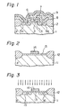
- Fig.1 of the accompanying drawings shows a cross- section through one example of the various known structures of one-transistor one-capacitor memory cells.
- the memory device of Fig.1 comprises a p-type silicon semiconductor substrate 1, a field insulating layer (e.g. a thick silicon dioxide layer) 2, a gate insulating layer (e.g. a thin silicon dioxide layer) 3, a polycrystalline silicon gate electrode 4, n -type doped regions 5a and 5b which are formed by introducing n-type impurities into the semiconductor substrate 1 in a self-alignment manner using the gate electrode 4 as a mask, an insulating layer 6 (e.g.
- the polycrystalline silicon gate electrode 4 serves as a word line
- the conductive line 9 serves as a bit line.
- the capacitor plate 7 is connected to a power source line (V DD ) '
- the heavily-doped polycrystalline silicon of the gate electrode has a resistivity of 1-2 x 10 -3 ⁇ cm (ohm centimetre), which limits the switching speed of the MOS transistor. If the gate electrode is made of aluminum having a resistivity of 1-2 x 10 -6 ⁇ cm, the switching speed can be increased. However, since the melting point of aluminum is 629°C and aluminum alloys with silicon around 500°C, a semiconductor device having an aluminum layer should not be heated to a temperature of more than about 500 o C. Therefore, in the fabrication of aluminum gate MOS transistors, aluminum gate electrodes are usually formed after the formation of source and drain regions. In this case, source and drain regions are not self-aligned to the gate electrode and the mask-to-mask misregistration tolerance should be taken in consideration. Accordingly, one cannot sufficiently increase the density of the semiconductor device.
- An object of the present invention is to provide a method of producing an MOS transistor having a high switching speed and a high density.
- a method of producing a semiconductor device which comprises a metal oxide semiconductor field effect transistor, comprising the steps of: forming a gate electrode on a gate insulating layer lying on a semiconductor substrate; introducing impurities into the semiconductor substrate to form at least one doped region by an ion-implantation method using the gate electrode as a mask; and annealing the doped region, characterised in that the gate electrode is made of aluminum and that the annealing step is carried out by irradiation by a laser beam.
- An n-channel MOS transistor is produced in accordance with the method of the present invention in the following manner.
- a p-type silicon semiconductor substrate 11 (Fig. 2) is selectively oxidized by a conventional thermal oxidation method using a silicon nitrode layer mask (not shown) to form a field insulating layer 12 of silicon dioxide.
- the thickness of the field insulating layer 12 is, for example, approximately 800nm.
- the silicon substrate 11 is oxidized by the conventional thermal oxidation method to form a gate insulating layer 13 (Fig. 2) of silicon dioxide.
- the thickness of the gate insulating layer 13 is, for example, approximately 40nm.
- an aluminum layer having a thickness of, for example, 500nm is formed on the gate insulating layer 13 and on the field insulating layer 12 by a conventional vapor deposition method.
- the aluminum layer is selectively removed by a photoetching method to form a gate electrode 14 (Fig. 2).
- Donor (n-type) impurities e.g. arsenic, phosphorus
- n + -type doped regions i.e. a drain region and a source region 15 and 16, as illustrated in Fig. 3.
- arsenic ions are implanted at an implant energy of 150 KeV with a dose of 4 x 10 cm .
- the field insulating layer 12 and the aluminum gate electrode 14 do not permit passage of the impurities through them, namely they serve as masks.
- a laser beam is irradiated to the obtained device to anneal the n + -type doped regions 15 and 16. Namely, laser annealing is carried out.
- the aluminum gate electrode 14 absorbs only a part of the laser beam and the gate electrode 14 is not heated to an elevated temperature.
- the n +- type doped regions 15 and 16 absorb the laser beam well so as to anneal themselves.
- a laser beam having a wavelength of 0.9 ⁇ m or more taking the absorption factor of aluminum into consideration.
- the absorption curve of aluminum is indicated with a solid line in Fig. 4.
- a laser not significantly heating aluminum should be used for the laser annealing. For example, if one were to use a ruby laser having a wavelength of 0.6943 pm and irradiate at an energy density of 1.16 J/cm 2 , the sheet resistance of the n + -type doped regions 15 and 16 would reduce to only 300 ohm/square ( ⁇ / ⁇ ). This sheet resistance value would be too large.
- the sheet resistance would be reduced to 30 ohm/square.
- a network of cracks would be formed at the surface of the aluminum gate electrode 14.
- Nd:YAG lasers As a laser having a wavelength of 0.9 U m or more, there are Nd:YAG lasers, C0 2 lasers etc.
- an antireflection coating on only the doped regions. For example, if a silicon dioxide layer having a thickness of 180 nm is formed on the doped region of the silicon substrate as the antireflection coating for the Nd:YAG laser, the intensity of the absorbed beam in the silicon is 95% of the intensity of irradiation of the laser beam. In this case, the efficiency of the laser annealing is also increased and the sheet resistance of the doped region is reduced to 20 ohm/square.
- an insulating layer 17 of, for example, phosphosilicate glass (PSG) is formed by a conventional chemical vapor deposition (CVD) method, as illustrated in Fig. 5.
- the insulating layer 17 and the gate insulating layer 13 are selectively etched by a photoetching method to form contact holes on the n -type doped regions 15 and 16 and on the gate electrode 14.
- a conductive layer of, for example, aluminum is formed on the insulating layer 17 by a vapor deposition method and is patterned by a photoetchi n g method to form interconnection lines for drain, gate and source 18a, 18b and 18c.
- an N channel type MOS transistor is produced.
- a semiconductor memory cell comprising an MOS transistor and a capacitor and having a similar structure to that illustrated in Fig. 1 is produced in accordance with the method of the present invention in the following manner.
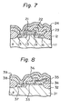
- the aluminum gate electrode (i.e., a word line) 14 is oxidized at a temperature of up to 500°C to form an aluminum oxide (A1 2 0 3 ) layer 21 having a thickness of, for example, approximately 100 nm, as illustrated in F ig. 6.
- the aluminum oxide layer 21 serves as a good insulator and is formed by a plasma oxidation method, a wet anodizing method, a DC plasma anodization method, or dipping in warm water having a temperature of approximately 60°C.
- another aluminum layer having a thickness of, for example, 500 nm is formed on the aluminum oxide layer 21, the gate insulating layer 13, and the field insulating layer 12 by a vapor deposition method.
- the aluminum layer is selectively removed by a photoetching method to form a capacitor plate 22, as illustrated in Fig. 7.
- An insulating layer 23 (Fig. 7) of, for example, PSG is formed by a CVD method on the entire surface of the obtained device.
- the thickness of the insulating layer 23 is, for example, 500 nm.
- the insulating layer 23 and the gate insulating layer 13 are selectively etched by a photoetching method to form a contact hole on the n +- type doped region 15.
- a conductive layer of, for example, aluminum is formed on the insulating layer 23 by a vapor deposition method and is patterned by a photoetching method to form a conductive line (i.e., a bit line) contacting with the n -type doped region 15 through the contact hole, as illustrated in Fig. 7.
- the resultant one-transistor one-capacitor memory cell has a bit line and word line made of aluminum, so the switching speed of the memory cell is high. Furthermore, the doped regions (i.e., the drain and source regions of the M OS transistor) are formed in a self-alignment manner, so the area of the memory cell is small, namely, the density of a dynamic random access memory (RAM) integrated circuit comprising a large number of the memory cells is high.
- RAM dynamic random access memory
- Another type of semiconductor memory cell comprising an MOS .transistor and a capacitor, being illustrated in F ig. 8, is produced in accordance with the method of the present invention in the following manner.
- a p-type silicon semiconductor substrate 31 is selectively oxidized by a thermal oxidation method to form a field insulating (silicon dioxide) layer 32. Then, the portion of the silicon substrate which is not covered with the field oxide layer 32 is thermally oxidized to form a gate insulating (silicon dioxide) layer 33 in the same manner as in Embodiment 1.
- An aluminum layer is formed on the oxide layer 32 and the gate oxide layer 33 by a vapor deposition method and is selectively etched by a photoetching method to form a capacitor plate 34.
- the aluminum capacitor plate 34 is oxidized by, for example, a plasma oxidation method to form an aluminum oxide layer 35 thereon. It is possible to make the capacitor plate of polycrystalline silicon instead of aluminum.
- Another aluminum layer is then formed on the entire surface of the obtained memory cell by a vapor deposition method and is selectively etched by a photoetching method to form a gate electrode 36 (i.e., a word line).
- Donor impurities e.g., arsenic
- the field oxide layer 32, the capacitor plate 34, and the gate electrode 36 serve as masks preventing the impurities from passing therethrough.
- the n +- type doped region 37 is self-aligned to the gate electrode 36.
- the laser annealing for the n +- type doped region 37 is carried out by irradiation of a laser beam in the same manner as that of Embodiment 1.
- An insulating layer 38 of PSG then is formed on the entire surface of the obtained memory cell by a CVD method.
- the insulating layer 38 and the gate oxide layer 33 are selectively etched by a photoetching method to form a contact hole on the doped region.
- an aluminum layer is formed on the insulating layer 38 by a vapor deposition method and is patterned by a photoetching method to form a conductor line 39 (i.e., a bit line) connecting to the n +- type doped region 37 through the contact hole, as illustrated in Fig. 8.
- the resultant memory cell does not have a doped region under the capacitor plate 34, but an inversion layer occurs in the silicon substrate 31 under the capacitor plate 34 if an appropriate bias is applied to the capacitor plate 34.
Landscapes
- Semiconductor Memories (AREA)
Applications Claiming Priority (4)
| Application Number | Priority Date | Filing Date | Title |
|---|---|---|---|
| JP56021296A JPS57134963A (en) | 1981-02-16 | 1981-02-16 | Semiconductor memory |
| JP21296/81 | 1981-02-16 | ||
| JP22393/81 | 1981-02-18 | ||
| JP56022393A JPS57136372A (en) | 1981-02-18 | 1981-02-18 | Manufacture of mos type field effect semiconductor device |
Publications (2)
| Publication Number | Publication Date |
|---|---|
| EP0058548A1 true EP0058548A1 (fr) | 1982-08-25 |
| EP0058548B1 EP0058548B1 (fr) | 1986-08-06 |
Family
ID=26358334
Family Applications (1)
| Application Number | Title | Priority Date | Filing Date |
|---|---|---|---|
| EP82300741A Expired EP0058548B1 (fr) | 1981-02-16 | 1982-02-15 | Procédé de fabrication d'un dispositif semiconducteur du type MOSFET |
Country Status (3)
| Country | Link |
|---|---|
| US (1) | US4646426A (fr) |
| EP (1) | EP0058548B1 (fr) |
| DE (1) | DE3272410D1 (fr) |
Families Citing this family (42)
| Publication number | Priority date | Publication date | Assignee | Title |
|---|---|---|---|---|
| JPS6116571A (ja) * | 1984-07-03 | 1986-01-24 | Ricoh Co Ltd | 半導体装置の製造方法 |
| JPH0789569B2 (ja) * | 1986-03-26 | 1995-09-27 | 株式会社日立製作所 | 半導体集積回路装置及びその製造方法 |
| US4855252A (en) * | 1988-08-22 | 1989-08-08 | International Business Machines Corporation | Process for making self-aligned contacts |
| US5289030A (en) | 1991-03-06 | 1994-02-22 | Semiconductor Energy Laboratory Co., Ltd. | Semiconductor device with oxide layer |
| US5521107A (en) * | 1991-02-16 | 1996-05-28 | Semiconductor Energy Laboratory Co., Ltd. | Method for forming a field-effect transistor including anodic oxidation of the gate |
| EP0499979A3 (en) | 1991-02-16 | 1993-06-09 | Semiconductor Energy Laboratory Co., Ltd. | Electro-optical device |
| JP2794678B2 (ja) * | 1991-08-26 | 1998-09-10 | 株式会社 半導体エネルギー研究所 | 絶縁ゲイト型半導体装置およびその作製方法 |
| USRE36314E (en) * | 1991-03-06 | 1999-09-28 | Semiconductor Energy Laboratory Co., Ltd. | Insulated gate field effect semiconductor devices having a LDD region and an anodic oxide film of a gate electrode |
| US6713783B1 (en) * | 1991-03-15 | 2004-03-30 | Semiconductor Energy Laboratory Co., Ltd. | Compensating electro-optical device including thin film transistors |
| JP2873632B2 (ja) | 1991-03-15 | 1999-03-24 | 株式会社半導体エネルギー研究所 | 半導体装置 |
| JP2794499B2 (ja) * | 1991-03-26 | 1998-09-03 | 株式会社半導体エネルギー研究所 | 半導体装置の作製方法 |
| US6778231B1 (en) | 1991-06-14 | 2004-08-17 | Semiconductor Energy Laboratory Co., Ltd. | Electro-optical display device |
| US5414442A (en) * | 1991-06-14 | 1995-05-09 | Semiconductor Energy Laboratory Co., Ltd. | Electro-optical device and method of driving the same |
| US6975296B1 (en) | 1991-06-14 | 2005-12-13 | Semiconductor Energy Laboratory Co., Ltd. | Electro-optical device and method of driving the same |
| JP2845303B2 (ja) | 1991-08-23 | 1999-01-13 | 株式会社 半導体エネルギー研究所 | 半導体装置とその作製方法 |
| US5434742A (en) * | 1991-12-25 | 1995-07-18 | Hitachi, Ltd. | Capacitor for semiconductor integrated circuit and method of manufacturing the same |
| US5485019A (en) | 1992-02-05 | 1996-01-16 | Semiconductor Energy Laboratory Co., Ltd. | Semiconductor device and method for forming the same |
| US6624450B1 (en) | 1992-03-27 | 2003-09-23 | Semiconductor Energy Laboratory Co., Ltd. | Semiconductor device and method for forming the same |
| JP2905032B2 (ja) * | 1992-05-12 | 1999-06-14 | シャープ株式会社 | 金属配線の製造方法 |
| JP3211377B2 (ja) * | 1992-06-17 | 2001-09-25 | ソニー株式会社 | 半導体装置の製造方法 |
| JPH06124913A (ja) | 1992-06-26 | 1994-05-06 | Semiconductor Energy Lab Co Ltd | レーザー処理方法 |
| JP3211394B2 (ja) * | 1992-08-13 | 2001-09-25 | ソニー株式会社 | 半導体装置の製造方法 |
| US6624477B1 (en) | 1992-10-09 | 2003-09-23 | Semiconductor Energy Laboratory Co., Ltd. | Semiconductor device and method for manufacturing the same |
| TW232751B (en) | 1992-10-09 | 1994-10-21 | Semiconductor Energy Res Co Ltd | Semiconductor device and method for forming the same |
| KR940018962A (ko) * | 1993-01-29 | 1994-08-19 | 이헌조 | 알루미나를 이용한 수직형 박막 트랜지스터 제조방법 |
| JPH06232069A (ja) * | 1993-02-04 | 1994-08-19 | Semiconductor Energy Lab Co Ltd | 半導体装置の作製方法 |
| JP3562588B2 (ja) | 1993-02-15 | 2004-09-08 | 株式会社半導体エネルギー研究所 | 半導体装置の製造方法 |
| JPH0730125A (ja) * | 1993-07-07 | 1995-01-31 | Semiconductor Energy Lab Co Ltd | 半導体装置およびその作製方法 |
| TW297142B (fr) | 1993-09-20 | 1997-02-01 | Handotai Energy Kenkyusho Kk | |
| US5576231A (en) * | 1993-11-05 | 1996-11-19 | Semiconductor Energy Laboratory Co., Ltd. | Process for fabricating an insulated gate field effect transistor with an anodic oxidized gate electrode |
| US5614421A (en) * | 1994-03-11 | 1997-03-25 | United Microelectronics Corp. | Method of fabricating junction termination extension structure for high-voltage diode devices |
| US5401682A (en) * | 1994-03-11 | 1995-03-28 | United Microelectronics Corp. | Method of fabricating high voltage junction termination extension structure for a semiconductor integrated circuit device |
| JP3402400B2 (ja) | 1994-04-22 | 2003-05-06 | 株式会社半導体エネルギー研究所 | 半導体集積回路の作製方法 |
| US6747627B1 (en) | 1994-04-22 | 2004-06-08 | Semiconductor Energy Laboratory Co., Ltd. | Redundancy shift register circuit for driver circuit in active matrix type liquid crystal display device |
| JP3330736B2 (ja) * | 1994-07-14 | 2002-09-30 | 株式会社半導体エネルギー研究所 | 半導体装置の作製方法 |
| US6221726B1 (en) * | 1995-10-26 | 2001-04-24 | The Regents Of The University Of Claifornia | Process for fabricating device structures for real-time process control of silicon doping |
| US6372592B1 (en) * | 1996-12-18 | 2002-04-16 | United States Of America As Represented By The Secretary Of The Navy | Self-aligned MOSFET with electrically active mask |
| US6451644B1 (en) * | 1998-11-06 | 2002-09-17 | Advanced Micro Devices, Inc. | Method of providing a gate conductor with high dopant activation |
| US6370502B1 (en) * | 1999-05-27 | 2002-04-09 | America Online, Inc. | Method and system for reduction of quantization-induced block-discontinuities and general purpose audio codec |
| US6551888B1 (en) * | 2001-12-18 | 2003-04-22 | Advanced Micro Devices, Inc. | Tuning absorption levels during laser thermal annealing |
| US20070092998A1 (en) * | 2005-10-20 | 2007-04-26 | Ruey-Feng Tai | Semiconductor heat-transfer method |
| US8779515B2 (en) | 2012-05-21 | 2014-07-15 | International Business Machines Corporation | Semiconductor structure containing an aluminum-containing replacement gate electrode |
Citations (4)
| Publication number | Priority date | Publication date | Assignee | Title |
|---|---|---|---|---|
| DE2344513A1 (de) * | 1973-09-04 | 1975-03-27 | Siemens Ag | Ein-transistor-speicherelement |
| DE2705444A1 (de) * | 1977-02-09 | 1978-08-10 | Siemens Ag | Verfahren zur lokal begrenzten erwaermung eines festkoerpers |
| DE2837653A1 (de) * | 1978-08-29 | 1980-04-17 | Siemens Ag | Verfahren zur lokal begrenzten erwaermung von festkoerpern |
| US4243433A (en) * | 1978-01-18 | 1981-01-06 | Gibbons James F | Forming controlled inset regions by ion implantation and laser bombardment |
Family Cites Families (7)
| Publication number | Priority date | Publication date | Assignee | Title |
|---|---|---|---|---|
| US3514844A (en) * | 1967-12-26 | 1970-06-02 | Hughes Aircraft Co | Method of making field-effect device with insulated gate |
| US3808472A (en) * | 1972-12-29 | 1974-04-30 | Gen Electric | Variable capacitance semiconductor devices |
| JPS583380B2 (ja) * | 1977-03-04 | 1983-01-21 | 株式会社日立製作所 | 半導体装置とその製造方法 |
| US4274193A (en) * | 1979-07-05 | 1981-06-23 | Rca Corporation | Method for making a closed gate MOS transistor with self-aligned contacts |
| US4366613A (en) * | 1980-12-17 | 1983-01-04 | Ibm Corporation | Method of fabricating an MOS dynamic RAM with lightly doped drain |
| JPS5823479A (ja) * | 1981-08-05 | 1983-02-12 | Fujitsu Ltd | 半導体装置の製造方法 |
| US4441249A (en) * | 1982-05-26 | 1984-04-10 | Bell Telephone Laboratories, Incorporated | Semiconductor integrated circuit capacitor |
-
1982
- 1982-02-15 DE DE8282300741T patent/DE3272410D1/de not_active Expired
- 1982-02-15 EP EP82300741A patent/EP0058548B1/fr not_active Expired
-
1985
- 1985-04-08 US US06/722,741 patent/US4646426A/en not_active Expired - Lifetime
Patent Citations (4)
| Publication number | Priority date | Publication date | Assignee | Title |
|---|---|---|---|---|
| DE2344513A1 (de) * | 1973-09-04 | 1975-03-27 | Siemens Ag | Ein-transistor-speicherelement |
| DE2705444A1 (de) * | 1977-02-09 | 1978-08-10 | Siemens Ag | Verfahren zur lokal begrenzten erwaermung eines festkoerpers |
| US4243433A (en) * | 1978-01-18 | 1981-01-06 | Gibbons James F | Forming controlled inset regions by ion implantation and laser bombardment |
| DE2837653A1 (de) * | 1978-08-29 | 1980-04-17 | Siemens Ag | Verfahren zur lokal begrenzten erwaermung von festkoerpern |
Non-Patent Citations (3)
| Title |
|---|
| Electronicsletters, Vol. 15, No. 25, December 6, 1979 Hitchin. Herts (GB) S. IWAMATSU et al.: "Silicon-on-Sapphire M.O.S.F.E.T.S. Fabricated by Back-Surface Laser-Anneal Technology", pages 827-828. * page 827, right-hand column - page 828, figures 1a, 1d * * |
| IBM Technical Disclosure Bulletin, Vol. 21, No. 10, March, 1979 Armonk, New York (US) R.F. LEVER: "Background Heating for Laser Annealing", page 4040. * whole article * * |
| Journal of the Electrochemical Society, Vol. 128, No. 2, February 1981 Manchester, New Hampshire (US) S. IWAMATSU et al.: "Self-Aligned Aluminium Gate MOSFET's Fabricated by Laser Anneal", pages 384-385. * whole article * * |
Also Published As
| Publication number | Publication date |
|---|---|
| US4646426A (en) | 1987-03-03 |
| DE3272410D1 (en) | 1986-09-11 |
| EP0058548B1 (fr) | 1986-08-06 |
Similar Documents
| Publication | Publication Date | Title |
|---|---|---|
| US4646426A (en) | Method of producing MOS FET type semiconductor device | |
| US4468855A (en) | Method of making aluminum gate self-aligned FET by selective beam annealing through reflective and antireflective coatings | |
| US4268321A (en) | Method of fabricating a semiconductor device having channel stoppers | |
| US4566175A (en) | Method of making insulated gate field effect transistor with a lightly doped drain using oxide sidewall spacer and double implantations | |
| US5071784A (en) | Method of making a semiconductor memory device | |
| US4267011A (en) | Method for manufacturing a semiconductor device | |
| EP0503904A2 (fr) | Structure de contact d'une couche d'interconnexion placée sur une surface ayant des marches et SRAM ayant des interconnexions multicouches ainsi que son procédé de fabrication | |
| US5004701A (en) | Method of forming isolation region in integrated circuit semiconductor device | |
| JP3277533B2 (ja) | 半導体装置の製造方法 | |
| EP0024918B1 (fr) | Procédé de fabrication de cellules de mémoire dynamiques à accès aléatoire | |
| JPS643345B2 (fr) | ||
| JP2864518B2 (ja) | 半導体装置の製造方法 | |
| US5225357A (en) | Low P+ contact resistance formation by double implant | |
| EP0046857B1 (fr) | Procédé de fabrication d'une structure de contact sans marge pour zones diffusées | |
| US4356041A (en) | Method of fabricating a mis-type device by using a gate electrode and selectively implanted nitride layer | |
| US5438008A (en) | Method of making a semiconductor device having two transistors forming a memory cell and a peripheral circuit, wherein the impurity region of the first transistor is not subjected to an etching atmosphere | |
| US6340617B1 (en) | Manufacture of semiconductor device | |
| US4606114A (en) | Multilevel oxide as diffusion source | |
| JPH0821687B2 (ja) | 半導体装置及びその製造方法 | |
| JP2948486B2 (ja) | 半導体素子の製造方法 | |
| JPH0466379B2 (fr) | ||
| US5145798A (en) | Method of fabricating an insulated gate field effect transistor having lightly-doped source and drain extensions using an oxide sidewall spacer method | |
| US4731342A (en) | Method of manufacturing a memory cell for a dynamic type random access memory | |
| JPS62266830A (ja) | 浅い接合層の形成方法 | |
| KR100197030B1 (ko) | 반도체소자의 제조방법 |
Legal Events
| Date | Code | Title | Description |
|---|---|---|---|
| PUAI | Public reference made under article 153(3) epc to a published international application that has entered the european phase |
Free format text: ORIGINAL CODE: 0009012 |
|
| AK | Designated contracting states |
Designated state(s): DE FR GB NL |
|
| 17P | Request for examination filed |
Effective date: 19830218 |
|
| GRAA | (expected) grant |
Free format text: ORIGINAL CODE: 0009210 |
|
| AK | Designated contracting states |
Kind code of ref document: B1 Designated state(s): DE FR GB NL |
|
| PG25 | Lapsed in a contracting state [announced via postgrant information from national office to epo] |
Ref country code: NL Effective date: 19860806 |
|
| ET | Fr: translation filed | ||
| REF | Corresponds to: |
Ref document number: 3272410 Country of ref document: DE Date of ref document: 19860911 |
|
| NLV1 | Nl: lapsed or annulled due to failure to fulfill the requirements of art. 29p and 29m of the patents act | ||
| PLBE | No opposition filed within time limit |
Free format text: ORIGINAL CODE: 0009261 |
|
| STAA | Information on the status of an ep patent application or granted ep patent |
Free format text: STATUS: NO OPPOSITION FILED WITHIN TIME LIMIT |
|
| 26N | No opposition filed | ||
| PGFP | Annual fee paid to national office [announced via postgrant information from national office to epo] |
Ref country code: FR Payment date: 19990209 Year of fee payment: 18 |
|
| PGFP | Annual fee paid to national office [announced via postgrant information from national office to epo] |
Ref country code: GB Payment date: 19990218 Year of fee payment: 18 |
|
| PGFP | Annual fee paid to national office [announced via postgrant information from national office to epo] |
Ref country code: DE Payment date: 19990223 Year of fee payment: 18 |
|
| PG25 | Lapsed in a contracting state [announced via postgrant information from national office to epo] |
Ref country code: GB Free format text: LAPSE BECAUSE OF NON-PAYMENT OF DUE FEES Effective date: 20000215 |
|
| GBPC | Gb: european patent ceased through non-payment of renewal fee |
Effective date: 20000215 |
|
| PG25 | Lapsed in a contracting state [announced via postgrant information from national office to epo] |
Ref country code: FR Free format text: LAPSE BECAUSE OF NON-PAYMENT OF DUE FEES Effective date: 20001031 |
|
| PG25 | Lapsed in a contracting state [announced via postgrant information from national office to epo] |
Ref country code: DE Free format text: LAPSE BECAUSE OF NON-PAYMENT OF DUE FEES Effective date: 20001201 |
|
| REG | Reference to a national code |
Ref country code: FR Ref legal event code: ST |