EP0060458A2 - Equipement pour régler la luminosité d'une lampe à fluorescence - Google Patents
Equipement pour régler la luminosité d'une lampe à fluorescence Download PDFInfo
- Publication number
- EP0060458A2 EP0060458A2 EP82101721A EP82101721A EP0060458A2 EP 0060458 A2 EP0060458 A2 EP 0060458A2 EP 82101721 A EP82101721 A EP 82101721A EP 82101721 A EP82101721 A EP 82101721A EP 0060458 A2 EP0060458 A2 EP 0060458A2
- Authority
- EP
- European Patent Office
- Prior art keywords
- duration
- pulses
- pulse
- current pulse
- current
- Prior art date
- Legal status (The legal status is an assumption and is not a legal conclusion. Google has not performed a legal analysis and makes no representation as to the accuracy of the status listed.)
- Withdrawn
Links
Images




Classifications
-
- H—ELECTRICITY
- H02—GENERATION; CONVERSION OR DISTRIBUTION OF ELECTRIC POWER
- H02M—APPARATUS FOR CONVERSION BETWEEN AC AND AC, BETWEEN AC AND DC, OR BETWEEN DC AND DC, AND FOR USE WITH MAINS OR SIMILAR POWER SUPPLY SYSTEMS; CONVERSION OF DC OR AC INPUT POWER INTO SURGE OUTPUT POWER; CONTROL OR REGULATION THEREOF
- H02M3/00—Conversion of DC power input into DC power output
- H02M3/02—Conversion of DC power input into DC power output without intermediate conversion into AC
- H02M3/04—Conversion of DC power input into DC power output without intermediate conversion into AC by static converters
- H02M3/10—Conversion of DC power input into DC power output without intermediate conversion into AC by static converters using discharge tubes with control electrode or semiconductor devices with control electrode
- H02M3/145—Conversion of DC power input into DC power output without intermediate conversion into AC by static converters using discharge tubes with control electrode or semiconductor devices with control electrode using devices of a triode or transistor type requiring continuous application of a control signal
- H02M3/155—Conversion of DC power input into DC power output without intermediate conversion into AC by static converters using discharge tubes with control electrode or semiconductor devices with control electrode using devices of a triode or transistor type requiring continuous application of a control signal using semiconductor devices only
- H02M3/156—Conversion of DC power input into DC power output without intermediate conversion into AC by static converters using discharge tubes with control electrode or semiconductor devices with control electrode using devices of a triode or transistor type requiring continuous application of a control signal using semiconductor devices only with automatic control of output voltage or current, e.g. switching regulators
- H02M3/158—Conversion of DC power input into DC power output without intermediate conversion into AC by static converters using discharge tubes with control electrode or semiconductor devices with control electrode using devices of a triode or transistor type requiring continuous application of a control signal using semiconductor devices only with automatic control of output voltage or current, e.g. switching regulators including plural semiconductor devices as final control devices for a single load
-
- H—ELECTRICITY
- H05—ELECTRIC TECHNIQUES NOT OTHERWISE PROVIDED FOR
- H05B—ELECTRIC HEATING; ELECTRIC LIGHT SOURCES NOT OTHERWISE PROVIDED FOR; CIRCUIT ARRANGEMENTS FOR ELECTRIC LIGHT SOURCES, IN GENERAL
- H05B41/00—Circuit arrangements or apparatus for igniting or operating discharge lamps
- H05B41/14—Circuit arrangements
- H05B41/36—Controlling
- H05B41/38—Controlling the intensity of light
- H05B41/39—Controlling the intensity of light continuously
- H05B41/392—Controlling the intensity of light continuously using semiconductor devices, e.g. thyristor
- H05B41/3921—Controlling the intensity of light continuously using semiconductor devices, e.g. thyristor with possibility of light intensity variations
Definitions
- the invention relates to a device for regulating the brightness of a fluorescent lamp which, together with a ballast impedance, forms a series circuit, the ballast impedance having at least one electrical capacitor.
- the two switch arrangements each have a power transistor. Since these transistors are necessarily at different potentials, the clock signals for driving the two transistors must also have correspondingly different potentials. To achieve this, a relatively complex electronic control device is required for the generation of the clock signals. This is probably the reason why the known device has only been implemented for fluorescent lamps with a relatively low operating voltage.
- a device of the type mentioned at the outset in that at least one of the two electronic switch arrangements is designed in such a way that its conductive state is maintained up to the end of the current pulse in question after activation with a clock pulse which is short compared to the duration of each current pulse is retained, and that the electronic control device is designed to generate galvanically isolated clock pulses for the two switch arrangements and that each clock pulse for the at least one switch arrangement mentioned is shorter in time than the duration of each current pulse.
- the clock pulses which are short compared to the duration of each current pulse, can be e.g. transmitted by means of a simple and inexpensive pulse transformer with galvanically isolated primary and secondary windings, the potential difference between the clock pulses for controlling one or the other switch arrangement no longer causing any problem.
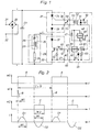
- a bridge rectifier is shown at 20, one diagonal of which is connected to two terminals 21 and 22 for connection to an AC distribution network.
- a DC voltage is created, which is smoothed by means of a capacitor 23.
- the bridge rectifier 20 and the capacitor 23 together form a direct current source for feeding a fluorescent lamp 24, the brightness of which should be adjustable.
- the fluorescent lamp 24 is assigned a ballast impedance 25, which has an electrical capacitor 26 and an induction coil 27.
- the fluorescent lamp 24 and the ballast impedance 25 together form a series circuit 28 which is connected on the one hand directly to the negative pole of the direct current source 20, 23 and on the other hand can be connected to the positive pole of the direct current source 20, 23 by means of a first electronic switch arrangement 31.
- a second electronic switch arrangement 32 lies parallel to the series connection 283.
- the first electronic switch arrangement 31 has a diode 33 and a controlled semiconductor rectifier 34, for example a thyristor, and two connecting terminals 35 and 36, which are connected to the cathode or the control electrode of the thyristor 34 and for supplying a clock signal u1 for controlling the Serve thyristors.
- the diode 33 and the thyristor 34 are arranged in series between the ' series circuit 28 and the positive pole of the direct current source 20, 23.
- the second electronic switch arrangement 32 has a diode 37, a power transistor 38, two electrical resistors 39 and 40 and two connecting terminals 41 and 42, which are used to supply a clock signal u2 to control the transistor 38.
- the diode 37 and the collector-emitter path of the transistor 38 are connected in series and arranged in parallel with the series circuit 28.
- One resistor 39 lies between the base and the emitter of transistor 38, while the other resistor 40 is connected between the base of the transistor on the one hand and terminal 42 on the other.
- the other terminal 41 is connected to the emitter of transistor 38.
- An electronic control device 45 is provided for generating the two clock signals ul and u2.
- This has one astable multivibrator 46, which is fed by an auxiliary power source 47 and generates an output signal u in the form of a sequence of rectangular voltage pulses A between a signal output 48 and a ground conductor 49, as shown in FIG. 2.
- the repetition frequency f 1 / T of the voltage pulses is adjustable.
- the signal output 48 of the multivibrator 46 is connected via a capacitor 50 to one end of the primary winding 51 of a pulse transformer 52, while the other end of the winding 51 is connected to the ground conductor 49.
- the secondary winding 53 of the pulse transformer which is electrically isolated from the primary winding 51, is connected to two output terminals 55 and 56, which are connected to the connecting terminals 35 and 36 of the first switch arrangement 31.
- Capacitor 50 transmits positive needle pulses on the rising edges of voltage pulses A of output signal u 0 and negative needle pulses on the falling edges.
- a diode 57 is connected in parallel to the primary winding 51 of the pulse transformer 52, so that the clock signal u.1 supplied to the connecting terminals 35 and 36 of the switch arrangement 31 only consists of positive needle pulses B, the duration W1 of which is relatively short, as in each case Fig. 2 shows.
- the signal output 48 of the astable multivibrator 46 is also connected via a second capacitor 60 to the signal input 61 of a monostable multivibrator 62, which is also fed from the auxiliary power source 47.
- a resistor 63 and a diode 64 lie between the input 61 and the ground conductor 49.
- Capacitor 60 transmits positive needle pulses on the rising edges of the voltage pulses A of the output signal u and negative needle pulses on the falling edges.
- the diode 64 suppresses the positive needle pulses, so that only negative needle pulses reach the signal input 61 of the astable multivibrator 62 on the falling edges of the output signal u o .
- a signal output 65 of the latter and the ground conductor 49 are each connected to a connecting terminal 66 or 67. These terminals 66 and 67 are connected to the connection terminals 41 and 42 of the second switch arrangement 32.
- the clock signal u2 supplied to the connecting terminals 41 and 42 of the second switch arrangement 32 thus consists of a sequence of rectangular pulses C, each of which has the duration W2, as can be seen in FIG. 2.
- the described processes are repeated in each subsequent period of the output signal u, so that positive current pulses D1 and negative current pulses D2 flow through the series circuit 28 and thus the fluorescent lamp 24, by means of which the lamp 24 is brought to light.
- the repetition frequency of the current pulse pairs D1, D2 corresponds to the repetition frequency f of the rectangular pulses A of the output signal u. If the frequency f is changed by a setting element (not shown) on the astable multivibrator 46, the time interval of the successive current pulses D1 and D2 also changes, while the shape and the duration of the individual current pulses D1 and D2 remain unchanged. If the frequency f is reduced, a smaller number of current pulses D1 and D2 occur per unit of time, the brightness of the fluorescent lamp 24 being reduced accordingly.
- the diodes 33 and 37 each serve to cause the current to swing back! at the end of preventing every current pulse D1 or D2.
- the auxiliary power source 47 does not need to be a battery, but can be replaced by a mains connection device or a circuit arrangement for deriving the auxiliary supply current from the direct current source 20, 23.
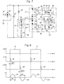
- the embodiment of the device for brightness regulation shown in simplified form in FIG. 3 differs from that according to FIG. 1 only in that in addition an electrical resistor 70 on the one hand to the positive pole of the direct current source 20, 23 and on the other hand at a point 71 between the capacitor 26 and the Induction coil 27 is connected.
- the resistance value of the resistor 70 is dimensioned such that a relatively weak direct current flows through the fluorescent lamp 24 and is superimposed on the current pulses D1 and D2 according to FIG. 2. This measure improves the ignition property of the fluorescent lamp 24.
- FIG. 4 illustrates in a simplified representation an embodiment of the device which differs from that according to FIG. 1 only in that the positions of the two electronic switch arrangements 31 and 32 are interchanged.
- the capacitor 26 is thus charged in each case the transistor 38 in control dependence on the rectangular voltage pulses C of the clock signal u2, and the capacitor 26 is discharged via the thyristor 34 in control dependence on the needle pulses B of the clock signal u1. Otherwise, the function and mode of operation of the device is the same as in the first exemplary embodiment according to FIGS. 1 and 2.
- the additional resistor 70 for improving the ignition property of the fluorescent lamp 24 can also be provided in the exemplary embodiment according to FIG. 4, as with dashed lines Lines is indicated.
- the electronic switch arrangement 31 containing the thyristor 34 can be replaced by a differently designed switch arrangement 131 according to FIG. 5.
- this now has a power transistor 75, which is no longer driven directly by the needle pulses B of the clock signal u1, but by a control signal u3 which is dependent on the clock signal u1 by means of a monostable multivibrator 76 is produced.
- the multivibrator 76 essentially consists of a two-stage DC voltage amplifier which has two transistors 77 and 78 and a number of resistors 79 to 84 and is fed back via a capacitor 85 and a resistor 86.
- the signal input 87 of the multivibrator 76 is connected to the connection terminal 36 via a capacitor 88, " while the signal output 89 of the multivibrator 76 is connected to the base of the power transistor 75.
- the ground conductor 90 of the multivibrator 76 is connected to both the connection terminal 35 and the Emitter of the power transistor 75.
- a storage capacitor 91 is provided as the energy source for supplying the monostable multivibrator 76, which on the one hand has the positive pole of the direct current source 20, 23 (FIG. 1) and on the other hand has a series resistor 92 with the negative pole of the direct current source 20, 23 is connected Limiting the DC voltage lying across the storage capacitor 91, a Zener diode 93 is connected in parallel with the storage capacitor 91.
- the power transistor 38 is in each case conductive for the duration W2 of a voltage pulse C, as a result of which the previously charged capacitor 26 is discharged and a current pulse D2 is generated, the polarity of which is opposite to that of the current pulses D1.
- the sequence of alternating current pulses D1 and D2 illuminates the fluorescent lamp 24, the brightness of the lamp depending on the repetition frequency of the pulses, as was explained in relation to the first exemplary embodiment.
- the arrangement of the storage capacitor 91 and the series resistor 92 shown in FIG. 5 makes a special auxiliary power source for the supply of the monostable multivibrator 76 unnecessary.
- the astable multivibrator 46 and the monostable multivibrator 62 can also be supplied in an analogous manner in the control device 45 (FIG. 1).
- FIG. 7 shows a device suitable for regulating the brightness of the fluorescent lamp 24, which essentially differs from that according to FIG. 1 in that instead of the electronic switch arrangement 32 (FIG. 1) having the power transistor 38, it is now the same as the first switch arrangement 31 trained second switch assembly 311 is present.
- the latter also has a thyristor 341, a diode 331 and two connecting terminals 351 and 361 for supplying a clock signal u11, which consists of a sequence of needle pulses B1, the duration W 11 of which approximately matches that of the needle pulses B of the clock signal u1.
- the control device for generating the two clock signals u1 and u11 has an astable multivibrator 46 and an auxiliary current source 47 serving to supply the same.
- the signal output 48 and the ground conductor 49 of the multivibrator 46 are connected via a capacitor 50 or directly to the ends of the primary winding 51 of a pulse transformer 52, the secondary winding 53 of which supplies the clock signal u1 to the output terminals 55 and 56.
- a diode 57 is the primary winding 51 of the pulse transformer connected in parallel in order to ensure that the clock signal u1 consists exclusively of needle pulses B which occur on the rising edges of the rectangular pulses A of the output signal u o .
- ground conductor 49 and the signal output 48 of the multivibrator 46 are connected directly or via a capacitor 94 to two output terminals 95 and 96, from which the clock signal u11 is passed to the connection terminals 351 and 361 of the circuit arrangement 311.
- a diode 97 and a resistor 98 are connected between the two output terminals 95 and 96 in order to ensure that the clock signal u11 consists exclusively of needle pulses B1, which occur in each case on the falling edges of the rectangular pulses A of the output signal u o .
- each of the thyristors 34 and 341 in the two electronic switch arrangements 31 and 311 is controlled by a needle pulse B and B1, the duration W1 and W11 of which is considerably shorter than the duration W i of the resulting current pulse D1 and D2.
- the thyristors remain in a conductive state by themselves as long as the current pulse in question lasts.
- the circuitry of the further exemplary embodiment illustrated in FIG. 9 differs from that according to FIG. 7 only in that instead of the two electronic switch arrangements 31 and 311 with one thyristor (FIG. 7), two mutually identical switch arrangements 131 with the configuration according to FIG. 5 are available.
- the two clock signals u1 and u11 which each consist of a sequence of needle pulses B and B1, respectively control the monostable multivibrator 76 (FIG. 5) in the relevant switch arrangement 131.
- These multivibrators each generate a control signal u3 or u31 in the form of a Sequence of rectangular voltage pulses E or E1 for controlling the associated power transistor 75 (FIG. 5).
- the latter is in the conductive state for the entire duration W3 or.W31 of the control pulse E or E1 in question.
- the resulting current pulses D1 and D2 in the series circuit 28 formed by the fluorescent lamp 24 and the ballast impedance 25 each have a duration W i which is slightly shorter than the duration W3 or W31 of the control pulses E and E1.
- FIG. 11 shows the circuit diagram of an embodiment of the brightness control device which differs from that according to FIG. 1 only in that instead of the pulse transformer 52 (FIG. 1) there is now an optoelectric signal transmission device 100.
- the latter has a light-emitting diode 101 serving as a light transmitter and a photo element 102 which acts as a light receiver and which supplies the clock signal u1 to the output terminals 55 and 56.
- the use and mode of operation of the device basically remains the same as has been described with reference to FIG. 2.
- the pulse transformer 52 can also be replaced by an optoelectric transmission device 100 according to FIG. 11.
- All of the described exemplary embodiments of the device according to the invention for regulating the brightness of a fluorescent lamp have in common that at least one of the two electronic switch arrangements 31, 32 or 131, 32 or 31, 311 or 131, 131 can be controlled by clock pulses, the duration of which W1 or W11 is short in comparison to the duration W i of each current pulse D1 or D2 through the lamp 24, and that the switch arrangement in question has a thyristor 34 or 341 or equivalent other circuit components 75 to 86, in each case by the conductive state of the circuit arrangement to maintain the duration of a single clock pulse throughout the duration of the current pulse in question.
- reliable operation of the control device is achieved without mutual interference between the two electronic switch arrangements.
- the ballast impedance 25 arranged in series with the fluorescent lamp 24 can, instead of the capacitor 26 and the induction coil 27, optionally also consist of a capacitor and a resistor or of a capacitor alone, in particular if the lamp 24 to be regulated in brightness has relatively low nominal power. Then, however, there is another, technically less favorable form of the current pulses D1 and D2.
- a second series circuit which consists of a fluorescent lamp and an associated ballast impedance, in parallel with the electronic switch arrangement 31 in FIGS. 1, 3, 7 and 11 or in series with the first series circuit 28. 32 in Fig. 4 and 131 in Fig. 9 (top) to be arranged.
- the capacitor 26 of the one ballast impedance 25 is charged while the capacitor of the second ballast impedance is being discharged, and vice versa. In this way, the brightness of two fluorescent lamps can be controlled in the same way in a relatively simple manner.
Landscapes
- Engineering & Computer Science (AREA)
- Power Engineering (AREA)
- Circuit Arrangements For Discharge Lamps (AREA)
- Inverter Devices (AREA)
- Discharge-Lamp Control Circuits And Pulse- Feed Circuits (AREA)
Applications Claiming Priority (2)
| Application Number | Priority Date | Filing Date | Title |
|---|---|---|---|
| CH1764/81 | 1981-03-16 | ||
| CH176481 | 1981-03-16 |
Publications (2)
| Publication Number | Publication Date |
|---|---|
| EP0060458A2 true EP0060458A2 (fr) | 1982-09-22 |
| EP0060458A3 EP0060458A3 (fr) | 1983-08-03 |
Family
ID=4218018
Family Applications (1)
| Application Number | Title | Priority Date | Filing Date |
|---|---|---|---|
| EP82101721A Withdrawn EP0060458A3 (fr) | 1981-03-16 | 1982-03-05 | Equipement pour régler la luminosité d'une lampe à fluorescence |
Country Status (5)
| Country | Link |
|---|---|
| EP (1) | EP0060458A3 (fr) |
| JP (1) | JPS58500632A (fr) |
| DK (1) | DK505782A (fr) |
| NO (1) | NO823820L (fr) |
| WO (1) | WO1982003307A1 (fr) |
Cited By (1)
| Publication number | Priority date | Publication date | Assignee | Title |
|---|---|---|---|---|
| EP0111296A1 (fr) * | 1982-12-10 | 1984-06-20 | Siemens Aktiengesellschaft | Dispositif pour contrôler l'intensité d'une lampe de décharge à basse pression |
Families Citing this family (1)
| Publication number | Priority date | Publication date | Assignee | Title |
|---|---|---|---|---|
| US7169874B2 (en) * | 2001-11-02 | 2007-01-30 | Bausch & Lomb Incorporated | High refractive index polymeric siloxysilane compositions |
Family Cites Families (3)
| Publication number | Priority date | Publication date | Assignee | Title |
|---|---|---|---|---|
| US3896336A (en) * | 1973-12-20 | 1975-07-22 | Texas Instruments Inc | Solid state fluorescent lamp ballast system |
| US4229681A (en) * | 1978-12-29 | 1980-10-21 | Gte Products Corporation | Frequency/sensitive switching circuit |
| JPS5856475B2 (ja) * | 1979-08-03 | 1983-12-15 | 株式会社東芝 | 誘導加熱調理器の発振回路 |
-
1982
- 1982-03-05 EP EP82101721A patent/EP0060458A3/fr not_active Withdrawn
- 1982-03-09 WO PCT/CH1982/000036 patent/WO1982003307A1/fr not_active Ceased
- 1982-03-09 JP JP57500837A patent/JPS58500632A/ja active Pending
- 1982-11-12 DK DK505782A patent/DK505782A/da not_active Application Discontinuation
- 1982-11-15 NO NO823820A patent/NO823820L/no unknown
Cited By (1)
| Publication number | Priority date | Publication date | Assignee | Title |
|---|---|---|---|---|
| EP0111296A1 (fr) * | 1982-12-10 | 1984-06-20 | Siemens Aktiengesellschaft | Dispositif pour contrôler l'intensité d'une lampe de décharge à basse pression |
Also Published As
| Publication number | Publication date |
|---|---|
| DK505782A (da) | 1982-11-12 |
| NO823820L (no) | 1982-11-15 |
| JPS58500632A (ja) | 1983-04-21 |
| EP0060458A3 (fr) | 1983-08-03 |
| WO1982003307A1 (fr) | 1982-09-30 |
Similar Documents
| Publication | Publication Date | Title |
|---|---|---|
| EP0338109B1 (fr) | Convertisseur pour lampe à décharge | |
| DE2903224C2 (de) | Schaltungsanordnung zum Zünden und Speisen einer mit einer vorheizbaren Elektrode versehenen Metalldampfentladungslampe | |
| DE2325872C2 (de) | Notstromversorgung für ein Beleuchtungssystem mit wenigstens zwei in Reihe geschalteten Entladungslampen | |
| DE2936088A1 (de) | Rechteck-dimmerschaltung mit feststehender frequenz und variablem impulsfaktor fuer hochleistungs-gasentladungslampen | |
| DE3886000T2 (de) | Elektrische Anordnung zum Zünden und Speisen einer Gasenladungslampe. | |
| DE3447486A1 (de) | Treiber zum betrieb eines elektrischen verbrauchers sowie mit einem solchen treiber aufgebautes steuergeraet oder steuereinrichtung | |
| DE2657450C2 (de) | Speiseschaltung für einen Mikrowellengenerator und Verfahren zum Betrieb eines Mikrowellengenerators eines Mikrowellen-Erhitzungsgerätes | |
| DE2827693A1 (de) | Wechselrichter und dessen verwendung in einem batterieladegeraet | |
| DE10201852A1 (de) | Entladungslampen-Beleuchtungseinrichtung | |
| DE3403619A1 (de) | Elektrische stromversorgungsquelle fuer die verwendung in einer elektrostatischen ausfaellvorrichtung | |
| DE2824326A1 (de) | Stromversorgung fuer elektrische bearbeitung | |
| DE19729768B4 (de) | Schaltungsanordnung zum Zünden und Betreiben einer Leuchtstofflampe | |
| DE3248388C2 (de) | Elektronische Zündschaltung für eine Brennkraftmaschine | |
| DE69017940T2 (de) | Wechselrichter zum Speisen zweier Gas und / oder Dampfentladungslampen. | |
| DE69512606T2 (de) | Leistungsversorgungseinrichtung mit leistungsfaktorverbesserungsschaltung | |
| DE3400580C2 (fr) | ||
| DE2360263B2 (de) | Schaltungsanordnung zum Zünden einer Gas- und/oder Dampfentladungslampe | |
| DE3610156C2 (fr) | ||
| DE4133027C2 (de) | Zündvorrichtung für eine Verbrennungskraftmaschine | |
| DE3338464A1 (de) | Hochfrequenz-helligkeitssteuerung fuer leuchtstofflampen | |
| DE3005160A1 (de) | Ansteuerschaltung fuer eine blitzlampe | |
| EP0060458A2 (fr) | Equipement pour régler la luminosité d'une lampe à fluorescence | |
| DE3343930A1 (de) | Schaltungsanordnung zum betrieb von leuchtstoff- oder ultraviolett-niederspannungs-entladungslampen | |
| EP0722263B1 (fr) | Circuit pour le préchauffage des électrodes d'une lampe fluorescente | |
| DE2746099A1 (de) | Wechselrichter mit mindestens zwei steuerbaren lastthyristoren |
Legal Events
| Date | Code | Title | Description |
|---|---|---|---|
| PUAI | Public reference made under article 153(3) epc to a published international application that has entered the european phase |
Free format text: ORIGINAL CODE: 0009012 |
|
| AK | Designated contracting states |
Kind code of ref document: A2 Designated state(s): AT BE DE FR GB IT NL SE |
|
| PUAL | Search report despatched |
Free format text: ORIGINAL CODE: 0009013 |
|
| AK | Designated contracting states |
Kind code of ref document: A3 Designated state(s): AT BE DE FR GB IT NL SE |
|
| STAA | Information on the status of an ep patent application or granted ep patent |
Free format text: STATUS: THE APPLICATION HAS BEEN WITHDRAWN |
|
| 18W | Application withdrawn |
Withdrawal date: 19840203 |
|
| RIN1 | Information on inventor provided before grant (corrected) |
Inventor name: JUCKER, PETER |