EP0061923A1 - Halbleiteranordnung mit einer dünnen polykristallinen Schicht - Google Patents
Halbleiteranordnung mit einer dünnen polykristallinen Schicht Download PDFInfo
- Publication number
- EP0061923A1 EP0061923A1 EP82301643A EP82301643A EP0061923A1 EP 0061923 A1 EP0061923 A1 EP 0061923A1 EP 82301643 A EP82301643 A EP 82301643A EP 82301643 A EP82301643 A EP 82301643A EP 0061923 A1 EP0061923 A1 EP 0061923A1
- Authority
- EP
- European Patent Office
- Prior art keywords
- polycrystalline
- semiconductor film
- film
- thin film
- polycrystalline semiconductor
- Prior art date
- Legal status (The legal status is an assumption and is not a legal conclusion. Google has not performed a legal analysis and makes no representation as to the accuracy of the status listed.)
- Granted
Links
Images


Classifications
-
- H—ELECTRICITY
- H10—SEMICONDUCTOR DEVICES; ELECTRIC SOLID-STATE DEVICES NOT OTHERWISE PROVIDED FOR
- H10P—GENERIC PROCESSES OR APPARATUS FOR THE MANUFACTURE OR TREATMENT OF DEVICES COVERED BY CLASS H10
- H10P14/00—Formation of materials, e.g. in the shape of layers or pillars
- H10P14/20—Formation of materials, e.g. in the shape of layers or pillars of semiconductor materials
- H10P14/29—Formation of materials, e.g. in the shape of layers or pillars of semiconductor materials characterised by the substrates
- H10P14/2901—Materials
- H10P14/2921—Materials being crystalline insulating materials
-
- H—ELECTRICITY
- H10—SEMICONDUCTOR DEVICES; ELECTRIC SOLID-STATE DEVICES NOT OTHERWISE PROVIDED FOR
- H10D—INORGANIC ELECTRIC SEMICONDUCTOR DEVICES
- H10D30/00—Field-effect transistors [FET]
- H10D30/60—Insulated-gate field-effect transistors [IGFET]
- H10D30/67—Thin-film transistors [TFT]
- H10D30/674—Thin-film transistors [TFT] characterised by the active materials
- H10D30/6741—Group IV materials, e.g. germanium or silicon carbide
-
- H—ELECTRICITY
- H10—SEMICONDUCTOR DEVICES; ELECTRIC SOLID-STATE DEVICES NOT OTHERWISE PROVIDED FOR
- H10D—INORGANIC ELECTRIC SEMICONDUCTOR DEVICES
- H10D30/00—Field-effect transistors [FET]
- H10D30/60—Insulated-gate field-effect transistors [IGFET]
- H10D30/67—Thin-film transistors [TFT]
- H10D30/674—Thin-film transistors [TFT] characterised by the active materials
- H10D30/6741—Group IV materials, e.g. germanium or silicon carbide
- H10D30/6743—Silicon
- H10D30/6745—Polycrystalline or microcrystalline silicon
-
- H—ELECTRICITY
- H10—SEMICONDUCTOR DEVICES; ELECTRIC SOLID-STATE DEVICES NOT OTHERWISE PROVIDED FOR
- H10D—INORGANIC ELECTRIC SEMICONDUCTOR DEVICES
- H10D62/00—Semiconductor bodies, or regions thereof, of devices having potential barriers
- H10D62/40—Crystalline structures
-
- H—ELECTRICITY
- H10—SEMICONDUCTOR DEVICES; ELECTRIC SOLID-STATE DEVICES NOT OTHERWISE PROVIDED FOR
- H10D—INORGANIC ELECTRIC SEMICONDUCTOR DEVICES
- H10D62/00—Semiconductor bodies, or regions thereof, of devices having potential barriers
- H10D62/80—Semiconductor bodies, or regions thereof, of devices having potential barriers characterised by the materials
- H10D62/83—Semiconductor bodies, or regions thereof, of devices having potential barriers characterised by the materials being Group IV materials, e.g. B-doped Si or undoped Ge
- H10D62/834—Semiconductor bodies, or regions thereof, of devices having potential barriers characterised by the materials being Group IV materials, e.g. B-doped Si or undoped Ge further characterised by the dopants
-
- H—ELECTRICITY
- H10—SEMICONDUCTOR DEVICES; ELECTRIC SOLID-STATE DEVICES NOT OTHERWISE PROVIDED FOR
- H10D—INORGANIC ELECTRIC SEMICONDUCTOR DEVICES
- H10D8/00—Diodes
-
- H—ELECTRICITY
- H10—SEMICONDUCTOR DEVICES; ELECTRIC SOLID-STATE DEVICES NOT OTHERWISE PROVIDED FOR
- H10F—INORGANIC SEMICONDUCTOR DEVICES SENSITIVE TO INFRARED RADIATION, LIGHT, ELECTROMAGNETIC RADIATION OF SHORTER WAVELENGTH OR CORPUSCULAR RADIATION
- H10F77/00—Constructional details of devices covered by this subclass
- H10F77/10—Semiconductor bodies
- H10F77/16—Material structures, e.g. crystalline structures, film structures or crystal plane orientations
- H10F77/162—Non-monocrystalline materials, e.g. semiconductor particles embedded in insulating materials
- H10F77/164—Polycrystalline semiconductors
- H10F77/1642—Polycrystalline semiconductors including only Group IV materials
-
- H—ELECTRICITY
- H10—SEMICONDUCTOR DEVICES; ELECTRIC SOLID-STATE DEVICES NOT OTHERWISE PROVIDED FOR
- H10P—GENERIC PROCESSES OR APPARATUS FOR THE MANUFACTURE OR TREATMENT OF DEVICES COVERED BY CLASS H10
- H10P14/00—Formation of materials, e.g. in the shape of layers or pillars
- H10P14/20—Formation of materials, e.g. in the shape of layers or pillars of semiconductor materials
- H10P14/22—Formation of materials, e.g. in the shape of layers or pillars of semiconductor materials using physical deposition, e.g. vacuum deposition or sputtering
-
- H—ELECTRICITY
- H10—SEMICONDUCTOR DEVICES; ELECTRIC SOLID-STATE DEVICES NOT OTHERWISE PROVIDED FOR
- H10P—GENERIC PROCESSES OR APPARATUS FOR THE MANUFACTURE OR TREATMENT OF DEVICES COVERED BY CLASS H10
- H10P14/00—Formation of materials, e.g. in the shape of layers or pillars
- H10P14/20—Formation of materials, e.g. in the shape of layers or pillars of semiconductor materials
- H10P14/24—Formation of materials, e.g. in the shape of layers or pillars of semiconductor materials using chemical vapour deposition [CVD]
-
- H—ELECTRICITY
- H10—SEMICONDUCTOR DEVICES; ELECTRIC SOLID-STATE DEVICES NOT OTHERWISE PROVIDED FOR
- H10P—GENERIC PROCESSES OR APPARATUS FOR THE MANUFACTURE OR TREATMENT OF DEVICES COVERED BY CLASS H10
- H10P14/00—Formation of materials, e.g. in the shape of layers or pillars
- H10P14/20—Formation of materials, e.g. in the shape of layers or pillars of semiconductor materials
- H10P14/29—Formation of materials, e.g. in the shape of layers or pillars of semiconductor materials characterised by the substrates
- H10P14/2901—Materials
- H10P14/2923—Materials being conductive materials, e.g. metallic silicides
-
- H—ELECTRICITY
- H10—SEMICONDUCTOR DEVICES; ELECTRIC SOLID-STATE DEVICES NOT OTHERWISE PROVIDED FOR
- H10P—GENERIC PROCESSES OR APPARATUS FOR THE MANUFACTURE OR TREATMENT OF DEVICES COVERED BY CLASS H10
- H10P14/00—Formation of materials, e.g. in the shape of layers or pillars
- H10P14/20—Formation of materials, e.g. in the shape of layers or pillars of semiconductor materials
- H10P14/32—Formation of materials, e.g. in the shape of layers or pillars of semiconductor materials characterised by intermediate layers between substrates and deposited layers
- H10P14/3202—Materials thereof
- H10P14/3204—Materials thereof being Group IVA semiconducting materials
- H10P14/3211—Silicon, silicon germanium or germanium
-
- H—ELECTRICITY
- H10—SEMICONDUCTOR DEVICES; ELECTRIC SOLID-STATE DEVICES NOT OTHERWISE PROVIDED FOR
- H10P—GENERIC PROCESSES OR APPARATUS FOR THE MANUFACTURE OR TREATMENT OF DEVICES COVERED BY CLASS H10
- H10P14/00—Formation of materials, e.g. in the shape of layers or pillars
- H10P14/20—Formation of materials, e.g. in the shape of layers or pillars of semiconductor materials
- H10P14/34—Deposited materials, e.g. layers
- H10P14/3402—Deposited materials, e.g. layers characterised by the chemical composition
- H10P14/3404—Deposited materials, e.g. layers characterised by the chemical composition being Group IVA materials
- H10P14/3411—Silicon, silicon germanium or germanium
-
- H—ELECTRICITY
- H10—SEMICONDUCTOR DEVICES; ELECTRIC SOLID-STATE DEVICES NOT OTHERWISE PROVIDED FOR
- H10P—GENERIC PROCESSES OR APPARATUS FOR THE MANUFACTURE OR TREATMENT OF DEVICES COVERED BY CLASS H10
- H10P14/00—Formation of materials, e.g. in the shape of layers or pillars
- H10P14/20—Formation of materials, e.g. in the shape of layers or pillars of semiconductor materials
- H10P14/34—Deposited materials, e.g. layers
- H10P14/3438—Doping during depositing
- H10P14/3441—Conductivity type
- H10P14/3442—N-type
-
- H—ELECTRICITY
- H10—SEMICONDUCTOR DEVICES; ELECTRIC SOLID-STATE DEVICES NOT OTHERWISE PROVIDED FOR
- H10P—GENERIC PROCESSES OR APPARATUS FOR THE MANUFACTURE OR TREATMENT OF DEVICES COVERED BY CLASS H10
- H10P14/00—Formation of materials, e.g. in the shape of layers or pillars
- H10P14/20—Formation of materials, e.g. in the shape of layers or pillars of semiconductor materials
- H10P14/34—Deposited materials, e.g. layers
- H10P14/3438—Doping during depositing
- H10P14/3441—Conductivity type
- H10P14/3444—P-type
-
- Y—GENERAL TAGGING OF NEW TECHNOLOGICAL DEVELOPMENTS; GENERAL TAGGING OF CROSS-SECTIONAL TECHNOLOGIES SPANNING OVER SEVERAL SECTIONS OF THE IPC; TECHNICAL SUBJECTS COVERED BY FORMER USPC CROSS-REFERENCE ART COLLECTIONS [XRACs] AND DIGESTS
- Y02—TECHNOLOGIES OR APPLICATIONS FOR MITIGATION OR ADAPTATION AGAINST CLIMATE CHANGE
- Y02E—REDUCTION OF GREENHOUSE GAS [GHG] EMISSIONS, RELATED TO ENERGY GENERATION, TRANSMISSION OR DISTRIBUTION
- Y02E10/00—Energy generation through renewable energy sources
- Y02E10/50—Photovoltaic [PV] energy
- Y02E10/546—Polycrystalline silicon PV cells
-
- Y—GENERAL TAGGING OF NEW TECHNOLOGICAL DEVELOPMENTS; GENERAL TAGGING OF CROSS-SECTIONAL TECHNOLOGIES SPANNING OVER SEVERAL SECTIONS OF THE IPC; TECHNICAL SUBJECTS COVERED BY FORMER USPC CROSS-REFERENCE ART COLLECTIONS [XRACs] AND DIGESTS
- Y10—TECHNICAL SUBJECTS COVERED BY FORMER USPC
- Y10S—TECHNICAL SUBJECTS COVERED BY FORMER USPC CROSS-REFERENCE ART COLLECTIONS [XRACs] AND DIGESTS
- Y10S438/00—Semiconductor device manufacturing: process
- Y10S438/958—Passivation layer
Definitions
- the present invention relates to a polycrystalline thin film, and more particularly to a semiconductor device having a silicon polycrystalline semiconductor thin film.
- the polycrystalline thin film has properties that it is easier to fabricate than a monocrystalline thin film and has a better electrical characteristic such as larger mobility of carriers than an amorphous thin film.
- the polycrystalline thin film has not been widely used as a body of an electronic active device because. of degradation of the electrical characteristics due to various defects present at crystal grain boundaries.
- the characteristic of the active device is degraded because dangling bonds of constituent atoms which are mainly present at polycrystal grain boundaries are electrically active and act as recombination centers or carrier scattering centers or cause grain boundary diffusion of impurities.
- the semi- conductor thin film having many crystal grain boundaries is not proper to use in a semiconductor device having a pn junction.
- a typical example of the semiconductor device having the polycrystal is disclosed in "Deposition and Properties of Polycrystalline Silicon Films for Solar Cells" Digest of Technical Papers. The lst PHOTOVOLTAIC SCIENCE and ENGINEERING CONFERENCE IN JAPAN, Nov. 6-8, 1979 (Tokyo) pages 1-2.
- a polycrystalline semiconductor thin film having at least one element selected from a group consisting of hydrogen, fluorine, chlorine, bromine, iodine, lithium, sodium, potassium, rubidium and cesium included mainly around the grain boundaries of the polycrystalline semi- conductor thin film is used as the body of the semi- conductor device.
- the content of the element or elements varies depending on crystal grain size and a total content of 100 ppm by atomic ratio to 40 atom % in average of the film is preferable.
- the dangling bonds which are present mainly around the grain boundaries of the polycrystalline semiconductor thin film form electrically active localized levels in a forbidden band of the semiconductors, and a density of the localized levels can be decreased by adding appropriate monovalent atoms to the dangling bonds.
- the density of the localized level can be reduced by adding the above- mentioned monovalent element such as hydrogen or fluoride to the body of the polycrystalline semiconductor which includes many dangling bonds.
- the above effect is not only observed in the polycrystalline silicon film but also more or less observed in a mixed crystal such as polycrystalline silicon-germanium, a III-V group compound such as polycrystalline gallium arsenide or a II-VI group compound such as polycrystalline cadmium sulfide.
- a mixed crystal such as polycrystalline silicon-germanium, a III-V group compound such as polycrystalline gallium arsenide or a II-VI group compound such as polycrystalline cadmium sulfide.
- silicon content is more than 50% of a total content
- various localized levels are apt to be formed because chemical activity of the dangling bonds at the grain boundaries is high. Accordingly, the present method for reducing the localized levels by the adding of the monovalent element is particularly effective to such monocrystal.
- a grain size of the monocrystal to which the present invention is applicable may range from several nanometers at minimum to several millimeters at maximum. In general, it may be considered as non-single crystal other than that from which a perfect halo pattern is observed by an electron beam diffraction or an X-ray diffraction, that is, the non-single crystal from which a ring pattern or a spot pattern indicating an orientation. In such a polycrystal, it is considered that atoms are relatively regularly arranged in the respective crystal grains and the dangling bonds concentrate around the grain boundaries. Accordingly, the monovalent element for reducing the localized level must be added around the monocrystalline grain boundaries.
- the content of the monovalent element included in the polycrystal may be 100 ppm by atomic ratio in average of the film in order to offer the effect of the present invention, but when the grain size of the crystal is small to approach amorphous state, the content may reach as much as 40 atom %. In the latter case, it may be considered to be nearly mixed state of amorphous material and fine crystal grains although a main body is a polycrystal. In this case, the densities of the localized levels at the boundaries of the amorphous material and the crystal grains can be reduced so that electronic material useful as photoconductor or fluorescent material can be provided.
- a metal plate such as iron, stainless steel, nickel or aluminum, a ceramics such as alumina, a glass plate such as quartz or hard glass, or organic material such as polyimide may be used.
- One of the objects of the present invention is to impart to substrate material used to form a single crystal or a polycrystalline semiconductor thin film formed without satisfying a substrate temperature condition, a characteristic analogous to a single crystal usable as electronic material (such as mobility or photoconductivity).
- a substrate which is heterogeneous to a semiconductor substrate may be used. In order to minimize contamination by impurity diffusion from the substrate in such a case, it is desirable to keep a forming temperature of the polycrystalline semiconductor thin film at a low level. While a maximum temperature is restricted depending on a type of the substrate, an upper limit is approximately 700°C at which reaction between a metallic substrate and the semiconductor and a metal diffusion into the polycrystalline semiconductor thin film are hard to occur.
- the heat treatment in the plasma environment is carried out in the following condition; an environment gas pressure is 10 -3 pa - 10 pa, a substrate temperature is 350°C - 650°C, an RF input power is 0.03 W/ cm 2 - 10 W/cm and an RF frequency is 13.56 MHz although it is not limited thereto.
- the selected element may be introduced during the formation of the polycrystalline semiconductor thin film.
- the polycrystalline semiconductor thin film may be formed by silicon sputtering in a SiF 4 or SiCl 4 environement which is a silicon halide, glow-discharge decomposition of SiF 4 , forming GaAs polycrystal by reacting Ga with AsCl 3 by glow discharging, or forming a CdS polycrystalline thin film by associating cadmium ions, sulfur ions and hydrogen ions and ion-plating it to a substrate.
- the thickness of the polycrystalline semi- conductor thin film thus formed is preferably 100 nanometers at minimum because too thin film may affect -to the characteristic due to disturbance of crystal structure around an interface to the substrate.
- the thickness of the polycrystalline semiconductor thin film of 100 ⁇ m at maximum is sufficient.
- the polycrystalline semi- conductor thin film is too thick, it is difficult to externally add monovalent metal to the polycrystal.
- the polycrystalline semiconductor thin film of the present invention is formed at a low temperature and the density of the localized level due to the dangling bonds around the crystal grain boundaries is reduced by adding the monovalent element. Accordingly, a pn junction and a Schottky contact having a good characteristic, which could not be attained by the prior art polycrystalline thin film, can be formed.
- the pn junction is formed by superimposing a film doped with p-type impurity and a film doped with n-type impurity in the direction of the thickness of the films.
- a pnp or npn transistor is formed by superimposing a further layer thereon.
- the thin film pn junction and the Schottky contact can be used as a photo-sensing device with a large area, and a junction type or MOS type field effect transistor can be formed by utilizing a depletion layer of the junction or an insulating thin film formed on the polycrystalline thin film.
- a junction type or MOS type field effect transistor can be formed by utilizing a depletion layer of the junction or an insulating thin film formed on the polycrystalline thin film.
- halogen X is at least one element selected from F, Cl, Br and I
- M + is at least one of hydrogen H and monovalent metals Li, Na, K and Cs
- the halogen element such as fluorine which quenches the dangling bonds and is charged negatively and the cations such as lithium ions which quench the dangling bonds and are charged positively are sequentially added to neutralize the charges. Since the halogen element which is negatively charged has a large ion radius, it is preferable to introduce it during the formation of the polycrystalline thin film rather than after the formation thereof. On the other hand, the cation which is positively charged has a small ion radius and hence it can be readily introduced after the formation of the polycrystalline thin film.
- fluorine and hydrogen are simultaneously introduced in the following manner.
- a polycrystalline thin film having fluorine elements introduced mainly at the grain boundaries is formed on a substrate by silicon sputtering in a mixed environment of argon and SiF 4 .
- a sputter taget is a highly pure silicon crystal
- a partial pressure of SiF 4 is 10 pa - 10 pa (a total gas pressure is also 10 -3 pa - 10 pa)
- a substrate temperature is 550°C - 650°C
- a sputter RF input power is 0.5 W/cm - 10 W/cm 2
- an RF frequency is usually 13.56 MHz.
- Heat treatment is carried out at a plasma center containing cations.
- the treatment condition was set forth above.
- the present method of introducing the impurity can eliminate the following shortcoming.
- the crystal grain boundaries are quenched by fluorine, the dangling bonds at the grain boundaries are quenched, but because of a large electrical negative property of the fluorine atom F, the grain boundaries are charged negatively.
- a large electrical negative property of the fluorine atom F the grain boundaries are charged negatively.
- a large leak current is produced.
- TFT n-channel thin film transistor
- an n-channel is broken by a p-type region of the grain boundaries and a mobility is extremely reduced.
- the above method for introducing the impurity can resolve such a difficulty. The effect is more remarkable when the contents of the halogen element and the element selected from the group consisting of hydrogen and monovalent metal elements are 100 ppm to 10% by atom ratio, respectively.
- Table 2 shows densities of the localized levels of those samples measured by a field effect method before and after the heat treatment.
- the reduction of the density of the localized level of the sample heat- treated in the monovalent element glow discharge is remarkable. It is, therefore, considered that the increase of the photoconductivity of the samples is due to the reduction of the density of the localized levels which act as the recombination centers.
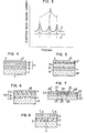
- Fig. 3 shows electron beam induced currents measured for the polycrystalline silicon films with and without hydrogen plasma treatment.
- a curve a shows the former case and a curve b shows the latter case.
- a chain line c shows a position corresponding to a crystal grain boundary.
- a polycrystalline silicon of 1 ⁇ m thick was formed on a quartz substrate at a substrate temperature of 600°C under an ultra-high vacuum of 2 x 10 -7 P a by a molecular beam deposition method.
- the resulting polycrystalline silicon was treated by an RF input power of 50 W at 13.56 MHz in a hydrogen environment of 0.05 Torr.
- the substrate temperature during the plasma treatment was 400°C and the treatment time was 30 minutes.
- the electron mobility of the sample was 20 cm 2 /V ⁇ sec while that of the untreated sample was 3 cm 2 /V.sec. Thus, a remarkable effect was observed.
- the present invention reduces the density of the localized level and improves the photoconductivity characteristic and the carrier mobility.
- Fig. 4 shows a sectional view of a solar cell.
- a stainless steel substrate 7 is placed in a vacuum chamber, and a polycrystalline silicon film 11 is deposited thereon by a glow discharge method at a substrate temperature of 600°C in an environment of gas mixture of SiF 4 and monosilane under a pressure of 2.7 pa.
- the forming condition is shown in Table 3.
- phosphine (PH 3 ) gas is introduced as an impurity source at a pressure of 1.3 x 10 -3 pa, and at an end stage diborane (B 2 H 6 ) gas is introduced at a pressure of 1.3 x 10 pa to form an n-i-p structure.
- the thickness of an n-layer 8, an i-layer 9 and a p-layer 10 are 300 nm, 5 ⁇ m and 100 nm, respectively. Thereafter, an indicum tin oxide film 12 of 300 nm thick is formed on the p-type polycrystalline silicon film by an RF sputtering device to form a transparent electrode.
- the resulting film can be used as a thin film solar cell having two electrodes of the stainless steel substrate and the transparent electrode. It has a photoelectric conversion efficiency of 8%. In the present example, it is essential that fluorine and hydrogen are included in the silicon film.
- the impurity densities in the n-layer, the i-layer and the p-layer are shown in Table 4.
- Fig. 5 shows a sectional view of a semiconductor device having a fluorescent film as an electroluminescence plate.
- a transparent electrode 14 is formed on a glass substrate 14 by a conventional method and then a blocking layer 15 is formed by Si 3 N 4 having a thick- 0 ness of 1000 A.
- the glass substrate 13 is then placed in a vacuum chamber and a ZnS: Mn fluorescent material 16 is vapor deposited thereon to the thickness of 0 approximately 3000 A at a substrate temperature of 300°C under vacuum of 7 x 10 -5 Torr.
- the fluorescent film is placed in a Na plasma formed in an environment of approximately 6 pa and heat treated at 500°C for one hour.
- a blocking layer 17 is formed by Si 3 N 4 0 having a thickness of 1000 A and a transparent electrode 18 is formed thereon.
- the electroluminescent plate thus formed has a higher photoelectric conversion efficiency than a fluorescent plate formed by other method and it can be used as a fluorescent plate such as electroluminescent plate.
- Polycrystalline silicon is deposited on a quartz or hard glass substrate kept at 500°C by molecular beam sources of silicon (Si), fluorine (F) and hydrogen (H).
- the molecular beam sources are such that fluorine is 0.5 atomic % to silicon and hydrogen is 1.0 atom % to silicon.
- fluorine (F) and hydrogen (H) are introduced so that they combine with silicon (Si) mainly at the polycrystal grain boundaries to quench the dangling bonds.
- Extra fluorine (F) and hydrogen (H) are evacuated from a molecular beam epitaxy equipment through an exhaust port.
- a boron (B) or antimony (Sb) molecular beam source is used in the formation of the film to add B or Sb as an impurity.
- FIG. 6 shows a sectional view of a diode.
- ITO indium tin oxide
- a polycrystalline silicon film 19 is formed on the substrate at a substrate temperature of 500°C by the molecular beam sources of silicon, fluorine and hydrogen conditioned as set forth above.
- Boron (B) is simultaneously deposited during the formation of a film 16 to make it p-type. Boron content is 0.05 atom % to silicon.
- the thickness of the film 16 is 0.2 ⁇ m.
- Antimony (Sb) is simultaneously deposited during the formation of a polycrystal silicon film 17 to make it n-type. Antimony content is 0.05 atom % to silicon.
- the thickness of the film 17 is 1.0 ⁇ m.
- a second electrode 18 is formed thereon to complete the semiconductor device. A substantial reduction of a leak current was observed.
- a polycrystalline silicon film 21 is deposited on a fuzed quartz or hard glass substrate 20 kept at 550°C, from a polycrystalline silicon target in a sputtering environment of gas mixture of SiF 4 and argon (Ar). Conditions for the preparation of samples are shown in Table 5. Thereafter, the sputtering equipment is evacuated to 10 pa and then H 2 gas is introduced to approximately 1 pa and an RF power of 13.56 MHz is applied to cause glow discharge (0.2 W/cm 2 ). The polycrystalline silicon film is kept at 350°C and left in the glow discharge for 30 minutes. As a result, a polycrystalline silicon film having grain boundaries thereof quenched by fluorine (F) and hydrogen (H) is produced.
- a Si0 2 film 22 having a thickness of 0 5000 A is deposited at a substrate temperature of 415°C by a vapor growth method.
- Windows for a source region 23 and a drain region 24 are formed in the SiO 2 film 22.
- BF 2 + ions of an energy of 150 KeV are implanted at a dose rate of 3 x 10 15 /cm 2 and the film is heat treated at 550°C for 100 minutes to form the P + layers 23 and 24 in the drain and source regions.
- the SiO 2 film is removed while leaving a field oxidiza-0 tion film.
- a SiO 2 film 28 (28') of 2000 A thick for a gate oxidization film is deposited by the vapor growth method.
- Electrode contact openings are formed by photolithographic method, an Al film is deposited on the entire surface and the Al film is lapped to form a source electrode 25, a drain electrode 27 and a gate electrode 26.
- the substrate is then heat treated at 400°C for 30 minutes in an H 2 environment to complete the semiconductor device.
- the polycrystalline silicon film of the present example was heated and a temperature at which hydrogen (H) was reemitted was measured. It was 700°C. This is much higher than the temperature of 350°C at which hydrogen is emitted when the film was passivated only by hydrogen.
- n-type and p-type carrier mobilities of the polycrystalline silicon film reaches as high as 20 cm 2 /v.sec. It indicates that the scatter at the grain boundaries is remarkably reduced.
- a conventional polycrystal has a carrier mobility of 1 - 10 cm 2 /V.sec. Accordingly, the integration of C-MOS thin film transistors is facilitated.
- Fig. 8 shows a sectional view of a transistor.
- a chromium film of 100 mm thick is vacuum deposited on a quartz substrate 1, and a gate electrode 2 is formed by photoetching process.
- An Si0 2 film 3 of 100 mm thick is deposited thereon by a CVD (chemical vapor deposition) process and the substrate is mounted on a vacuum deposition device.
- a polycrystalline silicon film 4 of 1 ⁇ m thick is formed at a substrate temperature of 450°C under vacuum of 3 x 10 -7 pa by an electron beam deposition method. The formation rate of the polycrystalline silicon film is 0.3 nm/sec. Then the substrate temperature is lowered to 250°C and the substrate is heat treated for 60 minutes in a glow discharge while introducing hydrogen gas at 4 pa.
- the hydrogen content is approximately 0.8 at %.
- B-impurity regions are formed at the regions (5, 6) corresponding to source and drain regions by a conventional ion implantation technique. Then, an aluminum film of 100 nm thick is vacuum deposited at a substrate temperature of 200°C under vacuum of 3 x 10 -7 pa. The sample is taken out of the vacuum deposition device and the source and drain, electrodes are formed by a photolithography technique to complete a field effect transistor.
Landscapes
- Thin Film Transistor (AREA)
- Photovoltaic Devices (AREA)
- Physical Deposition Of Substances That Are Components Of Semiconductor Devices (AREA)
- Recrystallisation Techniques (AREA)
Applications Claiming Priority (2)
| Application Number | Priority Date | Filing Date | Title |
|---|---|---|---|
| JP56045553A JPS57160123A (en) | 1981-03-30 | 1981-03-30 | Semiconductor device |
| JP45553/81 | 1981-03-30 |
Publications (2)
| Publication Number | Publication Date |
|---|---|
| EP0061923A1 true EP0061923A1 (de) | 1982-10-06 |
| EP0061923B1 EP0061923B1 (de) | 1988-05-18 |
Family
ID=12722546
Family Applications (1)
| Application Number | Title | Priority Date | Filing Date |
|---|---|---|---|
| EP82301643A Expired EP0061923B1 (de) | 1981-03-30 | 1982-03-29 | Halbleiteranordnung mit einer dünnen polykristallinen Schicht |
Country Status (6)
| Country | Link |
|---|---|
| US (1) | US4613382A (de) |
| EP (1) | EP0061923B1 (de) |
| JP (1) | JPS57160123A (de) |
| KR (1) | KR860001161B1 (de) |
| CA (1) | CA1189940A (de) |
| DE (1) | DE3278527D1 (de) |
Cited By (4)
| Publication number | Priority date | Publication date | Assignee | Title |
|---|---|---|---|---|
| DE3241959A1 (de) * | 1981-11-13 | 1983-05-26 | Canon K.K., Tokyo | Halbleiterbauelement |
| EP0129037A1 (de) * | 1983-06-17 | 1984-12-27 | Texas Instruments Incorporated | Polysilicium-FETs |
| EP0417942A1 (de) * | 1989-08-31 | 1991-03-20 | Tonen Corporation | Herstellung von aus polykristallinem Silizium bestehenden Dünnschichten und damit hergestellte Transistoren |
| US5111260A (en) * | 1983-06-17 | 1992-05-05 | Texax Instruments Incorporated | Polysilicon FETs |
Families Citing this family (24)
| Publication number | Priority date | Publication date | Assignee | Title |
|---|---|---|---|---|
| DE3300400A1 (de) * | 1982-01-06 | 1983-07-14 | Canon K.K., Tokyo | Halbleiterbauelement |
| US4670763A (en) * | 1984-05-14 | 1987-06-02 | Energy Conversion Devices, Inc. | Thin film field effect transistor |
| US4727044A (en) * | 1984-05-18 | 1988-02-23 | Semiconductor Energy Laboratory Co., Ltd. | Method of making a thin film transistor with laser recrystallized source and drain |
| US4717681A (en) * | 1986-05-19 | 1988-01-05 | Texas Instruments Incorporated | Method of making a heterojunction bipolar transistor with SIPOS |
| US4821091A (en) * | 1986-07-22 | 1989-04-11 | The United States Of America As Represented By The United States Department Of Energy | Polysilicon photoconductor for integrated circuits |
| US4945065A (en) * | 1988-06-02 | 1990-07-31 | Mobil Solar Energy Corporation | Method of passivating crystalline substrates |
| JPH0323639A (ja) * | 1989-06-21 | 1991-01-31 | Sony Corp | 薄膜トランジスタ |
| US5051786A (en) * | 1989-10-24 | 1991-09-24 | Mcnc | Passivated polycrystalline semiconductors quantum well/superlattice structures fabricated thereof |
| JPH0828379B2 (ja) * | 1990-05-28 | 1996-03-21 | 株式会社東芝 | 半導体装置の製造方法 |
| DE69125886T2 (de) * | 1990-05-29 | 1997-11-20 | Semiconductor Energy Lab | Dünnfilmtransistoren |
| JPH0611705A (ja) * | 1992-01-31 | 1994-01-21 | Sony Corp | 能動素子基板 |
| JPH06151801A (ja) * | 1992-11-13 | 1994-05-31 | Canon Inc | 光電変換装置及び光電変換装置の製造方法 |
| US5620906A (en) | 1994-02-28 | 1997-04-15 | Semiconductor Energy Laboratory Co., Ltd. | Method for producing semiconductor device by introducing hydrogen ions |
| US5897346A (en) * | 1994-02-28 | 1999-04-27 | Semiconductor Energy Laboratory Co., Ltd. | Method for producing a thin film transistor |
| WO1996039718A1 (en) * | 1995-06-06 | 1996-12-12 | Asahi Kasei Microsystems Co., Ltd. | Semiconductor device and method of production thereof |
| JPH09148581A (ja) * | 1995-11-17 | 1997-06-06 | Sharp Corp | 薄膜半導体装置の製造方法 |
| US5665611A (en) * | 1996-01-31 | 1997-09-09 | Micron Technology, Inc. | Method of forming a thin film transistor using fluorine passivation |
| TW322591B (de) * | 1996-02-09 | 1997-12-11 | Handotai Energy Kenkyusho Kk | |
| US6936485B2 (en) * | 2000-03-27 | 2005-08-30 | Semiconductor Energy Laboratory Co., Ltd. | Method of manufacturing a light emitting device |
| DE102005013537A1 (de) * | 2004-03-24 | 2005-10-20 | Sharp Kk | Fotoelektrischer Wandler und Herstellverfahren für einen solchen |
| CN101861213A (zh) * | 2008-01-15 | 2010-10-13 | 第一太阳能有限公司 | 等离子体处理的光伏器件 |
| US9299863B2 (en) * | 2008-05-07 | 2016-03-29 | The Hong Kong University Of Science And Technology | Ultrathin film multi-crystalline photovoltaic device |
| US20120006395A1 (en) * | 2010-07-08 | 2012-01-12 | E. I. Du Pont De Nemours And Company | Coated stainless steel substrate |
| JP2012019146A (ja) * | 2010-07-09 | 2012-01-26 | Sony Corp | 撮像装置、表示撮像装置および電子機器 |
Citations (3)
| Publication number | Priority date | Publication date | Assignee | Title |
|---|---|---|---|---|
| DE2743141A1 (de) * | 1976-09-29 | 1978-03-30 | Rca Corp | Amorphes silizium aufweisende bauelemente |
| GB2017405A (en) * | 1978-03-22 | 1979-10-03 | Energy Conversion Devices Inc | Amorphous semiconductors |
| US4239554A (en) * | 1978-07-17 | 1980-12-16 | Shunpei Yamazaki | Semiconductor photoelectric conversion device |
Family Cites Families (4)
| Publication number | Priority date | Publication date | Assignee | Title |
|---|---|---|---|---|
| US4342044A (en) * | 1978-03-08 | 1982-07-27 | Energy Conversion Devices, Inc. | Method for optimizing photoresponsive amorphous alloys and devices |
| US4217374A (en) * | 1978-03-08 | 1980-08-12 | Energy Conversion Devices, Inc. | Amorphous semiconductors equivalent to crystalline semiconductors |
| JPS55151374A (en) * | 1979-05-14 | 1980-11-25 | Shunpei Yamazaki | Semiconductor device |
| JPS55151329A (en) * | 1979-05-14 | 1980-11-25 | Shunpei Yamazaki | Fabricating method of semiconductor device |
-
1981
- 1981-03-30 JP JP56045553A patent/JPS57160123A/ja active Granted
-
1982
- 1982-03-29 EP EP82301643A patent/EP0061923B1/de not_active Expired
- 1982-03-29 CA CA000399652A patent/CA1189940A/en not_active Expired
- 1982-03-29 DE DE8282301643T patent/DE3278527D1/de not_active Expired
- 1982-03-30 KR KR8201382A patent/KR860001161B1/ko not_active Expired
-
1985
- 1985-03-14 US US06/710,953 patent/US4613382A/en not_active Expired - Lifetime
Patent Citations (3)
| Publication number | Priority date | Publication date | Assignee | Title |
|---|---|---|---|---|
| DE2743141A1 (de) * | 1976-09-29 | 1978-03-30 | Rca Corp | Amorphes silizium aufweisende bauelemente |
| GB2017405A (en) * | 1978-03-22 | 1979-10-03 | Energy Conversion Devices Inc | Amorphous semiconductors |
| US4239554A (en) * | 1978-07-17 | 1980-12-16 | Shunpei Yamazaki | Semiconductor photoelectric conversion device |
Non-Patent Citations (5)
| Title |
|---|
| APPLIED PHYSICS LETTERS, vol. 35, no. 7, October 1979, pages 534-541, New York (USA); * |
| APPLIED PHYSICS LETTERS, vol. 36, no. 10, May 1980, pages 831-833, New York (USA); * |
| IEEE ELECTRON DEVICE LETTERS, vol. EDL-1, no. 8, August 1980, pages 159-161, New York (USA); * |
| JAPANESE JOURNAL OF APPLIES PHYSICS, vol. 18, no. 9, September 1979, pages 1789-1794, Tokyo (JP); * |
| JOURNAL OF THE ELECTROCHEMICAL SOCIETY, vol. 27, no. 12, December 1980, pages 2713-2721, Princeton (USA); * |
Cited By (4)
| Publication number | Priority date | Publication date | Assignee | Title |
|---|---|---|---|---|
| DE3241959A1 (de) * | 1981-11-13 | 1983-05-26 | Canon K.K., Tokyo | Halbleiterbauelement |
| EP0129037A1 (de) * | 1983-06-17 | 1984-12-27 | Texas Instruments Incorporated | Polysilicium-FETs |
| US5111260A (en) * | 1983-06-17 | 1992-05-05 | Texax Instruments Incorporated | Polysilicon FETs |
| EP0417942A1 (de) * | 1989-08-31 | 1991-03-20 | Tonen Corporation | Herstellung von aus polykristallinem Silizium bestehenden Dünnschichten und damit hergestellte Transistoren |
Also Published As
| Publication number | Publication date |
|---|---|
| DE3278527D1 (en) | 1988-06-23 |
| KR860001161B1 (ko) | 1986-08-18 |
| JPS57160123A (en) | 1982-10-02 |
| US4613382A (en) | 1986-09-23 |
| JPH0363208B2 (de) | 1991-09-30 |
| EP0061923B1 (de) | 1988-05-18 |
| CA1189940A (en) | 1985-07-02 |
| KR830009646A (ko) | 1983-12-22 |
Similar Documents
| Publication | Publication Date | Title |
|---|---|---|
| US4613382A (en) | Method of forming passivated polycrystalline semiconductors | |
| EP0204907B1 (de) | Mikrowellenvorrichtung und Verfahren zur Herstellung von Halbleiterteilen und Halbleiterteile nach diesem Verfahren | |
| CA1189601A (en) | Current enhanced photovoltaic device | |
| US5272361A (en) | Field effect semiconductor device with immunity to hot carrier effects | |
| US4409134A (en) | Photoelectric conversion semiconductor and manufacturing method thereof | |
| US4409605A (en) | Amorphous semiconductors equivalent to crystalline semiconductors | |
| US6362097B1 (en) | Collimated sputtering of semiconductor and other films | |
| US4498092A (en) | Semiconductor photoelectric conversion device | |
| GB2147316A (en) | A method of making p-doped silicon films and devices made therefrom | |
| EP0062471A2 (de) | Dünnschicht-Solarzelle | |
| EP0300799A2 (de) | Photovoltaisches Bauelement mit einer Halbleiterschicht aus nichteinkristallinem Stoff, welches zumindest Zn,Se und H in einer Menge von 1 bis 4 Atom % enthält | |
| AU610231B2 (en) | Pin junction photovoltaic element having I-type semiconductor layer comprising non-single crystal material containing at least Zn, Se and H in an amount of 1 to 40 atomic per cent | |
| US4624862A (en) | Boron doped semiconductor materials and method for producing same | |
| GB2124826A (en) | Amorphous semiconductor materials | |
| AU598996B2 (en) | Functional znse:h deposited films | |
| US4769682A (en) | Boron doped semiconductor materials and method for producing same | |
| AU624586B2 (en) | Pin junction photovoltaic element with P or N-type semiconductor layer comprising non-single crystal material containing Zn, Se, H in an amount of 1 to 4 atomic per cent and a dopant and I-type semiconductor layer comprising non-single crystal SI(H,F) material | |
| US4520380A (en) | Amorphous semiconductors equivalent to crystalline semiconductors | |
| US4710786A (en) | Wide band gap semiconductor alloy material | |
| US5264070A (en) | Method of growth-orientation of a crystal on a device using an oriented seed layer | |
| US4464415A (en) | Photoelectric conversion semiconductor manufacturing method | |
| US4677738A (en) | Method of making a photovoltaic panel | |
| JP2733471B2 (ja) | 半導体装置 | |
| EP0301903A2 (de) | Funktionelle niedergeschlagene ZnSe1-xTeX: H-Schicht | |
| JPH07169985A (ja) | 半導体装置 |
Legal Events
| Date | Code | Title | Description |
|---|---|---|---|
| PUAI | Public reference made under article 153(3) epc to a published international application that has entered the european phase |
Free format text: ORIGINAL CODE: 0009012 |
|
| AK | Designated contracting states |
Designated state(s): DE FR GB NL |
|
| 17P | Request for examination filed |
Effective date: 19830310 |
|
| GRAA | (expected) grant |
Free format text: ORIGINAL CODE: 0009210 |
|
| AK | Designated contracting states |
Kind code of ref document: B1 Designated state(s): DE FR GB NL |
|
| PG25 | Lapsed in a contracting state [announced via postgrant information from national office to epo] |
Ref country code: NL Effective date: 19880518 |
|
| REF | Corresponds to: |
Ref document number: 3278527 Country of ref document: DE Date of ref document: 19880623 |
|
| ET | Fr: translation filed | ||
| NLV1 | Nl: lapsed or annulled due to failure to fulfill the requirements of art. 29p and 29m of the patents act | ||
| PLBE | No opposition filed within time limit |
Free format text: ORIGINAL CODE: 0009261 |
|
| STAA | Information on the status of an ep patent application or granted ep patent |
Free format text: STATUS: NO OPPOSITION FILED WITHIN TIME LIMIT |
|
| 26N | No opposition filed | ||
| PGFP | Annual fee paid to national office [announced via postgrant information from national office to epo] |
Ref country code: FR Payment date: 19950117 Year of fee payment: 14 |
|
| PGFP | Annual fee paid to national office [announced via postgrant information from national office to epo] |
Ref country code: GB Payment date: 19950321 Year of fee payment: 14 |
|
| PGFP | Annual fee paid to national office [announced via postgrant information from national office to epo] |
Ref country code: DE Payment date: 19950529 Year of fee payment: 14 |
|
| PG25 | Lapsed in a contracting state [announced via postgrant information from national office to epo] |
Ref country code: GB Effective date: 19960329 |
|
| GBPC | Gb: european patent ceased through non-payment of renewal fee |
Effective date: 19960329 |
|
| PG25 | Lapsed in a contracting state [announced via postgrant information from national office to epo] |
Ref country code: FR Effective date: 19961129 |
|
| PG25 | Lapsed in a contracting state [announced via postgrant information from national office to epo] |
Ref country code: DE Effective date: 19961203 |
|
| REG | Reference to a national code |
Ref country code: FR Ref legal event code: ST |