EP0062079A1 - Film mince de silicium et procede de preparation - Google Patents
Film mince de silicium et procede de preparation Download PDFInfo
- Publication number
- EP0062079A1 EP0062079A1 EP81902820A EP81902820A EP0062079A1 EP 0062079 A1 EP0062079 A1 EP 0062079A1 EP 81902820 A EP81902820 A EP 81902820A EP 81902820 A EP81902820 A EP 81902820A EP 0062079 A1 EP0062079 A1 EP 0062079A1
- Authority
- EP
- European Patent Office
- Prior art keywords
- gas
- thin film
- silicon thin
- film
- hydrogen
- Prior art date
- Legal status (The legal status is an assumption and is not a legal conclusion. Google has not performed a legal analysis and makes no representation as to the accuracy of the status listed.)
- Granted
Links
Images


Classifications
-
- H—ELECTRICITY
- H10—SEMICONDUCTOR DEVICES; ELECTRIC SOLID-STATE DEVICES NOT OTHERWISE PROVIDED FOR
- H10D—INORGANIC ELECTRIC SEMICONDUCTOR DEVICES
- H10D62/00—Semiconductor bodies, or regions thereof, of devices having potential barriers
- H10D62/40—Crystalline structures
-
- C—CHEMISTRY; METALLURGY
- C23—COATING METALLIC MATERIAL; COATING MATERIAL WITH METALLIC MATERIAL; CHEMICAL SURFACE TREATMENT; DIFFUSION TREATMENT OF METALLIC MATERIAL; COATING BY VACUUM EVAPORATION, BY SPUTTERING, BY ION IMPLANTATION OR BY CHEMICAL VAPOUR DEPOSITION, IN GENERAL; INHIBITING CORROSION OF METALLIC MATERIAL OR INCRUSTATION IN GENERAL
- C23C—COATING METALLIC MATERIAL; COATING MATERIAL WITH METALLIC MATERIAL; SURFACE TREATMENT OF METALLIC MATERIAL BY DIFFUSION INTO THE SURFACE, BY CHEMICAL CONVERSION OR SUBSTITUTION; COATING BY VACUUM EVAPORATION, BY SPUTTERING, BY ION IMPLANTATION OR BY CHEMICAL VAPOUR DEPOSITION, IN GENERAL
- C23C16/00—Chemical coating by decomposition of gaseous compounds, without leaving reaction products of surface material in the coating, i.e. chemical vapour deposition [CVD] processes
- C23C16/22—Chemical coating by decomposition of gaseous compounds, without leaving reaction products of surface material in the coating, i.e. chemical vapour deposition [CVD] processes characterised by the deposition of inorganic material, other than metallic material
- C23C16/24—Deposition of silicon only
-
- H—ELECTRICITY
- H10—SEMICONDUCTOR DEVICES; ELECTRIC SOLID-STATE DEVICES NOT OTHERWISE PROVIDED FOR
- H10D—INORGANIC ELECTRIC SEMICONDUCTOR DEVICES
- H10D62/00—Semiconductor bodies, or regions thereof, of devices having potential barriers
- H10D62/80—Semiconductor bodies, or regions thereof, of devices having potential barriers characterised by the materials
- H10D62/83—Semiconductor bodies, or regions thereof, of devices having potential barriers characterised by the materials being Group IV materials, e.g. B-doped Si or undoped Ge
- H10D62/834—Semiconductor bodies, or regions thereof, of devices having potential barriers characterised by the materials being Group IV materials, e.g. B-doped Si or undoped Ge further characterised by the dopants
-
- H—ELECTRICITY
- H10—SEMICONDUCTOR DEVICES; ELECTRIC SOLID-STATE DEVICES NOT OTHERWISE PROVIDED FOR
- H10F—INORGANIC SEMICONDUCTOR DEVICES SENSITIVE TO INFRARED RADIATION, LIGHT, ELECTROMAGNETIC RADIATION OF SHORTER WAVELENGTH OR CORPUSCULAR RADIATION
- H10F71/00—Manufacture or treatment of devices covered by this subclass
- H10F71/10—Manufacture or treatment of devices covered by this subclass the devices comprising amorphous semiconductor material
- H10F71/103—Manufacture or treatment of devices covered by this subclass the devices comprising amorphous semiconductor material including only Group IV materials
-
- H—ELECTRICITY
- H10—SEMICONDUCTOR DEVICES; ELECTRIC SOLID-STATE DEVICES NOT OTHERWISE PROVIDED FOR
- H10P—GENERIC PROCESSES OR APPARATUS FOR THE MANUFACTURE OR TREATMENT OF DEVICES COVERED BY CLASS H10
- H10P14/00—Formation of materials, e.g. in the shape of layers or pillars
- H10P14/20—Formation of materials, e.g. in the shape of layers or pillars of semiconductor materials
- H10P14/24—Formation of materials, e.g. in the shape of layers or pillars of semiconductor materials using chemical vapour deposition [CVD]
-
- H—ELECTRICITY
- H10—SEMICONDUCTOR DEVICES; ELECTRIC SOLID-STATE DEVICES NOT OTHERWISE PROVIDED FOR
- H10P—GENERIC PROCESSES OR APPARATUS FOR THE MANUFACTURE OR TREATMENT OF DEVICES COVERED BY CLASS H10
- H10P14/00—Formation of materials, e.g. in the shape of layers or pillars
- H10P14/20—Formation of materials, e.g. in the shape of layers or pillars of semiconductor materials
- H10P14/29—Formation of materials, e.g. in the shape of layers or pillars of semiconductor materials characterised by the substrates
- H10P14/2901—Materials
- H10P14/2922—Materials being non-crystalline insulating materials, e.g. glass or polymers
-
- H—ELECTRICITY
- H10—SEMICONDUCTOR DEVICES; ELECTRIC SOLID-STATE DEVICES NOT OTHERWISE PROVIDED FOR
- H10P—GENERIC PROCESSES OR APPARATUS FOR THE MANUFACTURE OR TREATMENT OF DEVICES COVERED BY CLASS H10
- H10P14/00—Formation of materials, e.g. in the shape of layers or pillars
- H10P14/20—Formation of materials, e.g. in the shape of layers or pillars of semiconductor materials
- H10P14/34—Deposited materials, e.g. layers
- H10P14/3402—Deposited materials, e.g. layers characterised by the chemical composition
- H10P14/3404—Deposited materials, e.g. layers characterised by the chemical composition being Group IVA materials
- H10P14/3411—Silicon, silicon germanium or germanium
-
- H—ELECTRICITY
- H10—SEMICONDUCTOR DEVICES; ELECTRIC SOLID-STATE DEVICES NOT OTHERWISE PROVIDED FOR
- H10P—GENERIC PROCESSES OR APPARATUS FOR THE MANUFACTURE OR TREATMENT OF DEVICES COVERED BY CLASS H10
- H10P14/00—Formation of materials, e.g. in the shape of layers or pillars
- H10P14/20—Formation of materials, e.g. in the shape of layers or pillars of semiconductor materials
- H10P14/34—Deposited materials, e.g. layers
- H10P14/3438—Doping during depositing
- H10P14/3441—Conductivity type
- H10P14/3444—P-type
-
- H—ELECTRICITY
- H10—SEMICONDUCTOR DEVICES; ELECTRIC SOLID-STATE DEVICES NOT OTHERWISE PROVIDED FOR
- H10P—GENERIC PROCESSES OR APPARATUS FOR THE MANUFACTURE OR TREATMENT OF DEVICES COVERED BY CLASS H10
- H10P14/00—Formation of materials, e.g. in the shape of layers or pillars
- H10P14/20—Formation of materials, e.g. in the shape of layers or pillars of semiconductor materials
- H10P14/34—Deposited materials, e.g. layers
- H10P14/3451—Structure
- H10P14/3452—Microstructure
- H10P14/3454—Amorphous
-
- Y—GENERAL TAGGING OF NEW TECHNOLOGICAL DEVELOPMENTS; GENERAL TAGGING OF CROSS-SECTIONAL TECHNOLOGIES SPANNING OVER SEVERAL SECTIONS OF THE IPC; TECHNICAL SUBJECTS COVERED BY FORMER USPC CROSS-REFERENCE ART COLLECTIONS [XRACs] AND DIGESTS
- Y02—TECHNOLOGIES OR APPLICATIONS FOR MITIGATION OR ADAPTATION AGAINST CLIMATE CHANGE
- Y02E—REDUCTION OF GREENHOUSE GAS [GHG] EMISSIONS, RELATED TO ENERGY GENERATION, TRANSMISSION OR DISTRIBUTION
- Y02E10/00—Energy generation through renewable energy sources
- Y02E10/50—Photovoltaic [PV] energy
-
- Y—GENERAL TAGGING OF NEW TECHNOLOGICAL DEVELOPMENTS; GENERAL TAGGING OF CROSS-SECTIONAL TECHNOLOGIES SPANNING OVER SEVERAL SECTIONS OF THE IPC; TECHNICAL SUBJECTS COVERED BY FORMER USPC CROSS-REFERENCE ART COLLECTIONS [XRACs] AND DIGESTS
- Y02—TECHNOLOGIES OR APPLICATIONS FOR MITIGATION OR ADAPTATION AGAINST CLIMATE CHANGE
- Y02P—CLIMATE CHANGE MITIGATION TECHNOLOGIES IN THE PRODUCTION OR PROCESSING OF GOODS
- Y02P70/00—Climate change mitigation technologies in the production process for final industrial or consumer products
- Y02P70/50—Manufacturing or production processes characterised by the final manufactured product
-
- Y—GENERAL TAGGING OF NEW TECHNOLOGICAL DEVELOPMENTS; GENERAL TAGGING OF CROSS-SECTIONAL TECHNOLOGIES SPANNING OVER SEVERAL SECTIONS OF THE IPC; TECHNICAL SUBJECTS COVERED BY FORMER USPC CROSS-REFERENCE ART COLLECTIONS [XRACs] AND DIGESTS
- Y10—TECHNICAL SUBJECTS COVERED BY FORMER USPC
- Y10T—TECHNICAL SUBJECTS COVERED BY FORMER US CLASSIFICATION
- Y10T428/00—Stock material or miscellaneous articles
- Y10T428/12—All metal or with adjacent metals
- Y10T428/12493—Composite; i.e., plural, adjacent, spatially distinct metal components [e.g., layers, joint, etc.]
- Y10T428/12528—Semiconductor component
Definitions
- This invention relates to a silicon thin film and a method of producing the same, and particularly, to a low resistance silicon thin film which is formed on an appropriate substrate under the atmosphere of plasma, and a method of producing the same.
- a silicon thin film on an appropriate substrate under the atmosphere of plasma, using as a raw material a mixture of silane SiH 4 and a dopant material.
- the conventional silicon thin film produced by such method is entirely amorphous.
- the amorphous film produces a holo pattern in the X-ray diffraction, and such amorphous silicon thin film has an electrical conductivity of at most about 10 -2 ⁇ -1 cm -1 for the N type and about 10 -3 n -1 cm -1 for the P type.
- the activation energy which is estimated on the basis of the temperature dependence of the electrical conductivity is rather high, that is, about 0.2 eV both for P type and N type films.
- the amorphous thin film is a P or N type film which has a good ohmic contact to metal and in which the Fermi level is adequately degenerated (for example, see the Philosophical Magazine, 33, p.935, 1976).
- the P type film as the electrical conductivity becomes higher, the optical band gap is sharply reduced (see the Phisical Review, 19, p.2041, 1979).
- polycrystalline thin films which are produced of silane SiR 4 as by a chemical vapor deposition have higher electrical conductivities, they have as low optical band gaps as 1.2 eV, which is not adequate to the solar spectrum. Further, the grain bounderies between crystals not only act as recombination centers of electron-hole pairs, but also contribute to the leakage of current.
- the silicon thin film according to this invention is composed of primarily silicon atoms and at least one element selected from a group of fluorine, chlorine, bromine and iodine and hydrogen, as well as an element of impurity.
- the silicon thin film is characterized by the regurality of the arrangement of atoms and by microcrystalline substance interspersed in the amorphous layer.
- the general amorphous silicon thin films which were prepared under the atmosphere of plasma exhibit a wide and gently-sloping holo pattern and a spectrum which does not have any sharp peak
- the polycrystalline silicon thin films which were prepared by chemical vapor diposition, high temperature annealing, etc. exhibit a clear and intensive peak which is derived from the silicon crystal lattice.
- the silicon thin films according to this invention show weak peak near Si(lll) or Si(220) on the holo pattern, which is presumably derived from the silicone crystal lattice.
- the average diameter of the microcrystalline grains in the silicon thin film according to this invention can be calculated from the half-value width of the above mentioned peak o using the Scherrer's equation and it ranges from about 30 A to about 500 ⁇ .
- the microcrystalline substance in this range of grain diameters does not provide any optical barrier in the range of wave lengths involved in the solar radiation, and can only cause the electrical conductivity to increase.
- the microcrystalline substance having the average grain diameter below about 30 i will hardly continue to exist and tend to lose the characteristic as a crystal to change into an amorphous substance, while the microcrystalline substance having the average grain diameter over about 500 ⁇ will tend to change into a polycrystalline one, so that there occurs an interference of light at the boundary between the amorphous layer and the crystalline grains, and thus, it would be impossible in these ranges to lower the electrical resistance without narrowing down the optical band gap.
- the most desirable range of average grain diameter for the silicon thin film to have a low electrical resistance and a wide optical bandgap is about 50 ⁇ to about 200 i.
- the proportion of the microcrystalline substance in the amorphous substance can be estimated from the X-ray diffraction pattern on the basis of the hight of peak and the half-value width, and it is about 20 percent by volume to about 80 percent by volume.
- the proportion of the microcrystalline substance is below about 20 percent by volume, the electrical characteristic of the silicon thin film becomes similar to that of the amorphous film and the effect due to the dispersion of the crystalline substance does not appear, and consequently, the objects of this invention cannot be accomplished.
- the existence of the microcrystalline substance over about 80 percent by volume bring forth the disadvantage that the amount of hydrogen in the film is caused to be lowered and the optical band gap is caused to be narrowed down.
- the existence of the microcrystalline substance in the amorphous layer may closely relate to the fact that the film has the combined excellent features of an amorphous silicon thin film - the adequately wide optical band gap and of a polycrystalline silicon thin film - the remarkably high electrical conductivity.
- various elements can be used as an impurity dopant.
- elements in the Group V of the Periodic Table such as phosphorus, arsenic, etc.
- silicon thin films having a property of N type semiconductor are obtained
- the use of elements in the Groups III of the Periodic Table, such as boron, aluminium, etc. will provide a silicon thin film having a property of P type semiconductor.
- the former films are characterized by the electrical conductivity of about 10 -1 ⁇ -1 cm -1 to about 10° ⁇ -1 cm -1
- the latter films are characterized by that of about 10 -2 ⁇ -1 cm -1 to about 10 -1 ⁇ -1 cm -1 .
- silicon thin films having N type or P type property which are characterized by the activation energy on the basis of the electrical conductivity below about 0.2 eV, often below about 0.1 eV, a good doping effect, an adequately degenerated Fermi level, and an excellent ohmic contact to metal.
- the silicon thin films according to this invention either of a N type or P type, can maintain an adequately wide optical band gap even by added doping, and they have a considerably higher value of about 1.3 eV to about 1.8 eV in comparison with the value of about 1.2 of the polycrystalline films.
- the P type thin films have two combined excellent characteristics of high electrical conductivity and wide optical band gap, which could not have been obtained in the conventional films.
- any one of silane SiH 4 or halogenated silane SiH O-3 X 4-1 (X represents a halogen element), or a gas mixture including two or moree of these gases is diluted with a rare gas such as helium, argon, etc. or a hydrogen gas in a ratio higher than 1:1, and then a dopant gas is added to the diluted gas mixture.
- a rare gas such as helium, argon, etc. or a hydrogen gas in a ratio higher than 1:1
- a dopant gas is added to the diluted gas mixture.
- the sequence of mixing and dilution is not limited to this one.
- An electric power having a plasma discharge power density higher than about 0.2 W/cm is applied on the atmosphere of gas mixture to produce a plasma condition, in which a film is formed on a substrate (consisting of glass, plastic, metal, etc.).
- the impurity atoms as dopant are efficiently incorporated into a silicon network with four coordinations, so that a silicon thin film having a high electrical conductivity can be formed without narrowing down the optical band gap.
- the purpose for which the silane SiH 4 is diluted with hydrogen or rare gas in a high proportion is to control the film forming rate under applied high electrical power. Particularly, when a high electric power is applied in the film forming process, decomposition of silane SiH 4 is promoted, so that the film forming rate increases, making it difficult to efficiently incorporate the impurities as dopand into the silicon network with four coordinations.
- the silane is diluted with hydrogen or rare gas to suppress the film forming rate in the application of high electric power (preferably, below 4 ⁇ /sec).
- the X-ray diffraction pattern from the film which has been produced under such condition shows that microcrystalline grains are interspersed in the amorphous substance, and it is deduced that the existence of such microcrystalline grains remarkably reduces the resistance of the film while it gives the film the optical property of amorphous film. Accordingly to the X-ray diffraction pattern, the diameter of such microcrystalline grains is in the range of about 30 8 to about 500 R.
- the whole system including a mixing chamber 1 is evacuated to a degree of vacuum of about 10-6 torr using a rotary oil pump 2 and an oil diffusion pump 3, and gases are introduced from a silane bomb 4 and a hydrogen bomb 5, and from a dopant gas bomb 6 or 7 as required, to the mixing chamber 1 at a required proportion and are mixed there.
- the gas mixture is supplied through a flow rate meter 8 to an evacuated chamber 9 L at a predetermined flow rate.
- the pressure or degree of vacuum within the chamber 9 is maintained at a required value by manipulating a main valve 10 while observing a vacuum meter 11.
- a high frequency voltage is applied across electrodes 13 and 13' to produce a glow discharge.
- a substrate 15 is placed on a base plate which is heated by a heater 14, to a required temperature.
- doped hydrogenated silicon thin film is produced on the plate 15.
- Table I illustrates the examples of the method of producing film according to this invention and the characteristics of the formed films in comparison with the conventional methods and films.
- the samples designated by Nos. 1 to 3 are P type silicon thin films which were prepared by the conventional method, and there are described film forming conditions and film characteristics thereof.
- the samples designated by Nos. 4 to 5 are P type silicon thin films which were prepared using this invention.
- the silane SiH 4 was diluted with hydrogen at a ratio of silane to hydrogen of 1:30 and high electric powers of 0.8W/cm 2 and 1.6W/cm 2 , respectively were applied.
- the samples designated by Nos. 6 to 9 and No. 11 are N type silicon thin films which were prepared by the conventional method, while the samples designated by Nos.
- 10 to 12 are N type silicon thin films which were prepared by this invention.
- the silane was diluted with hydrogen at a ratio of silane to hydrogen of 1 to 10 and electrical powers of 0.8W/cm 2 and 1.6W/cm 2 , respectively were applied.
- the Table II illustrates other examples of the method of producing silicon thin film according to this invention and the characteristics of the formed films.
- the sample designated by No. 13 is Ptype silicon thin film which was prepared according to this invention and there are described film forming conditions and film characteristics thereof.
- the silane SiH 4 was diluted by argon at a ratio of silane to argon of 1:30, high electric power of 1.5 W/cm was applied, and a mixed gas of B 2 H 6 /SiH 4 of 20,000 ppm by vol. was used as a dopant.
- the sample designated by No. 14 is N type silicon thin film which was also prepared according to this invention and there are described firm forming conditions and film characteristics thereof.
- the samples designated by No. 15 and 16 are I layers which were prepared according to this invention. They were formed by diluting the silane SiH 4 with argon at a high proportion and applying high electric power.
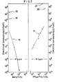
- Fig. 2 is a graph showing the electrical conductivity of the silicon thin films according to this invention as a function of the concentration of dopant gas.
- the curves 16 and 17 show the electrical conductivity of the P type and N type silicon thin films, respectively, produced by the conventional method, in which the films were formed at a cathode plasma discharge power density (fed plasma discharge power/area of cathode electrode) of about 0.1W/cm 2 .
- the points 18 and 19 shows the electrical conductivity of the P type silicon thin films produced by the method of this invention, in which the silane SiH 4 was diluted with hydrogen at ratio of silane to hydrogen of 1:30, and 2% by volume of diborane B 2 H 6 to silane was added to the gas mixture while plasma discharge power densities of 0.8W/cm 2 and 1.6 W/ cm 2 , respectively were employed.
- FIG. 2 shows the conductivity of the N type silicon thin films produced by the method of this invention, in which silane was diluted with hydrogen at a ratio of silane to hydrogen of 1:10, and for the point 20, 1% by volume of phosphorus pentafluoride PF 5 , and for the point 21, 4500 ppm by voluaae of phosphine PH 3 were added while power densities of 0.8W/cm 2 and 1.6W/cm , respectively were used. It proves from Fig. 2 that the conductivity of the silicon thin films of this invention is increased at least by two orders of magnitude in comparison with those produced by the conventional method.
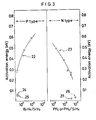
- Fig. 3 shows the activation energy on the basis of the electrical conductivity of the films of this invention as a function of the concentration of dopant gas.
- the curves 22 and 23 in Fig. 3 represent the activation energy of the films produced by the conventional method, in which the film forming conditions corresponding to the curves 16 and 17 in Fig. 2 were used, respectively.
- the points 24, 25, 26 and 27 represent the activation energy of the films produced by this invention, in which the film forming conditions corresponding to the 18, 19, 20 and 21 were used, respectively.
- Fig. 3 substantiates that this invention provides a P + type or N type film having a sufficiently low activation energy on the basis of electrical conductivity a good ohmic contact to metal, and an adequately degenerated Fermic level.
- Fig. 4 is a graph showing the concentrations of boron and phosphorus in the silicon thin films of this invention as a function of the concentration of dopant gas, as measured by the SIMS and EDMA methods.
- the curves 28 and 29 represent the films produced by the conventional method, in which the film forming conditions corresponding to the curves 16 and 17 in Fig. 2 were used.
- the points 30, 31, 32 and 33 in Fig. 4 represent the films produced by the method of this invention, in which the film forming conditions corresponding to the points 18, 19, 20 and 21 in Fig. 2 were used, respectively.
- Fig. 5 shows the optical band gap of the P type silicon thin film of this invention as a function of the concentration of dopant gas.
- the optical band gap is calculated on the basis of (h Y -E o ), wherein represents the absorption coefficient, h, the incident photon energy (eV), and E o , the optical band gap.
- the curve 34 in Fig. 5 is related to the film produced by the conventional method, in which the film forming conditions corresponding to the curve 16 in Fig. 2 were used. It shows that as the concentration of boron increases, the optical band gap decreases.
- the points 35 and 36 are concerned with the silicon films of this invention, in which the film forming condition corresponding to the points 18 and 19 in Fig. 2 were employed, respectively.
- Fig. 5 shows that the P type silicon thin film of thia invention has a high electrical conductivity without the optical band gap being narrowed.
- Fig. 6 shows an example of X ray (CuKa) diffraction pattern of the silicon thin film of this invention (having a film thickness of lpm).
- the curve 37 in Fig. 6 is a representative example of the sample of the invention, in which peaks are observed near Si (111) and Si (220). The grain diameter is calculated from the half-value width of peak to be about 100 i.
- the curve 38 in Fig. 6 represents the silicon thin film produced by the conventional method, in which no peak is observed unlike the curve 37. Further, the holo pattern appearing in this Figure is due to the glass material as a substrate, and holo pattern from the amorphous silicon film is not clearly observed, since the film is thin.
- a P type and N type silicon thin film having a high doping effect and a high electrical conductivity which have a wide application.
- P type silicon thin film is useful for solar cells and the like, since it can provide a high electrical conductivity without the optical band gap being narrowed.
- this invention has great advantages when used in the electronical industries.
Landscapes
- Chemical & Material Sciences (AREA)
- Inorganic Chemistry (AREA)
- General Chemical & Material Sciences (AREA)
- Chemical Kinetics & Catalysis (AREA)
- Engineering & Computer Science (AREA)
- Materials Engineering (AREA)
- Mechanical Engineering (AREA)
- Metallurgy (AREA)
- Organic Chemistry (AREA)
- Photovoltaic Devices (AREA)
- Silicon Compounds (AREA)
- Chemical Vapour Deposition (AREA)
Abstract
Applications Claiming Priority (2)
| Application Number | Priority Date | Filing Date | Title |
|---|---|---|---|
| JP55143010A JPS5767020A (en) | 1980-10-15 | 1980-10-15 | Thin silicon film and its manufacture |
| JP143010/80 | 1980-10-15 |
Publications (3)
| Publication Number | Publication Date |
|---|---|
| EP0062079A1 true EP0062079A1 (fr) | 1982-10-13 |
| EP0062079A4 EP0062079A4 (fr) | 1984-02-16 |
| EP0062079B1 EP0062079B1 (fr) | 1986-09-03 |
Family
ID=15328842
Family Applications (1)
| Application Number | Title | Priority Date | Filing Date |
|---|---|---|---|
| EP81902820A Expired EP0062079B1 (fr) | 1980-10-15 | 1981-10-15 | Film mince de silicium et procede de preparation |
Country Status (5)
| Country | Link |
|---|---|
| US (1) | US5017308A (fr) |
| EP (1) | EP0062079B1 (fr) |
| JP (1) | JPS5767020A (fr) |
| CA (1) | CA1175583A (fr) |
| WO (1) | WO1982001441A1 (fr) |
Cited By (8)
| Publication number | Priority date | Publication date | Assignee | Title |
|---|---|---|---|---|
| FR2561666A1 (fr) * | 1984-03-26 | 1985-09-27 | Agency Ind Science Techn | Procede de formation d'un film de silicium sur un substrat dans une atmosphere de plasma |
| EP0189636A1 (fr) * | 1984-11-02 | 1986-08-06 | Energy Conversion Devices, Inc. | Alliages semi-conducteurs microcristallins fluorés de type p et méthode de fabrication |
| EP0153043A3 (fr) * | 1984-02-15 | 1986-09-24 | Energy Conversion Devices, Inc. | Couche de contact ohmique |
| EP0262980A3 (en) * | 1986-10-03 | 1989-01-25 | Dow Corning Corporation | Method of forming semiconducting amorphous silicon films from the thermal decomposition of dihalosilanes |
| EP0344863A1 (fr) * | 1988-05-30 | 1989-12-06 | Interuniversitair Microelektronica Centrum Vzw | Procédé pour fabriquer un transistor à film mince |
| EP0592227A3 (fr) * | 1992-10-07 | 1995-01-11 | Sharp Kk | Fabrication d'un transistor à couche mince et production d'un dispositif d'affichage à cristaux liquides. |
| US5796116A (en) * | 1994-07-27 | 1998-08-18 | Sharp Kabushiki Kaisha | Thin-film semiconductor device including a semiconductor film with high field-effect mobility |
| US6078059A (en) * | 1992-07-10 | 2000-06-20 | Sharp Kabushiki Kaisha | Fabrication of a thin film transistor and production of a liquid display apparatus |
Families Citing this family (29)
| Publication number | Priority date | Publication date | Assignee | Title |
|---|---|---|---|---|
| JPS5939713A (ja) * | 1982-08-29 | 1984-03-05 | Agency Of Ind Science & Technol | シリコン薄膜及びその製造方法 |
| JPS61214475A (ja) * | 1985-03-19 | 1986-09-24 | Agency Of Ind Science & Technol | 薄膜トランジスタ |
| JPH0637703B2 (ja) * | 1986-12-22 | 1994-05-18 | 三井東圧化学株式会社 | 半導体薄膜の製法 |
| JP2516964B2 (ja) * | 1987-03-31 | 1996-07-24 | 鐘淵化学工業株式会社 | 歪センサ− |
| US4937550A (en) * | 1987-03-31 | 1990-06-26 | Kanegafuchi Kagaku Kogyo Kabushiki Kaisha | Strain sensor |
| JPH0351971Y2 (fr) * | 1988-05-12 | 1991-11-08 | ||
| JP2679354B2 (ja) * | 1990-04-13 | 1997-11-19 | 松下電器産業株式会社 | 非線形光学材料およびその製造方法 |
| US7154147B1 (en) * | 1990-11-26 | 2006-12-26 | Semiconductor Energy Laboratory Co., Ltd. | Electro-optical device and driving method for the same |
| US8106867B2 (en) | 1990-11-26 | 2012-01-31 | Semiconductor Energy Laboratory Co., Ltd. | Electro-optical device and driving method for the same |
| JPH04299578A (ja) * | 1991-03-27 | 1992-10-22 | Canon Inc | 光電変換素子及び薄膜半導体装置 |
| WO1993017449A1 (fr) * | 1992-02-25 | 1993-09-02 | Energy Conversion Devices, Inc. | Semiconducteur comportant des amas ordonnes et procede d'ablation au laser servant a sa fabrication |
| US5776819A (en) * | 1992-05-05 | 1998-07-07 | Midwest Research Institute | Deposition of device quality, low hydrogen content, amorphous silicon films by hot filament technique using "safe" silicon source gas |
| JPH0697070A (ja) * | 1992-09-11 | 1994-04-08 | Sanyo Electric Co Ltd | 多結晶シリコン膜の製造方法 |
| US5677236A (en) * | 1995-02-24 | 1997-10-14 | Mitsui Toatsu Chemicals, Inc. | Process for forming a thin microcrystalline silicon semiconductor film |
| US5885884A (en) * | 1995-09-29 | 1999-03-23 | Intel Corporation | Process for fabricating a microcrystalline silicon structure |
| ATE332572T1 (de) | 1996-06-19 | 2006-07-15 | Matsushita Electric Industrial Co Ltd | Photoelektronisches material, dieses verwendende vorrichtungen und herstellungsverfahren |
| US6087580A (en) * | 1996-12-12 | 2000-07-11 | Energy Conversion Devices, Inc. | Semiconductor having large volume fraction of intermediate range order material |
| EP1060287B1 (fr) * | 1998-03-06 | 2005-01-26 | ASM America, Inc. | Procede de depot de silicium, a pouvoir couvrant eleve |
| JP2000077402A (ja) * | 1998-09-02 | 2000-03-14 | Tokyo Electron Ltd | プラズマ処理方法および半導体装置 |
| JP4450126B2 (ja) * | 2000-01-21 | 2010-04-14 | 日新電機株式会社 | シリコン系結晶薄膜の形成方法 |
| US20040007733A1 (en) * | 2002-06-26 | 2004-01-15 | Macronix International Co., Ltd. | Floating gate memory cell and forming method |
| US20040209467A1 (en) * | 2003-04-21 | 2004-10-21 | Sinclair Wang | Method for reducing plasma related damages |
| US6872972B2 (en) * | 2003-07-16 | 2005-03-29 | Macronix International Co., Ltd. | Method for forming silicon film with changing grain size by thermal process |
| JP4489750B2 (ja) * | 2006-12-06 | 2010-06-23 | 株式会社半導体エネルギー研究所 | シリコン膜の作製方法、半導体装置の作製方法及び光電変換装置の作製方法 |
| US8535760B2 (en) * | 2009-09-11 | 2013-09-17 | Air Products And Chemicals, Inc. | Additives to silane for thin film silicon photovoltaic devices |
| WO2011142443A1 (fr) * | 2010-05-14 | 2011-11-17 | Semiconductor Energy Laboratory Co., Ltd. | Film de silicium microcristallin, procédé de fabrication de ce film, dispositif à semi-conducteur et procédé de fabrication de ce dispositif |
| US9443730B2 (en) | 2014-07-18 | 2016-09-13 | Asm Ip Holding B.V. | Process for forming silicon-filled openings with a reduced occurrence of voids |
| US9837271B2 (en) | 2014-07-18 | 2017-12-05 | Asm Ip Holding B.V. | Process for forming silicon-filled openings with a reduced occurrence of voids |
| US10460932B2 (en) | 2017-03-31 | 2019-10-29 | Asm Ip Holding B.V. | Semiconductor device with amorphous silicon filled gaps and methods for forming |
Family Cites Families (4)
| Publication number | Priority date | Publication date | Assignee | Title |
|---|---|---|---|---|
| DE2508802A1 (de) * | 1975-02-28 | 1976-09-09 | Siemens Ag | Verfahren zum abscheiden von elementarem silicium |
| US4226898A (en) * | 1978-03-16 | 1980-10-07 | Energy Conversion Devices, Inc. | Amorphous semiconductors equivalent to crystalline semiconductors produced by a glow discharge process |
| JPS56122123A (en) * | 1980-03-03 | 1981-09-25 | Shunpei Yamazaki | Semiamorphous semiconductor |
| JPS57160174A (en) * | 1981-03-30 | 1982-10-02 | Hitachi Ltd | Thin film solar battery |
-
1980
- 1980-10-15 JP JP55143010A patent/JPS5767020A/ja active Granted
-
1981
- 1981-10-14 CA CA000387901A patent/CA1175583A/fr not_active Expired
- 1981-10-15 WO PCT/JP1981/000286 patent/WO1982001441A1/fr not_active Ceased
- 1981-10-15 EP EP81902820A patent/EP0062079B1/fr not_active Expired
-
1989
- 1989-07-11 US US07/377,985 patent/US5017308A/en not_active Expired - Fee Related
Cited By (10)
| Publication number | Priority date | Publication date | Assignee | Title |
|---|---|---|---|---|
| EP0153043A3 (fr) * | 1984-02-15 | 1986-09-24 | Energy Conversion Devices, Inc. | Couche de contact ohmique |
| FR2561666A1 (fr) * | 1984-03-26 | 1985-09-27 | Agency Ind Science Techn | Procede de formation d'un film de silicium sur un substrat dans une atmosphere de plasma |
| EP0189636A1 (fr) * | 1984-11-02 | 1986-08-06 | Energy Conversion Devices, Inc. | Alliages semi-conducteurs microcristallins fluorés de type p et méthode de fabrication |
| EP0262980A3 (en) * | 1986-10-03 | 1989-01-25 | Dow Corning Corporation | Method of forming semiconducting amorphous silicon films from the thermal decomposition of dihalosilanes |
| EP0344863A1 (fr) * | 1988-05-30 | 1989-12-06 | Interuniversitair Microelektronica Centrum Vzw | Procédé pour fabriquer un transistor à film mince |
| US6078059A (en) * | 1992-07-10 | 2000-06-20 | Sharp Kabushiki Kaisha | Fabrication of a thin film transistor and production of a liquid display apparatus |
| EP0592227A3 (fr) * | 1992-10-07 | 1995-01-11 | Sharp Kk | Fabrication d'un transistor à couche mince et production d'un dispositif d'affichage à cristaux liquides. |
| US5686349A (en) * | 1992-10-07 | 1997-11-11 | Sharp Kabushiki Kaisha | Fabrication of a thin film transistor and production of a liquid crystal display apparatus |
| US5796116A (en) * | 1994-07-27 | 1998-08-18 | Sharp Kabushiki Kaisha | Thin-film semiconductor device including a semiconductor film with high field-effect mobility |
| US6271062B1 (en) | 1994-07-27 | 2001-08-07 | Sharp Kabushiki Kaisha | Thin film semiconductor device including a semiconductor film with high field-effect mobility |
Also Published As
| Publication number | Publication date |
|---|---|
| EP0062079B1 (fr) | 1986-09-03 |
| WO1982001441A1 (fr) | 1982-04-29 |
| JPS5767020A (en) | 1982-04-23 |
| CA1175583A (fr) | 1984-10-02 |
| EP0062079A4 (fr) | 1984-02-16 |
| JPS6356172B2 (fr) | 1988-11-07 |
| US5017308A (en) | 1991-05-21 |
Similar Documents
| Publication | Publication Date | Title |
|---|---|---|
| EP0062079B1 (fr) | Film mince de silicium et procede de preparation | |
| US4409605A (en) | Amorphous semiconductors equivalent to crystalline semiconductors | |
| US4226898A (en) | Amorphous semiconductors equivalent to crystalline semiconductors produced by a glow discharge process | |
| US4598164A (en) | Solar cell made from amorphous superlattice material | |
| CA1189601A (fr) | Dispositif photovoltaique aux caracteristiques courant ameliorees | |
| US4400409A (en) | Method of making p-doped silicon films | |
| EP0306297B1 (fr) | Dispositif photovoltaique à jonction pin dans lequel la couche semiconductrice de type I est constitueé de ZnSe ou ZnSeTe contenent de l'hydrogenedans une proportion atomique de 1 à 4% | |
| US4490208A (en) | Method of producing thin films of silicon | |
| JPS58199710A (ja) | 改良された広いバンドギヤツプのp型無定形の酸素とのシリコン合金およびその利用デバイス | |
| US4520380A (en) | Amorphous semiconductors equivalent to crystalline semiconductors | |
| CA1299716C (fr) | Element photovoltaique a jonction pin a couche de semiconducteur de type p ou n comportant un materiau non monocristallin contenant zn et se, ainsi que h dans un rapport atomique 1:4, monocristallin si(h,f) | |
| US4710786A (en) | Wide band gap semiconductor alloy material | |
| US4604636A (en) | Microcrystalline semiconductor method and devices | |
| US4446168A (en) | Method of forming amorphous silicon | |
| KR910002764B1 (ko) | 비결정 반도체의 제법 및 장치 | |
| JP2692091B2 (ja) | 炭化ケイ素半導体膜およびその製造方法 | |
| KR840002468B1 (ko) | 실리콘 함유층의 제조 공정 | |
| US4839312A (en) | Fluorinated precursors from which to fabricate amorphous semiconductor material | |
| JPS6329821B2 (fr) | ||
| US4703336A (en) | Photodetection and current control devices | |
| JPH03219622A (ja) | シリコン薄膜及びその製造方法 | |
| JPH03145719A (ja) | シリコン薄膜及びその製造方法 | |
| JPH02275620A (ja) | N型シリコン薄膜 | |
| Mochizuki et al. | Growth of CdTe thin films by direct reaction of Cd and Te vapors under hydrogen flow | |
| JPS6316616A (ja) | シリコン薄膜およびその製造方法 |
Legal Events
| Date | Code | Title | Description |
|---|---|---|---|
| PUAI | Public reference made under article 153(3) epc to a published international application that has entered the european phase |
Free format text: ORIGINAL CODE: 0009012 |
|
| AK | Designated contracting states |
Designated state(s): DE FR GB NL |
|
| 17P | Request for examination filed |
Effective date: 19821004 |
|
| GRAA | (expected) grant |
Free format text: ORIGINAL CODE: 0009210 |
|
| AK | Designated contracting states |
Kind code of ref document: B1 Designated state(s): DE FR GB NL |
|
| REF | Corresponds to: |
Ref document number: 3175268 Country of ref document: DE Date of ref document: 19861009 |
|
| ET | Fr: translation filed | ||
| PLBE | No opposition filed within time limit |
Free format text: ORIGINAL CODE: 0009261 |
|
| STAA | Information on the status of an ep patent application or granted ep patent |
Free format text: STATUS: NO OPPOSITION FILED WITHIN TIME LIMIT |
|
| 26N | No opposition filed | ||
| PGFP | Annual fee paid to national office [announced via postgrant information from national office to epo] |
Ref country code: NL Payment date: 19911031 Year of fee payment: 11 |
|
| PG25 | Lapsed in a contracting state [announced via postgrant information from national office to epo] |
Ref country code: NL Effective date: 19930501 |
|
| NLV4 | Nl: lapsed or anulled due to non-payment of the annual fee | ||
| PGFP | Annual fee paid to national office [announced via postgrant information from national office to epo] |
Ref country code: GB Payment date: 19941005 Year of fee payment: 14 |
|
| PGFP | Annual fee paid to national office [announced via postgrant information from national office to epo] |
Ref country code: DE Payment date: 19941010 Year of fee payment: 14 |
|
| PGFP | Annual fee paid to national office [announced via postgrant information from national office to epo] |
Ref country code: FR Payment date: 19941011 Year of fee payment: 14 |
|
| PG25 | Lapsed in a contracting state [announced via postgrant information from national office to epo] |
Ref country code: GB Effective date: 19951015 |
|
| GBPC | Gb: european patent ceased through non-payment of renewal fee |
Effective date: 19951015 |
|
| PG25 | Lapsed in a contracting state [announced via postgrant information from national office to epo] |
Ref country code: FR Effective date: 19960628 |
|
| PG25 | Lapsed in a contracting state [announced via postgrant information from national office to epo] |
Ref country code: DE Effective date: 19960702 |
|
| REG | Reference to a national code |
Ref country code: FR Ref legal event code: ST |