EP0062100A2 - Thyristor avec amplification de courant interne et procédé pour son fonctionnement - Google Patents
Thyristor avec amplification de courant interne et procédé pour son fonctionnement Download PDFInfo
- Publication number
- EP0062100A2 EP0062100A2 EP81108715A EP81108715A EP0062100A2 EP 0062100 A2 EP0062100 A2 EP 0062100A2 EP 81108715 A EP81108715 A EP 81108715A EP 81108715 A EP81108715 A EP 81108715A EP 0062100 A2 EP0062100 A2 EP 0062100A2
- Authority
- EP
- European Patent Office
- Prior art keywords
- emitter
- auxiliary emitter
- base
- thyristor
- semiconductor
- Prior art date
- Legal status (The legal status is an assumption and is not a legal conclusion. Google has not performed a legal analysis and makes no representation as to the accuracy of the status listed.)
- Granted
Links
Images


Classifications
-
- H—ELECTRICITY
- H10—SEMICONDUCTOR DEVICES; ELECTRIC SOLID-STATE DEVICES NOT OTHERWISE PROVIDED FOR
- H10D—INORGANIC ELECTRIC SEMICONDUCTOR DEVICES
- H10D62/00—Semiconductor bodies, or regions thereof, of devices having potential barriers
- H10D62/10—Shapes, relative sizes or dispositions of the regions of the semiconductor bodies; Shapes of the semiconductor bodies
- H10D62/17—Semiconductor regions connected to electrodes not carrying current to be rectified, amplified or switched, e.g. channel regions
- H10D62/192—Base regions of thyristors
- H10D62/206—Cathode base regions of thyristors
-
- H—ELECTRICITY
- H10—SEMICONDUCTOR DEVICES; ELECTRIC SOLID-STATE DEVICES NOT OTHERWISE PROVIDED FOR
- H10D—INORGANIC ELECTRIC SEMICONDUCTOR DEVICES
- H10D18/00—Thyristors
- H10D18/221—Thyristors having amplifying gate structures, e.g. cascade configurations
-
- H—ELECTRICITY
- H10—SEMICONDUCTOR DEVICES; ELECTRIC SOLID-STATE DEVICES NOT OTHERWISE PROVIDED FOR
- H10D—INORGANIC ELECTRIC SEMICONDUCTOR DEVICES
- H10D84/00—Integrated devices formed in or on semiconductor substrates that comprise only semiconducting layers, e.g. on Si wafers or on GaAs-on-Si wafers
- H10D84/101—Integrated devices comprising main components and built-in components, e.g. IGBT having built-in freewheel diode
- H10D84/131—Thyristors having built-in components
- H10D84/138—Thyristors having built-in components the built-in components being FETs
Definitions
- the invention relates to a thyristor with internal current amplification according to the preamble of claim 1 and to methods for its operation.
- a thyristor of this type is known from the "Thyristor Manual" by A. Hoffmann and K. Stokker, Verlag Siemens AG, Berlin and Kunststoff, 1965, pages 27 and 28.
- a current flows through the auxiliary emitter, which is referred to there as an intermediate grid, which causes rapid and large-scale firing in the area of the main emitter.
- a thyristor of this type is suitable for high rates of rise in the load current flowing between the anode and cathode, i.e. H. it has a high di / dt strength.
- German patent application P 29 45 347.2 describes a thyristor with internal current amplification, in which the main emitter has a plurality of fixed emitter short circuits, while the auxiliary emitter is provided with emitter short circuits, which can optionally be switched effectively by means of FET structures, i.e. H. are controllable. If they are activated, the thyristor has good stability, i. H. a high level of security against unintentional ignition processes when forward polarized voltages occur, which under certain circumstances can increase very quickly, i. H. represent a high dU / dt load. On the other hand, the thyristor is sensitive to ignition when the short circuits are ineffective.
- the advantage that can be achieved with the invention is in particular that the switchable auxiliary emitter is ineffective on the one hand in the non-conductive state of the semiconductor switch and does not reduce the stability of the thyristor, while on the other hand it significantly increases the ignition sensitivity of the thyristor in the conductive state of the semiconductor switch.
- the ignition sensitivity increases to the extent that the current amplification factor of the structure, which comprises the connectable auxiliary emitter and the two base layers, is greater with respect to the charge carriers emitted by the connectable auxiliary emitter than the corresponding current amplification factor of the structure, which comprises the auxiliary emitter and the two base layers .
- Claims 2 to 11 are directed to preferred refinements and developments of the invention, while claims 12 and 13 indicate advantageous methods for operating the thyristor according to the invention.
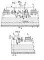
- a thyristor is shown, the one made of doped semiconductor material, for. B. silicon, existing semiconductor body with four layers of alternating conductivity types.
- the n-type layer 1 is referred to as the n-emitter, the p-type layer 2 as the p-base, the n-type layer 3 as the n-base and the p-type layer 4 as the p-type emitter .
- the p-emitter 4 is provided with an anode 5, which has a connection A, while the n-emitter 1 has a cathode 6 with a connection K.
- the n-emitter 1, ' which is the main emitter is penetrated by a plurality of lugs 7 of the p-base 2, extending up to the interface 8 of the semiconductor body and are conductively connected to the cathode in this. 6
- the approaches 7 represent so-called fixed emitter short circuits, which largely prevent an unintentional ignition of the thyristor when a blocking voltage is applied to the connections A and K, which places the anode 5 at a more positive potential than the cathode 6. This is explained by the fact that the defect electrons transported under the influence of the blocking voltage in the direction of the n-emitter 1 largely do not lead to the pn junction between parts 1 and.
- the thyristor is also insensitive to ignition, ie stable, with respect to larger or rapidly increasing blocking voltages at the connections A, K.
- n-type region 9, which represents the auxiliary emitter is inserted into the p-base 2 so that it extends to the interface 8.
- an auxiliary emitter electrode 10 contacts it, which conductively bridges the pn junction between the region 9 and the p base 2 in the direction of the n emitter 1.
- n-type region 11 extends starting from from the interface 8, much deeper into the P base 2 than the n-emitter 1 and the auxiliary emitter 9 and is produced by diffusion or implantation and subsequent driving of donors into the p-base 2. It is arranged laterally next to the auxiliary emitter 9, there being a distance from this which is determined by the width of a region 12 of the p-base 2.
- the area 12 is covered by a metallic or polysilicon gate 13 which is covered by a thin, electrically insulating layer 14, e.g. B. Si0 21 is separated from the interface 8.
- the gate 13 is connected to a control voltage socket 15.
- the mutually facing edge regions of the auxiliary emitter 9 and the region 11 together with the region 12, the insulating layer 14 and the gate 13 form a field effect transistor of the enhancement type.
- a control voltage which is positive in relation to K and exceeds the value of the threshold voltage is applied to the connection 15, an inversion channel is formed at the interface 8 below 13, which is indicated by 16.
- This n-conducting channel represents a low-resistance connection between regions 9 and 11. If the control voltage from terminal 15 is switched off, channel 16 is eliminated and the connection between regions 9 and 11 is interrupted.
- the structure formed from parts 9 to 16 thus represents a semiconductor switch which, in a first switching state, connects region 11 with low resistance to auxiliary emitter 9, so that an enlarged auxiliary emitter 9, 11 is formed, while in a second switching state, region 11 of isolates the auxiliary emitter 9 so that 11 cannot perform an auxiliary emitter function.
- area 11 is referred to as a switchable auxiliary emitter.
- the depth of penetration of the switchable express emitter 11 into the p-base 2 in the embodiment shown in FIG. 1 is more than twice the penetration depth of the express emitter 9 or that of the n-emitter 1. If one assumes a penetration depth of approximately 20 ⁇ m for the auxiliary emitter 9, the penetration depth of 11 is, for example, 50 ⁇ m. Accordingly, the distance D1 of the switchable auxiliary emitter 11 from the pn junction between the base layers 2 and 3 is smaller than the distance D2 of the auxiliary emitter 9 or the n-emitter 1 from this transition.
- the ignition of the thyristor according to FIG. 1 is explained below. It is assumed that a voltage that poles the thyristor in the forward direction is present at connections A and K and that a positive control voltage is supplied to connection 15. Under the influence of the first-mentioned voltage, for example, thermally generated defect electrons move along the path 1-7 shown in FIG. 1 in the direction of a fixed emitter short circuit 7, so that a voltage drop occurs at conductive channel 16 at point 18, which causes the pn junction between the connected auxiliary emitter 11 and the p-base 2 so far in the forward direction that electrons are emitted into the p-base 2 at this point.
- the electrons emitted by 11 move in the direction of the arrow 19, some of them the interface between reached the n-base 3 and the p-emitter 4 and caused an emission of defect electrons from the p-emitter. These emission processes mutually increase until layers 2 and 3 are flooded with emitted charge carriers, i. H. the thyristor has ignited in the area of the switchable auxiliary emitter 11.
- the load current flowing from A via the auxiliary emitter 9, 11 and the auxiliary emitter electrode 10 to the n-emitter 1 and to the cathode 6 represents a large ignition current for the n-emitter 1.
- the load current flowing between A and K becomes completely taken over by the part of the thyristor cross section which contains the ignited part of the n-emitter 1.
- the auxiliary emitter 9 is then no longer flowed through by the load current.
- a pulse-shaped control voltage P1 can thus be supplied to the connection 15, which is switched off when the thyristor cross section has become live in the area of the n-emitter 1.
- the thyristor is fired at lower voltages between A and K than was assumed in the above considerations, by means of an ignition current pulse P2, which is connected to an ignition circuit connected to 21 is fed.
- the bias voltage at the circuit point 18 is generated here by defect electrons which come from the semiconductor region below the ignition electrode 20 and reach a fixed short circuit 7 via the paths 17a and 17 shown in FIG. 1.
- the terminal 15 is connected to the control voltage P1 at the same time. Conveniently, the terminals 15 and 21 connected to each other, wherein the ignition current pulse P2 from the terminal 15 the voltage pulse P1 - drops.
- the thyristor is extinguished when the load current falls below a so-called holding current. This happens, for example, when the voltage from terminals A and K is switched off, or, if it is an AC voltage, when the next zero crossing occurs.
- the current amplification factor ⁇ npn1 of the npn structure formed from parts 11, 2 and 3, which refers to the electrons emitted by 11 is significantly larger than the current amplification factor ⁇ npn2 for the npn structure formed from parts 9, 2 and 3. This can be explained from the fact that the recombination rate of the electrons emitted by 9 is substantially greater than the recombination rate of the electrons emitted by 11 because of the greater distance D2 of the auxiliary emitter 9 from the interface between 2 and 3.
- the ignition sensitivity of the thyristor according to FIG. 1 is therefore greater than the ignition sensitivity of a conventional thyristor with internal ignition amplification, as the current amplification factor ⁇ npn1 is greater than ⁇ npn2 .
- the p-base 2 has a doping profile in which the degree of doping in the region of the lower boundary surface of the switchable auxiliary emitter 11 is smaller than on the lower boundary surface of the auxiliary emitter 9, then the prestress of the pn junction between the semiconductor parts 11 prevailing at point 18 becomes and 2 compared to the case in which the degree of doping of the p base does not have such a reduction, so that the ignition sensitivity in the region of the switchable auxiliary emitter 11 increases further.
- FIG. 1 If one now starts in FIG. 1 from a rotationally symmetrical structure of the thyristor with the line 22 as an axis of symmetry, there are annular configurations of parts 1, 9, 11, 6, 10 and 13. The sectional areas of these parts which are to the left of 22 , are designated 1 ', 9', 11 ', 6', 10 'and 13'. Such a structure is ignited along a circle concentric to axis 22, which contains points 18 and 18 '.
- line 22 in FIG. 1 can also be drawn up as a plane of symmetry perpendicular to the image plane be caught.
- the parts 1, 9, 11; 6, 10 and 13 expediently have an elongated shape and, with their larger dimensions, run perpendicular to the plane of the drawing, preferably over the entire thyristor cross section.
- Parts 1 ', 9', 11 ', 6', 10 'and 13' then represent analog partial structures on the other side of the plane of symmetry, which are symmetrical with respect to the latter with respect to parts 1, 9, 11, 6, 10 and 13 lie.
- the gates 13 and 13 ' are connected to one another for the purpose of a common control, which is indicated by a line 23 shown in the drawing, and can be connected to the connection 21.
- the cathode 6 ' is connected to the cathode 6, which is indicated by a line 24.
- the parts 1, 9, 11, 6, 10 and 13 can advantageously also be strip-shaped and cover the thyristor cross section or parts thereof in the form of a spiral or the like.
- a switchable auxiliary emitter 25 is provided which takes the place of the switchable auxiliary emitter 11 of FIG. 1 and has the same external dimensions as the p base 2 as this. It is provided on the edge zones of a trench-shaped recess 26 of the p-base 2, with it starting from the edge of the same only a few ⁇ m, for. B. 5 microns, extends deep into the p-base 2.
- the n-type region 25 is produced by diffusion or implantation of donors, while the recess 26 is preferably produced by etching.
- the other circuit parts of FIG. 2 correspond to the same-named circuit parts of FIG. 1.
- FIG. 3 shows a thyristor with a p-emitter 27, an n-base 28 and a p-base 29.
- An auxiliary emitter 30 and a switchable auxiliary emitter 31 replace parts 9 and 11 of FIG. 1 and have the same lateral dimensions compared to that p-base 29 on parts 9 and 11 with respect to p-base 2.
- 32 denotes an n-emitter, which takes the place of the n-emitter 1 from FIG. 1 and has the same lateral dimensions as this.
- the vertical dimensions of the parts 30 to 32 are matched to one another, wherein they are expediently larger than the vertical dimension of the n-emitter 1 and, for example, correspond to those of the parts 11 and 11 'in FIG. 1.
- the other circuit parts of FIG. 3 correspond to the circuit parts of FIG. 1 provided with the same reference symbols.
- the n-emitter 32 and the auxiliary emitter 30 are surrounded by a partial region 33 of the p-base 29, which has an additional p-doping, so that its degree of doping is higher than that of the remaining partial regions of the p-base 29.
- the three-layer structure consisting of parts 30, 29 and 28 has a current amplification factor a n p n2 with respect to the electrons emitted in the case of a voltage of 30 at A and K in the forward direction of the thyristor, which is smaller than the corresponding one Current amplification factor a n p n1 of the three-layer structure 31, 29 and 28 with respect to the electrons emitted by the switchable auxiliary emitter 31.
- the terminal 15 is a control voltage, for. B. P1, which causes regions 30 and 31 to be connected to each other in a low-resistance manner via the inversion channel indicated by 16, the thyristor in region 31 is very sensitive to ignition.
- the control voltage from terminal 15 is switched off, the auxiliary emitter 31 is ineffective, so that the thyristor has great stability because of the fixed emitter short circuits 7 and the high doping of the partial region 33.
- an impurity concentration in the p-base 29 of approximately 5 ⁇ 10 16 cm -3
- an impurity concentration occurs for the partial region 33, for example Concentration of about 2 x 10 17 cm -3 into consideration, these figures only serve to explain the doping difference mentioned and are not to be interpreted as limit values.
- Different current amplification factors ⁇ npn1 and a n p n2 can also be achieved in such a way that the partial region 33 is not more heavily doped than the other parts of the p-emitter 29, but instead is provided with additional recombination centers. This happens e.g. B. by irradiating the p-base 29 to the partial region 33 before generating the regions 32 and 30 with an electron beam.
- recombination centers in the form of gold or platinum antibodies can also be introduced into the partial region 33 by diffusion or implantation. The increase in the number of recombination centers in partial area 33 results in a decrease in ⁇ npn2 compared to ⁇ npn1 .
- the thyristors according to FIGS. 2 and 3 are operated in the same way as the thyristor according to FIG. 1.
- the exemplary embodiment shown in FIG. 4 differs from FIG. 1 in that 7 controllable emitter short-circuits are provided instead of the fixed emitter short-circuits.
- the n-emitter 1 of FIG. 1 is divided into two or more emitter subregions 1a, 1b, each of which is provided with a part 6a or 6b of the cathode.
- the parts 6a and 6b are connected to one another and led to a common connection K.
- a controllable emitter short circuit designated SE 1 in FIG. 4, has a p-type semiconductor region 34 inserted into the emitter sub-region 1 a, which extends to the interface 8 of the semiconductor body and in which the part 6 a of the cathode contacts it.
- the emitter subregions 1a and 1b are through a region 35 the p base 2 separated from one another, which is to be understood as a second p-type semiconductor region of the controllable emitter short circuit.
- the latter is covered by a gate 37, which has a connection 38 and a thin, electrically insulating layer 39, for. B.
- the parts 34 to 37 form a FET structure of the depletion type, in which, without supplying a control voltage to the connection 38, there is a p-type channel 40 in the edge region 36 which defines the region 34 with the region 35 and thus the part 6a of the cathode connects to the p-base 2 with low resistance.
- the channel 40 is either an inversion channel or a doped channel generated by a p-doping at the interface 8.
- the emitter short-circuit SE1 is thus effectively switched when the connection 38 is voltage-free. If the connection 38 is supplied with a positive control voltage, the channel 40 is eliminated and the low-resistance connection of parts 2 and 6a is interrupted, ie the emitter short circuit SE1 is deactivated.
- FIG. 4 a further controllable emitter short-circuit SE2 is provided at the edge of the emitter sub-region 1b, which is constructed in accordance with SE1.
- the gate 37 is assigned to the emitter short circuits SE1 and SE2 together.
- a line designated 41 which connects the connections 38 and 15 to one another, is expediently provided.
- the connections 15 and 38 can also be connected individually or together to the connection 21.
- the other circuit parts in FIG. 4 correspond to the parts in FIG. 1 which have the same reference numerals
- E m itter subareas 1a and 1b can, in the embodiment of FIG. 4 also several correspondingly shaped emitter sub-regions, or even a single such sub-region, for. B. 1a or 1b.
- a particularly high stability is achieved with the exemplary embodiment according to FIG. 4, in particular when a larger number of emitter sub-regions 1a, 1b ... and a correspondingly large number of controllable emitter short-circuits SE1, SE2 ... are provided. These are caused by a positive control voltage, e.g. B. pulse-shaped control voltage P3, ineffective so that the spread of the ignited front is not hindered by the emitter short circuits over the entire thyristor cross section. If the thyristor cross in the area of E m itter subareas 1a, 1b become energized, the control voltage can be switched off, as indicated by P3. If a connection 21 is provided, to which an ignition current pulse P2 is supplied, connection 38 can be connected to 21 in order to be able to use the voltage dropping at 21 as control voltage P3. The connection 15 is controlled in the manner already shown in FIG. -1 explained way.
- the FET structures described so far, e.g. 34 to 40 of the depletion type can also be replaced by FET structures of the enhancement type if their gate connections, e.g. B. 38, an additional negative control voltage is supplied, the I n version channels, z. B. 40, arises.
- the control voltage P3 is then superimposed on this additional control voltage at the ignition point in order to cancel the channels.
- FIG. 5 shows another embodiment of the exemplary embodiment according to FIG. 1, in which the connectable auxiliary emitter 11 is conductively connected to the auxiliary emitter 9 via a semiconductor switch in the form of an external field effect transistor 42.
- the source-drain path of 42 is connected on the one hand to the auxiliary emitter electrode 10 and on the other hand to a conductive assignment 43, which contacts the switchable auxiliary emitter 11.
- the gate of 42 is provided with a control voltage connection 44 which can be connected to the connection 21 via a line 45.
- the operation of the thyristor according to FIG. 5 takes place in the manner described with reference to FIG. 1, the connection 44 corresponding to the connection 15 and being supplied with the control voltage P1, while an ignition current pulse P2 is optionally supplied to the connection 21.
- the switchable auxiliary emitter can also be p-conducting, arranged laterally next to the p-emitter in the n-base of the thyristor and connected to this p-emitter with a low resistance to produce a high ignition sensitivity via a semiconductor switch.
- the fixed or controllable emitter short-circuits are also provided in the area of the p-emitter. All of the figures can be used to illustrate this circuit variant if the names of the connections A and K are interchanged, the semiconductor parts each receive the opposite line types to those described so far, and the control voltages mentioned and the control current are supplied with opposite polarity.
- All of the exemplary embodiments according to FIGS. 2 to 5 can each be designed to be symmetrical about an axis of symmetry 22 corresponding to FIG. 1, or they can be constructed symmetrically to a plane that is perpendicular to the image plane and is indicated by 22.
- the exemplary embodiments according to FIGS. 2, 3 and 4 can also be equipped with a semiconductor switch in the form of an external transistor.
- the switchable auxiliary emitters 11 of FIGS. 4 and 5 can be designed in accordance with parts 25, 26 of FIG. 2. and the fixed emitter shorts 7 in all figures by controllable emitter shorts, e.g. B. SE1 or SE2, to be replaced.
Landscapes
- Thyristors (AREA)
- Thyristor Switches And Gates (AREA)
Applications Claiming Priority (2)
| Application Number | Priority Date | Filing Date | Title |
|---|---|---|---|
| DE3112941 | 1981-03-31 | ||
| DE19813112941 DE3112941A1 (de) | 1981-03-31 | 1981-03-31 | Thyristor mit innerer stromverstaerkung und verfahren zu seinem betrieb |
Publications (3)
| Publication Number | Publication Date |
|---|---|
| EP0062100A2 true EP0062100A2 (fr) | 1982-10-13 |
| EP0062100A3 EP0062100A3 (en) | 1983-10-12 |
| EP0062100B1 EP0062100B1 (fr) | 1987-05-06 |
Family
ID=6128935
Family Applications (1)
| Application Number | Title | Priority Date | Filing Date |
|---|---|---|---|
| EP81108715A Expired EP0062100B1 (fr) | 1981-03-31 | 1981-10-22 | Thyristor avec amplification de courant interne et procédé pour son fonctionnement |
Country Status (4)
| Country | Link |
|---|---|
| US (1) | US4502072A (fr) |
| EP (1) | EP0062100B1 (fr) |
| JP (1) | JPS57170569A (fr) |
| DE (1) | DE3112941A1 (fr) |
Cited By (6)
| Publication number | Priority date | Publication date | Assignee | Title |
|---|---|---|---|---|
| EP0106059A1 (fr) * | 1982-08-18 | 1984-04-25 | Siemens Aktiengesellschaft | Commutateur semi-conducteur muni d'un thyristor à blocage par la gâchette |
| EP0108961A1 (fr) * | 1982-11-15 | 1984-05-23 | Kabushiki Kaisha Toshiba | Dispositif à thyristor protégé contre la surtension |
| DE3435548A1 (de) * | 1984-09-27 | 1986-04-03 | Siemens AG, 1000 Berlin und 8000 München | Thyristor mit hoher innerer zuendverstaerkung |
| EP0312088A3 (fr) * | 1987-10-16 | 1990-12-27 | Kabushiki Kaisha Toshiba | Thyristor sensible ayant une immunité au bruit améliorée |
| WO1997044827A1 (fr) * | 1996-05-20 | 1997-11-27 | Siemens Aktiengesellschaft | Thyristor a protection du/dt integree |
| DE19947028A1 (de) * | 1999-09-30 | 2001-04-12 | Siemens Ag | Thyristor mit Spannungsstoßbelastbarkeit in der Freiwerdezeit |
Families Citing this family (2)
| Publication number | Priority date | Publication date | Assignee | Title |
|---|---|---|---|---|
| US5082795A (en) * | 1986-12-05 | 1992-01-21 | General Electric Company | Method of fabricating a field effect semiconductor device having a self-aligned structure |
| DE3869752D1 (de) * | 1987-12-23 | 1992-05-07 | Bbc Brown Boveri & Cie | Abschaltbarer thyristor mit ueberspannungsschutz. |
Family Cites Families (18)
| Publication number | Priority date | Publication date | Assignee | Title |
|---|---|---|---|---|
| DE8008C (de) * | Dr. KIRSTEIN, prakt. Zahnarzt, in Berlin | Verfahren zur Herstellung künstlicher Gebisse aus natürlichen Zähnen in Celluloide-Gaumenplatten | ||
| NL129185C (fr) * | 1960-06-10 | |||
| NL293292A (fr) * | 1962-06-11 | |||
| US3300694A (en) * | 1962-12-20 | 1967-01-24 | Westinghouse Electric Corp | Semiconductor controlled rectifier with firing pin portion on emitter |
| SE311701B (fr) * | 1966-07-07 | 1969-06-23 | Asea Ab | |
| US3486088A (en) * | 1968-05-22 | 1969-12-23 | Nat Electronics Inc | Regenerative gate thyristor construction |
| SE320729B (fr) * | 1968-06-05 | 1970-02-16 | Asea Ab | |
| JPS51142983A (en) * | 1975-06-04 | 1976-12-08 | Hitachi Ltd | Scr |
| SE392783B (sv) * | 1975-06-19 | 1977-04-18 | Asea Ab | Halvledaranordning innefattande en tyristor och en felteffekttransistordel |
| JPS5933986B2 (ja) * | 1975-09-12 | 1984-08-20 | 三菱電機株式会社 | 半導体装置 |
| US4060825A (en) * | 1976-02-09 | 1977-11-29 | Westinghouse Electric Corporation | High speed high power two terminal solid state switch fired by dV/dt |
| JPS588033B2 (ja) * | 1976-08-20 | 1983-02-14 | 松下電器産業株式会社 | 車輛台数計数装置 |
| US4165517A (en) * | 1977-02-28 | 1979-08-21 | Electric Power Research Institute, Inc. | Self-protection against breakover turn-on failure in thyristors through selective base lifetime control |
| JPS6016107B2 (ja) * | 1978-08-23 | 1985-04-23 | 株式会社日立製作所 | 自己保護型半導体制御整流装置 |
| JPS5574168A (en) * | 1978-11-28 | 1980-06-04 | Oki Electric Ind Co Ltd | Pnpn switch |
| JPS55113371A (en) * | 1979-02-21 | 1980-09-01 | Shindengen Electric Mfg Co Ltd | Power transistor |
| DE2945347A1 (de) * | 1979-11-09 | 1981-05-21 | Siemens AG, 1000 Berlin und 8000 München | Thyristor mit hilfsemitterelektrode und verfahren zu seinem betrieb |
| DE2945335A1 (de) * | 1979-11-09 | 1981-06-04 | Siemens AG, 1000 Berlin und 8000 München | Lichtzuendbarer thyristor |
-
1981
- 1981-03-31 DE DE19813112941 patent/DE3112941A1/de not_active Ceased
- 1981-10-22 EP EP81108715A patent/EP0062100B1/fr not_active Expired
-
1982
- 1982-02-04 US US06/345,925 patent/US4502072A/en not_active Expired - Fee Related
- 1982-03-26 JP JP57048765A patent/JPS57170569A/ja active Granted
Cited By (8)
| Publication number | Priority date | Publication date | Assignee | Title |
|---|---|---|---|---|
| EP0106059A1 (fr) * | 1982-08-18 | 1984-04-25 | Siemens Aktiengesellschaft | Commutateur semi-conducteur muni d'un thyristor à blocage par la gâchette |
| EP0108961A1 (fr) * | 1982-11-15 | 1984-05-23 | Kabushiki Kaisha Toshiba | Dispositif à thyristor protégé contre la surtension |
| DE3435548A1 (de) * | 1984-09-27 | 1986-04-03 | Siemens AG, 1000 Berlin und 8000 München | Thyristor mit hoher innerer zuendverstaerkung |
| EP0312088A3 (fr) * | 1987-10-16 | 1990-12-27 | Kabushiki Kaisha Toshiba | Thyristor sensible ayant une immunité au bruit améliorée |
| WO1997044827A1 (fr) * | 1996-05-20 | 1997-11-27 | Siemens Aktiengesellschaft | Thyristor a protection du/dt integree |
| US6066864A (en) * | 1996-05-20 | 2000-05-23 | Siemens Aktiengesellschaft | Thyristor with integrated dU/dt protection |
| DE19947028A1 (de) * | 1999-09-30 | 2001-04-12 | Siemens Ag | Thyristor mit Spannungsstoßbelastbarkeit in der Freiwerdezeit |
| US6727526B1 (en) | 1999-09-30 | 2004-04-27 | Siemens Aktiengesellschaft | Thyristor with recovery time voltage surge resistance |
Also Published As
| Publication number | Publication date |
|---|---|
| EP0062100A3 (en) | 1983-10-12 |
| DE3112941A1 (de) | 1982-10-07 |
| EP0062100B1 (fr) | 1987-05-06 |
| US4502072A (en) | 1985-02-26 |
| JPS57170569A (en) | 1982-10-20 |
| JPH0138380B2 (fr) | 1989-08-14 |
Similar Documents
| Publication | Publication Date | Title |
|---|---|---|
| DE2625917C3 (de) | Halbleiteranordnung | |
| EP0106059B1 (fr) | Commutateur semi-conducteur muni d'un thyristor à blocage par la gâchette | |
| EP0028799B1 (fr) | Triac comportant un corps semiconducteur multi-couches et procédé pour son fonctionnement | |
| EP0030274B1 (fr) | Thyristor à courts-circuits d'émetteur contrôlables et procédé pour son fonctionnement | |
| EP0062099B1 (fr) | Thyristor et procédé pour son fonctionnement | |
| DE2945347C2 (fr) | ||
| DE1464983C2 (de) | in zwei Richtungen schaltbares und steuerbares Halbleiterbauelement | |
| EP0062100B1 (fr) | Thyristor avec amplification de courant interne et procédé pour son fonctionnement | |
| DE3018499C2 (fr) | ||
| EP0062102B1 (fr) | Thyristor avec amplification de courant interne commutable et procédé pour son fonctionnement | |
| WO1998012749A2 (fr) | Thyristor commande par emetteur | |
| EP0104390B1 (fr) | Thyristor commutable à l'état non conducteur | |
| EP0064715B1 (fr) | Thyristor avec courts-circuits d'émetteur contrôlables insérés dans l'émetteur | |
| DE4024526A1 (de) | Abschaltbares, mos-gesteuertes leistungshalbleiter-bauelement sowie verfahren zu dessen herstellung | |
| EP0065671B1 (fr) | Thyristor ayant une électrode d'émetteur auxiliaire et des régions en court-circuit et fonctionnement du thyristor | |
| DE69432111T2 (de) | Bipolartransistor mit isoliertem Gate | |
| EP0064716B1 (fr) | Triac et procédé pour son fonctionnement | |
| EP0064718B1 (fr) | Thyristor commandé par la lumière avec émetteur court-circuité contrôlé optoélectroniquement et procédé pour son fonctionnement | |
| EP0064719B1 (fr) | Thyristor commandé par la lumière avec courts-circuits d'émetteur contrôlables et procédé pour son fonctionnement | |
| DE4126491A1 (de) | Abschaltbares leistungshalbleiter-bauelement | |
| EP0075719A2 (fr) | Thyristor à émetteur en court-circuit contrôllable et à amorçage amplifié | |
| EP0137951A1 (fr) | Thyristor à émetteurs court-circuités commandé par une structure MIS | |
| DE3837747A1 (de) | Halbleiterschalter |
Legal Events
| Date | Code | Title | Description |
|---|---|---|---|
| PUAI | Public reference made under article 153(3) epc to a published international application that has entered the european phase |
Free format text: ORIGINAL CODE: 0009012 |
|
| 17P | Request for examination filed |
Effective date: 19811022 |
|
| AK | Designated contracting states |
Designated state(s): CH FR GB IT SE |
|
| PUAL | Search report despatched |
Free format text: ORIGINAL CODE: 0009013 |
|
| AK | Designated contracting states |
Designated state(s): CH FR GB IT LI SE |
|
| 17Q | First examination report despatched |
Effective date: 19860206 |
|
| GRAA | (expected) grant |
Free format text: ORIGINAL CODE: 0009210 |
|
| AK | Designated contracting states |
Kind code of ref document: B1 Designated state(s): CH FR GB IT LI SE |
|
| ET | Fr: translation filed | ||
| ITF | It: translation for a ep patent filed | ||
| PLBE | No opposition filed within time limit |
Free format text: ORIGINAL CODE: 0009261 |
|
| STAA | Information on the status of an ep patent application or granted ep patent |
Free format text: STATUS: NO OPPOSITION FILED WITHIN TIME LIMIT |
|
| 26N | No opposition filed | ||
| PGFP | Annual fee paid to national office [announced via postgrant information from national office to epo] |
Ref country code: GB Payment date: 19890930 Year of fee payment: 9 |
|
| PGFP | Annual fee paid to national office [announced via postgrant information from national office to epo] |
Ref country code: FR Payment date: 19891026 Year of fee payment: 9 |
|
| PGFP | Annual fee paid to national office [announced via postgrant information from national office to epo] |
Ref country code: SE Payment date: 19891027 Year of fee payment: 9 |
|
| ITTA | It: last paid annual fee | ||
| PGFP | Annual fee paid to national office [announced via postgrant information from national office to epo] |
Ref country code: CH Payment date: 19900124 Year of fee payment: 9 |
|
| PG25 | Lapsed in a contracting state [announced via postgrant information from national office to epo] |
Ref country code: GB Effective date: 19901022 |
|
| PG25 | Lapsed in a contracting state [announced via postgrant information from national office to epo] |
Ref country code: SE Effective date: 19901023 |
|
| PG25 | Lapsed in a contracting state [announced via postgrant information from national office to epo] |
Ref country code: LI Effective date: 19901031 Ref country code: CH Effective date: 19901031 |
|
| GBPC | Gb: european patent ceased through non-payment of renewal fee | ||
| PG25 | Lapsed in a contracting state [announced via postgrant information from national office to epo] |
Ref country code: FR Effective date: 19910628 |
|
| REG | Reference to a national code |
Ref country code: CH Ref legal event code: PL |
|
| REG | Reference to a national code |
Ref country code: FR Ref legal event code: ST |
|
| EUG | Se: european patent has lapsed |
Ref document number: 81108715.4 Effective date: 19910603 |