EP0062894B1 - Halbleiteranordnung - Google Patents
Halbleiteranordnung Download PDFInfo
- Publication number
- EP0062894B1 EP0062894B1 EP82102994A EP82102994A EP0062894B1 EP 0062894 B1 EP0062894 B1 EP 0062894B1 EP 82102994 A EP82102994 A EP 82102994A EP 82102994 A EP82102994 A EP 82102994A EP 0062894 B1 EP0062894 B1 EP 0062894B1
- Authority
- EP
- European Patent Office
- Prior art keywords
- semiconductor region
- semiconductor
- conductivity type
- region
- substrate
- Prior art date
- Legal status (The legal status is an assumption and is not a legal conclusion. Google has not performed a legal analysis and makes no representation as to the accuracy of the status listed.)
- Expired
Links
Images


Classifications
-
- G—PHYSICS
- G05—CONTROLLING; REGULATING
- G05F—SYSTEMS FOR REGULATING ELECTRIC OR MAGNETIC VARIABLES
- G05F3/00—Non-retroactive systems for regulating electric variables by using an uncontrolled element, or an uncontrolled combination of elements, such element or such combination having self-regulating properties
- G05F3/02—Regulating voltage or current
- G05F3/08—Regulating voltage or current wherein the variable is DC
- G05F3/10—Regulating voltage or current wherein the variable is DC using uncontrolled devices with non-linear characteristics
- G05F3/16—Regulating voltage or current wherein the variable is DC using uncontrolled devices with non-linear characteristics being semiconductor devices
- G05F3/20—Regulating voltage or current wherein the variable is DC using uncontrolled devices with non-linear characteristics being semiconductor devices using diode- transistor combinations
- G05F3/205—Substrate bias-voltage generators
-
- H—ELECTRICITY
- H10—SEMICONDUCTOR DEVICES; ELECTRIC SOLID-STATE DEVICES NOT OTHERWISE PROVIDED FOR
- H10D—INORGANIC ELECTRIC SEMICONDUCTOR DEVICES
- H10D89/00—Aspects of integrated devices not covered by groups H10D84/00 - H10D88/00
- H10D89/211—Design considerations for internal polarisation
- H10D89/213—Design considerations for internal polarisation in field-effect devices
- H10D89/215—Design considerations for internal polarisation in field-effect devices comprising arrangements for charge pumping or biasing substrates
Definitions
- the present invention relates to a semiconductor device with a self substrate bias generator.
- a self substrate bias generator which generates a voltage with an opposite polarity to that of a power source voltage externally supplied and supplies it to a substrate.
- a self substrate bias generator is formed on a semiconductor substrate.
- Fig. 1 shows an example of the self-substrate bias generator using the charge pumping effect.
- a circuit for generating an alternating voltage (referred to as a generating circuit) 10 grounded at one end generates an AC voltage oscillating between the reference voltage V ss and the power source voltage V DD .
- the other end of the generating circuit 10 is connected through a capacitor 12 for charge pumping to the source of an N channel MOS transistor 14.
- the gate and drain of the MOS transistor 14 are both connected to a terminal 16 connected to the substrate.
- a node between the generating circuit 10 and the capacitor 12 is denoted as N1 and the node between the source of the transistor 14 and the capacitor 12 is denoted as N2.
- the node N2 is connected to the gate and drain of an N channel MOS transistor 18 the source of which is grounded.
- the transistors 14 and 18 effect the rectification.
- the current rectified flows from the terminal 16 to ground through the node N2.
- the charge induced into the node N2 by means of the generating circuit 10 via the capacitor 12 is supplied from the terminal 16.
- the induced charge is discharged to ground through the transistor 18.
- a current flows from the terminal 16 to ground, so thatthe terminal (substrate) 16 is biased to a negative potential.
- FIG. 2 illustrates a structural diagram of the self substrate bias generator shown in Fig. 1.
- a P type high concentration impurity region 22 and N type high concentration impurity regions 24, 26 and 28 are formed on the surface region of a P type silicon substrate (corresponding to the terminal 16 in Fig. 1).
- a gate electrode 32 is formed on the silicon substrate 20 between the N type high concentration impurity regions 24 and 26, with a gate insulating film 30 interposed therebetween.
- Another gate electrode 36 is formed on the N type high concentration impurity region 28 through a gate insulating film 34.
- the capacitor 12 is made up of the gate electrode 36, the gate insulating film 34 and the N type high concentration impurity region 28.
- the region 26, the electrode 32 and the region 24 serve as the source, gate and drain of the MOS transistor 14, respectively.
- the impurity region 22 is a diffusion region for enhancing the ohmic contact with the silicon substrate 20.
- Other circuit elements such as a memory cell are formed on the P type silicon substrate 20.
- the prior self substrate bias generator has the following disadvantages.
- the potential at the impurity region 26 (corresponding to the node N2 in Fig. 1) changes with a variation of the output voltage from the generating circuit 10. Accordingly, the potential of the impurity region 26 falls possibly below that of the silicon substrate 20.
- the PN junction (corresponding to the diode 38 indicated by a broken line in Fig. 1) between the silicon substrate 20 and the high concentrated impurity region 26 is forwardly biased. Therefore, a large amount of electrons are injected into the silicon substrate 20. Since the life time of the minority carriers in the P type substrate are long, the carriers moves in the substrate to possibly enter the peripheral circuit elements, providing causes of an erroneous operation of the integrated circuit.
- the integrated circuit operating in a dynamic mode uses many modes in a floating state and hence is easily influenced by the minority carriers.
- the floating nodes are frequently used for reducing the power consumption of the integrated circuit.
- the circuit elements tend to erroneously operate.
- the holes enter the substrate to become the minority carriers, causing the erroneous operation of the circuit elements similarly.
- an object of the present invention is to provide a semiconductor device which can reduce the amount of the minority carriers injected from the self substrate bias generator into the semiconductor substrate.
- a semiconductor substrate of the first conductivity type in which a self substrate bias generator is formed is impressed with a reference potential to block the flow of the minority carriers from the self bias generator.
- a group of circuit elements impressed with a voltage generated by the self-substrate bias generator are formed in a semiconductor region of the second conductivity type formed in the semiconductor substrate.
- the amount of the minority carriers injected into the semiconductor substrate can be reduced.
- the erroneous operation of the circuit elements can be prevented to improve the reliability of the semiconductor device.
- JP-A-55 59757 JP-A-55 107 255 Other arrangements are known in the prior art (JP-A-55 59757 JP-A-55 107 255). However in these arrangements the injecting regions are surrounded with highly doped layers of the opposite conductivity type.
- the charge pumping efficiency of the self substrate bias generator can be improved.
- a semiconductor region of the second conductivity type is formed in the semiconductor substrate of the first conductivity type and the self substrate bias generator is formed in the semiconductor region, it is possible to prevent the minority carriers injected into the semiconductor region from diffusing into the peripheral region.
- Fig. 3 is a circuit diagram of a self substrate bias generator in a semiconductor device according to the present invention.
- An AC voltage generating circuit 110 connected at one end to ground produces an AC voltage oscillating between a reference voltage V ss (ground potential in this case) and a power source voltage V DD .
- the other end of the generating circuit 110 is connected to a terminal 116 through a capacitor 112 and a P channel MOS transistor 114.
- the terminal 116 is connected to a semiconductor region to be supplied with a voltage generated by the self substrate bias generator.
- a node between the generating circuit 110 and the capacitor 112 is denoted as N11 and a node between the drain of the transistor 114 and the capacitor 112 is denoted as N12.
- the node N12 is connected to the source of a P channel MOS transistor 118 grounded at the gate and drain.
- the gate of the transistor 114 is connected to the node N12.
- a power source voltage V DD is applied to the substrate regions in which the channel of the transistor 114 is formed and the channel of the transistor 118 is formed.
- the transistors 114 and 118 both have a rectification characteristic.
- the current flows, due to the charge pumping action, from the terminal 116 toward the node N12 and from the node N12 toward ground. Accordingly, the terminal 116 is biased to a negative potential.
- Fig. 4 illustrates, structurally and schematically, a semiconductor device with a self substrate bias generator according to the present invention.
- a P type well region 122 (corresponding to the terminal 116) is formed on the surface of an N type silicon substrate (corresponding to the power source V DD supplying point in Fig. 3). Main circuits are formed in the P type well region 122. Accordingly, the well region 122 serves as the substrate for group of N channel MOS transistors. P type high concentration impurity regions 124, 126, 128, 170 and 172 are formed on the N type silicon substrate 120. The impurity regions 124, 126, 170 and 172 are formed in the same step of the fabricating process.
- a gate electrode 132 is formed on the silicon substrate 120 sandwiched by the P type high concentration impurity regions 124 and 126 with the gate insulating film 130 interposed therebetween.
- the P type high concentration impurity region 124, gate electrode 132 and P type high concentration impurity region 126 form the source, the gate and the drain of the P channel MOS transistor 114 in Fig. 3, respectively.
- a gate electrode 136 is formed on the region 128 through a gate insulating film 134.
- the gate electrode 136, the gate insulating film 134, the P type high concentration impurity region 128 make up the capacitor 112 in Fig. 3.
- a gate electrode 176 is formed on the silicon substrate 120 sandwiched by the P type high concentration impurity regions 170 and 172, with the gate insulating film 174 intervening therebetween.
- the P type high concentration impurity region 170, the gate electrode 176, and the P type high concentration impurity region 172 form the source, the gate and the drain of the P channel MOS transistor 118 in Fig. 3, respectively.
- the P type high concentration impurity region 124 is connected to the P type high concentration impurity region 138 formed through an interconnection line 140 in the P type well region 122.
- the Ptype impurity region 138 is a diffusion region for enhancing the ohmic contact of the P well region 122 with the interconnection line 140.
- the gate electrode 132 of the MOS transistor 114 is connected to the P type high concentration impurity regions 126 and 170.
- the gate electrode 136 of the capacitor 112 is grounded through the AC voltage generating circuit 110.
- the gate electrode 176 and the high concentration impurity region 172 of the MOS transistor 118 are grounded.
- the N type silicon substrate 120 is biased to the power source voltage V DD .
- the power source voltage V DD is supplied to the N type silicon substrate 120, so that the PN junction formed by the P type high concentration impurity regions 126, 128 and 170, which correspond to the node N12 in Fig. 3, and the N type silicon substrate 120 is always reverse-biased, unlike the prior art one. Therefore, no minority carriers are injected into the silicon substrate 120 and therefore the erroneous operation of the circuit elements never takes place.
- the self substrate bias generator further has the following advantages.
- a parasitic capacitor is formed between the node N12 and the silicon substrate 120 impressed with the power source voltage V DD , so that the amplitude of the AC voltage is reduced.
- the conventional parasitic capacitor is formed by the PN junction reverse-biased with a voltage substantially corresponding to the threshold voltage of MOS FET.
- the parasitic capacitor of this invention is formed by the PN junction always reverse biased with a voltage substantially corresponding to the power source voltage. For this reason, the junction capacitance is extremely small. Therefore, the amplitude of the AC voltage generated at the node N12 can be large, thereby enhancing the charge pumping efficiency.
- Fig. 5 shows a second embodiment of a semiconductor device according to the present invention.
- an impurity region 142 is formed which includes both the P type high concentration impurity region 124 and the P type high concentration impurity region 138 formed in the P well region 122 in Fig. 4. This feature improves the integration density of the semiconductor device.
- Fig. 6 shows a third embodiment of a semiconductor device according to the present invention.
- the self substrate bias generator is comprised of a capacitor 112, the MOS transistor 114, and the diode 144.
- a P type well region 122 is formed on the surface of the N type silicon substrate 120. Major circuits are formed in the P type well region 122. Accordingly, the well region 122 serves as the substrate for a group of N channel MOS transistors.
- a P type well region 146 is formed on the N type silicon substrate 120. P type high concentration impurity regions 126a, 126b and 128, which are connected to the P type well region 146, and the P type high concentration impurity region 142 ranging to the N type silicon substrate 120 and the P type well region 122 are formed. The P type high concentration impurity regions 126a and 128 are formed integrally.
- the N type high concentration impurity region 148 is formed in the P well region 146.
- the gate electrode 132 is formed through the gate insulating film 130 on the silicon substrate 120 sandwiched between the P type high concentration impurity region 126b and the P type high concentration impurity region 142.
- the P type region 142, the gate electrode 132, and the P type region 126b form the source, the gate and the drain of the P channel MOS transistor 114.
- the gate electrode 136 is formed on the P type region 128, through the gate insulating film 134.
- the capacitor 112 is formed of the gate electrode 136, the gate insulating film 134, and the P type region 128.
- the diode 144 is formed by the PN junction between the N type high concentration impurity region 148 grounded and the P type well region 146.
- the gate electrode 132 of the MOS transistor 114 is connected to the P type high concentration impurity regions 126a and 126b.
- the gate electrode 136 of the capacitor 112 is grounded through the AC voltage generating circuit 110.
- the N type silicon substrate 120 is biased to the power source voltage Vp o .
- the PN junction 144 serves as the rectifier element.
- the PN junction 144 is forwardly biased, so that holes move from the P type well region 146 into the N type high concentration impurity region 148, and the electrons move from the impurity region 148 into the P well region 146.
- Part of the electrons penetrate through the P well region 146 to enter the N type silicon substrate.
- the electrons in the N type semiconductor region become major carriers and their lifetime is short. Accordingly, the carriers do not adversely influence the peripheral circuit.
- the silicon substrate is of N type, but is not limited to it. If the silicon substrate is of P type, the conductivity type of the elements and the polarity of the voltage applied are opposite to those in the case of the N type. If so done, much the same effects as those of the N type case are attained.
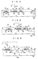
- Figs. 7 and 8 show a fourth embodiment of a semiconductor device according to the present invention.
- Fig. 7 illustrates a circuit diagram of a self substrate bias generator.
- the AC voltage generating circuit 210 grounded at one end produces an AC voltage oscillating between the reference voltage V ss and the power source voltage V DD .
- the other end of the generating circuit 210 is connected to a terminal 216 via a capacitor 212 and an N channel MOS transistor 214.
- the terminal 216 is connected to a semiconductor region to which the voltage generated by the self substrate bias generator is to be supplied.
- a node between the generating circuit 210 and the capacitor 212 is denoted as N21 and a node between the source of the transistor 214 and the capacitor 212 is denoted as N22.
- the node N22 is connected to the gate and the drain of the N channel MOS transistor grounded at the source.
- the gate of the N channel MOS transistor 214 is connected to the drain pe se.
- the substrate region in which the channel of the transistor214 is formed and the substrate region in which the channel of the transistor 218 is formed are connected together.
- N channel MOS transistors 214 and 218 are formed in a P type semiconductor region 250. Formed between the semiconductor region 250 and the node N22 is a PN junction (diode) 252 indicated by a broken line in Fig. 7.
- the MOS transistors 214 and 218 have a rectifying characteristic.
- the semiconductor region 250 where the transistors 214 and 218 are formed is separated from the semiconductor region driven by the self substrate bias generator.
- Fig. 8 shows a cross sectional view of a semiconductor device with a self substrate bias generator shown in Fig. 7 according to the present invention.
- P type well regions 222 and 250 are separately formed on the surface region of an N type silicon substrate 220.
- a major circuit made up of an N channel transistor is formed in the P type well region 222.
- N type high concentration impurity regions 224, 226, 228, 270 and 272 are formed in the surface region of the P type well region 250.
- a gate electrode 232 is formed on the P well region 250 located between the N type regions 224 and 226 with a gate insulating film 230 interposed therebetween.
- the N type region 224, gate electrode 232 and N type region 226 are the drain, the gate and the source of the N channel MOS transistor 214 in Fig.
- a gate electrode 236 is formed on the N type high concentration impurity region 228, with the gate insulating film 234 interposed therebetween.
- a capacitor 212 is formed by the gate electrode 236, the gate insulating film 234 and the N type high concentration impurity region 228.
- a gate electrode 276 is formed through a gate insulating film 274 on the P well region 250 between the N type impurity regions 270 and 272. The N type impurity region 270, the gate electrode 276 and the N type impurity region 272 serve as the drain, gate and source of the N channel MOS transistor 218, respectively.
- a P type high concentration impurity region 238 for enhancing the ohmic contact and other circuit elements are formed in the other P type well region 222.
- the gate electrode 232 of the MOS transistor 214 is connected to the N type impurity region 224 and the P type impurity region 238.
- the gate electrode 236 of the capacitor 212 is connected to ground by way of the AC voltage generating circuit 210.
- the gate electrode 276 of the MOS transistor 218 and the N type impurity region 270 of the same are connected to the N type impurity region 226 of the MOS transistor 214.
- the N type high concentration impurity layer 272 of the MOS transistor 218 is grounded.
- the power source voltage V oo is supplied to the N type semiconductor substrate 220.
- An N type high concentration impurity region 254 to ensure a complete separation between the P well regions 222 and 250 is formed in the surface region of the N type semiconductor substrate 220 sandwiched by the P well regions 222 and 250.
- the N type impurity region 254 is biased to the power source voltage V DD .
- the impurity region 254 may be formed by an insulating region such as SiO z .
- the impurity region 254 is not necessarily provided since the N type silicon substrate 220 is biased to the power source voltage V DD . However, the provision of the impurity region 254 is preferable for effectively implementing the present invention.
- An AC voltage at the electrode 236 (node N21) of the capacitor 212 oscillates between the power source voltage V DD and the reference voltage V ss by the AC voltage generating circuit 210.
- the N type impurity regions 226 and 228 (node N22) electrically oscillate due to electrostatic induction.
- the impurity regions 226, 228 and 270 are at high potential, those regions are discharged through the transistor 218.
- those regions are at low potential, those are charged through the transistor 214.
- the impurity regions 226, 228 and 270 and the P well region 250 are forwardly biased, so that electrons are injected into the P well region 250 from the regions 226, 228 and 270. Since the P type well region 250 is in a floating state, it is negatively charged by the injected electrons for a short time. Accordingly, a less amount of the injected electrons is allowed.
- the silicon substrate 220 is positively biased, even if the injected electrons in the P well region 250 enter the silicon substrate 220, the electrons never enter the negatively biased P well region 222. Further, when the N type impurity region 254 biased to the power source voltage V DD is formed, the electrons diffused toward the P well region 222 from the P well region 250 through the surface region of the N type silicon substrate can be caught. In this case, its effect is much greater. Therefore, the minority carriers generated by the self substrate bias generator do not adversely effect the operation of the circuit elements.
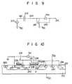
- FIG. 9 shows a circuit diagram of a self substrate bias generator.
- Fig. 10 is a cross sectional view of a semiconductor device with the self substrate bias generator shown in Fig. 9, which is according to the present invention.
- the present embodiment employs a diode 256 for the rectifier element.
- the diode 256 is a PN junction formed by a P well region 250, and N type high concentration impurity regions 226 and 228.
- N type high concentration impurity regions 226, 228, 270 and 272 Formed in the P well region 250 formed in the N type silicon substrate 220 are the N type high concentration impurity regions 226, 228, 270 and 272, and P type high concentration impurity regions 258 and 260 surrounding those impurity regions 226, 228, 270 and 272.
- the N type impurity region 228 serves as one of the electrodes of the capacitor 212.
- the P type impurity region 258 is connected to the P well region formed in the substrate 220.
- the N type impurity region 226, 228 and 270 are at low potential by the AC voltage generating circuit 210, electrons flow from the impurity regions 226, 228 and 270 into the P well region 250. It is preferable that the electrons in P type region are removed fast. To this end, the region in which the electrons recombine fast, that is, the P type high concentration impurity regions 258 and 260, are preferably formed close to and around the impurity regions 226, 228 and 270. In order to drive the recombination of electrons, it is advisable to diffuse impurity to provide the recombination center such as gold (Au) into the P well region 250.
- impurity such as gold (Au) into the P well region 250.
- the P well regions 222 and 250 are formed into the N type silicon substrate 220.
- a P type epitaxial layer may be formed on the N type silicon substrate.
- the conductivity type of the well regions and circuit elements may be set to the opposite to that of those in Figs. 8 and 9, and the polarity of the voltage applied may be inversed.
Landscapes
- Engineering & Computer Science (AREA)
- Physics & Mathematics (AREA)
- Microelectronics & Electronic Packaging (AREA)
- Nonlinear Science (AREA)
- Electromagnetism (AREA)
- General Physics & Mathematics (AREA)
- Radar, Positioning & Navigation (AREA)
- Automation & Control Theory (AREA)
- Semiconductor Integrated Circuits (AREA)
- Metal-Oxide And Bipolar Metal-Oxide Semiconductor Integrated Circuits (AREA)
Claims (11)
Applications Claiming Priority (4)
| Application Number | Priority Date | Filing Date | Title |
|---|---|---|---|
| JP56052032A JPS57166066A (en) | 1981-04-07 | 1981-04-07 | Bias generating system for substrate |
| JP52032/81 | 1981-04-07 | ||
| JP56052033A JPS57166067A (en) | 1981-04-07 | 1981-04-07 | Bias generating unit for substrate |
| JP52033/81 | 1981-04-07 |
Publications (3)
| Publication Number | Publication Date |
|---|---|
| EP0062894A2 EP0062894A2 (de) | 1982-10-20 |
| EP0062894A3 EP0062894A3 (en) | 1985-05-22 |
| EP0062894B1 true EP0062894B1 (de) | 1987-08-05 |
Family
ID=26392639
Family Applications (1)
| Application Number | Title | Priority Date | Filing Date |
|---|---|---|---|
| EP82102994A Expired EP0062894B1 (de) | 1981-04-07 | 1982-04-07 | Halbleiteranordnung |
Country Status (3)
| Country | Link |
|---|---|
| US (1) | US4559548A (de) |
| EP (1) | EP0062894B1 (de) |
| DE (1) | DE3276920D1 (de) |
Families Citing this family (36)
| Publication number | Priority date | Publication date | Assignee | Title |
|---|---|---|---|---|
| DE3743930A1 (de) * | 1987-12-23 | 1989-07-06 | Siemens Ag | Integrierte schaltung mit "latch-up"-schutzschaltung in komplementaerer mos-schaltungstechnik |
| JPS58122766A (ja) * | 1982-01-14 | 1983-07-21 | Toshiba Corp | 半導体装置 |
| US4581546A (en) * | 1983-11-02 | 1986-04-08 | Inmos Corporation | CMOS substrate bias generator having only P channel transistors in the charge pump |
| US4670669A (en) * | 1984-08-13 | 1987-06-02 | International Business Machines Corporation | Charge pumping structure for a substrate bias generator |
| US4647956A (en) * | 1985-02-12 | 1987-03-03 | Cypress Semiconductor Corp. | Back biased CMOS device with means for eliminating latchup |
| US4628214A (en) * | 1985-05-22 | 1986-12-09 | Sgs Semiconductor Corporation | Back bias generator |
| JPS6266656A (ja) * | 1985-09-19 | 1987-03-26 | Toshiba Corp | 基板電位生成回路 |
| JPH0750552B2 (ja) * | 1985-12-20 | 1995-05-31 | 三菱電機株式会社 | 内部電位発生回路 |
| JPS62155547A (ja) * | 1985-12-27 | 1987-07-10 | Mitsubishi Electric Corp | 基板電位発生装置 |
| FR2596931B1 (fr) * | 1986-04-04 | 1993-03-26 | Thomson Csf | Multiplicateur de tension continue pouvant etre integre a une structure semi-conductrice |
| US4875151A (en) * | 1986-08-11 | 1989-10-17 | Ncr Corporation | Two transistor full wave rectifier |
| US4720467A (en) * | 1986-09-29 | 1988-01-19 | International Business Machines Corporation | Method of forming a capacitor-transistor integrated circuit |
| IT1217104B (it) * | 1987-03-03 | 1990-03-14 | Sgs Microelettronica Spa | Circuito integrato cmos a due alimentazioni con un transistore mos integrato di protezione contro il <<latch-up>>. |
| US4933573A (en) * | 1987-09-18 | 1990-06-12 | Fuji Electric Co., Ltd. | Semiconductor integrated circuit |
| NL8702734A (nl) * | 1987-11-17 | 1989-06-16 | Philips Nv | Spanningsvermenigvuldigschakeling en gelijkrichtelement. |
| US5006974A (en) * | 1987-12-24 | 1991-04-09 | Waferscale Integration Inc. | On-chip high voltage generator and regulator in an integrated circuit |
| JPH0666443B2 (ja) * | 1988-07-07 | 1994-08-24 | 株式会社東芝 | 半導体メモリセルおよび半導体メモリ |
| US5008799A (en) * | 1990-04-05 | 1991-04-16 | Montalvo Antonio J | Back-to-back capacitor charge pumps |
| WO1991016728A1 (fr) * | 1990-04-13 | 1991-10-31 | Kabushiki Kaisha Toshiba | Structure de substrat pour un dispositif a semiconducteurs |
| KR930008876B1 (ko) * | 1990-08-17 | 1993-09-16 | 현대전자산업 주식회사 | 반도체소자의 고전압 발생회로 |
| US5081371A (en) * | 1990-11-07 | 1992-01-14 | U.S. Philips Corp. | Integrated charge pump circuit with back bias voltage reduction |
| JP2968836B2 (ja) * | 1990-11-30 | 1999-11-02 | 日本テキサス・インスツルメンツ株式会社 | 半導体基板電位発生回路 |
| US5364801A (en) * | 1990-12-17 | 1994-11-15 | Texas Instruments Incorporated | Method of forming a charge pump circuit |
| KR940003153B1 (ko) * | 1991-04-12 | 1994-04-15 | 금성일렉트론 주식회사 | 백바이어스 발생회로 |
| EP0582125B1 (de) * | 1992-08-04 | 1998-01-28 | Siemens Aktiengesellschaft | Ansteuerschaltung für einen Leistungs-MOSFET mit sourceseitiger Last |
| JPH0810760B2 (ja) * | 1993-01-13 | 1996-01-31 | 日本電気株式会社 | 固体撮像装置 |
| TW283239B (en) * | 1995-11-13 | 1996-08-11 | Advanced Micro Devices Inc | Improved charge pumps using accumulation capacitors |
| JPH09162713A (ja) * | 1995-12-11 | 1997-06-20 | Mitsubishi Electric Corp | 半導体集積回路 |
| US5801934A (en) * | 1996-12-12 | 1998-09-01 | Cypress Semiconductor Corp. | Charge pump with reduced power consumption |
| KR100243295B1 (ko) * | 1997-06-26 | 2000-02-01 | 윤종용 | 반도체장치의 백 바이어스 발생기 및 그 발생방법 |
| US5999425A (en) * | 1998-01-15 | 1999-12-07 | Cypress Semiconductor Corp. | Charge pump architecture for integrated circuit |
| US6075400A (en) * | 1998-08-13 | 2000-06-13 | Pericom Semiconductor Corp. | Cancellation of injected charge in a bus switch |
| US6026003A (en) * | 1998-12-18 | 2000-02-15 | Motorola, Inc. | Charge pump circuit and method for generating a bias voltage |
| US7679427B2 (en) * | 2007-06-14 | 2010-03-16 | Suvolta, Inc. | Semiconductor device including a bias voltage generator |
| US7889523B2 (en) * | 2007-10-10 | 2011-02-15 | Freescale Semiconductor, Inc. | Variable load, variable output charge-based voltage multipliers |
| US9583479B1 (en) * | 2016-01-14 | 2017-02-28 | Globalfoundries Inc. | Semiconductor charge pump with imbedded capacitor |
Family Cites Families (5)
| Publication number | Priority date | Publication date | Assignee | Title |
|---|---|---|---|---|
| NL7212509A (de) * | 1972-09-15 | 1974-03-19 | ||
| JPS5472691A (en) * | 1977-11-21 | 1979-06-11 | Toshiba Corp | Semiconductor device |
| JPS583105B2 (ja) * | 1978-02-10 | 1983-01-19 | 唐津 真一 | 金属製屋根板 |
| JPS5950224B2 (ja) * | 1978-10-30 | 1984-12-07 | 富士通株式会社 | 半導体装置 |
| JPS55107255A (en) * | 1979-02-12 | 1980-08-16 | Mitsubishi Electric Corp | Substrate potential generating circuit device |
-
1982
- 1982-04-02 US US06/364,639 patent/US4559548A/en not_active Expired - Lifetime
- 1982-04-07 DE DE8282102994T patent/DE3276920D1/de not_active Expired
- 1982-04-07 EP EP82102994A patent/EP0062894B1/de not_active Expired
Also Published As
| Publication number | Publication date |
|---|---|
| EP0062894A2 (de) | 1982-10-20 |
| EP0062894A3 (en) | 1985-05-22 |
| DE3276920D1 (en) | 1987-09-10 |
| US4559548A (en) | 1985-12-17 |
Similar Documents
| Publication | Publication Date | Title |
|---|---|---|
| EP0062894B1 (de) | Halbleiteranordnung | |
| US4591738A (en) | Charge pumping circuit | |
| US4670669A (en) | Charge pumping structure for a substrate bias generator | |
| US4377756A (en) | Substrate bias circuit | |
| KR930022373A (ko) | 챠지펌핑효율이 개선된 챠지펌프회로 | |
| EP0049273A4 (de) | Komplementärer feldeffekttransistor mit integrierter schaltung. | |
| JPH0689574A (ja) | 半導体装置 | |
| US4476479A (en) | Semiconductor device with operating voltage coupling region | |
| JPS6050066B2 (ja) | Mos半導体集積回路装置 | |
| US4356502A (en) | Protection circuit for a semiconductor device | |
| CN112838856B (zh) | 使用光伏源极的晶体管的反向本体偏置 | |
| US5497011A (en) | Semiconductor memory device and a method of using the same | |
| JP3379050B2 (ja) | 半導体装置 | |
| JPH0738434B2 (ja) | 相補性回路技術による集積回路 | |
| KR0149226B1 (ko) | 반도체 회로를 위한 정전기 보호장치 | |
| JP2978346B2 (ja) | 半導体集積回路装置の入力回路 | |
| KR930009810B1 (ko) | 기판바이어스회로를 구비한 반도체장치 | |
| JPH0219979B2 (de) | ||
| US6781804B1 (en) | Protection of the logic well of a component including an integrated MOS power transistor | |
| US4952998A (en) | Integrated circuit with complementary MOS transistors | |
| KR100618448B1 (ko) | 보호 회로를 갖는 반도체 장치 | |
| JPS62160750A (ja) | 基板電圧発生回路 | |
| KR100342591B1 (ko) | 반도체 소자 | |
| JP3127254B2 (ja) | Soi型半導体装置 | |
| JPS62154663A (ja) | 電圧発生回路 |
Legal Events
| Date | Code | Title | Description |
|---|---|---|---|
| PUAI | Public reference made under article 153(3) epc to a published international application that has entered the european phase |
Free format text: ORIGINAL CODE: 0009012 |
|
| AK | Designated contracting states |
Designated state(s): DE FR GB NL |
|
| 17P | Request for examination filed |
Effective date: 19821016 |
|
| RAP1 | Party data changed (applicant data changed or rights of an application transferred) |
Owner name: KABUSHIKI KAISHA TOSHIBA |
|
| PUAL | Search report despatched |
Free format text: ORIGINAL CODE: 0009013 |
|
| AK | Designated contracting states |
Designated state(s): DE FR GB NL |
|
| 17Q | First examination report despatched |
Effective date: 19861202 |
|
| GRAA | (expected) grant |
Free format text: ORIGINAL CODE: 0009210 |
|
| AK | Designated contracting states |
Kind code of ref document: B1 Designated state(s): DE FR GB NL |
|
| REF | Corresponds to: |
Ref document number: 3276920 Country of ref document: DE Date of ref document: 19870910 |
|
| ET | Fr: translation filed | ||
| PLBE | No opposition filed within time limit |
Free format text: ORIGINAL CODE: 0009261 |
|
| STAA | Information on the status of an ep patent application or granted ep patent |
Free format text: STATUS: NO OPPOSITION FILED WITHIN TIME LIMIT |
|
| 26N | No opposition filed | ||
| REG | Reference to a national code |
Ref country code: GB Ref legal event code: 746 Effective date: 19981130 |
|
| REG | Reference to a national code |
Ref country code: FR Ref legal event code: D6 |
|
| PGFP | Annual fee paid to national office [announced via postgrant information from national office to epo] |
Ref country code: DE Payment date: 20010402 Year of fee payment: 20 |
|
| PGFP | Annual fee paid to national office [announced via postgrant information from national office to epo] |
Ref country code: GB Payment date: 20010404 Year of fee payment: 20 |
|
| PGFP | Annual fee paid to national office [announced via postgrant information from national office to epo] |
Ref country code: FR Payment date: 20010409 Year of fee payment: 20 |
|
| PGFP | Annual fee paid to national office [announced via postgrant information from national office to epo] |
Ref country code: NL Payment date: 20010430 Year of fee payment: 20 |
|
| REG | Reference to a national code |
Ref country code: GB Ref legal event code: IF02 |
|
| PG25 | Lapsed in a contracting state [announced via postgrant information from national office to epo] |
Ref country code: GB Free format text: LAPSE BECAUSE OF EXPIRATION OF PROTECTION Effective date: 20020406 |
|
| PG25 | Lapsed in a contracting state [announced via postgrant information from national office to epo] |
Ref country code: NL Free format text: LAPSE BECAUSE OF EXPIRATION OF PROTECTION Effective date: 20020407 |
|
| REG | Reference to a national code |
Ref country code: GB Ref legal event code: PE20 Effective date: 20020406 |
|
| NLV7 | Nl: ceased due to reaching the maximum lifetime of a patent |
Effective date: 20020407 |
|
| NLV7 | Nl: ceased due to reaching the maximum lifetime of a patent |
Effective date: 20020407 |