EP0062982B1 - Integrierte Schaltung mit einer Isolationszone und mit einer Substratelektrode - Google Patents
Integrierte Schaltung mit einer Isolationszone und mit einer Substratelektrode Download PDFInfo
- Publication number
- EP0062982B1 EP0062982B1 EP82301512A EP82301512A EP0062982B1 EP 0062982 B1 EP0062982 B1 EP 0062982B1 EP 82301512 A EP82301512 A EP 82301512A EP 82301512 A EP82301512 A EP 82301512A EP 0062982 B1 EP0062982 B1 EP 0062982B1
- Authority
- EP
- European Patent Office
- Prior art keywords
- pit
- type
- semiconductor layer
- depth
- layer
- Prior art date
- Legal status (The legal status is an assumption and is not a legal conclusion. Google has not performed a legal analysis and makes no representation as to the accuracy of the status listed.)
- Expired
Links
Images


Classifications
-
- H—ELECTRICITY
- H10—SEMICONDUCTOR DEVICES; ELECTRIC SOLID-STATE DEVICES NOT OTHERWISE PROVIDED FOR
- H10W—GENERIC PACKAGES, INTERCONNECTIONS, CONNECTORS OR OTHER CONSTRUCTIONAL DETAILS OF DEVICES COVERED BY CLASS H10
- H10W10/00—Isolation regions in semiconductor bodies between components of integrated devices
- H10W10/01—Manufacture or treatment
- H10W10/011—Manufacture or treatment of isolation regions comprising dielectric materials
- H10W10/014—Manufacture or treatment of isolation regions comprising dielectric materials using trench refilling with dielectric materials, e.g. shallow trench isolations
- H10W10/0143—Manufacture or treatment of isolation regions comprising dielectric materials using trench refilling with dielectric materials, e.g. shallow trench isolations comprising concurrently refilling multiple trenches having different shapes or dimensions
-
- H—ELECTRICITY
- H10—SEMICONDUCTOR DEVICES; ELECTRIC SOLID-STATE DEVICES NOT OTHERWISE PROVIDED FOR
- H10W—GENERIC PACKAGES, INTERCONNECTIONS, CONNECTORS OR OTHER CONSTRUCTIONAL DETAILS OF DEVICES COVERED BY CLASS H10
- H10W10/00—Isolation regions in semiconductor bodies between components of integrated devices
- H10W10/01—Manufacture or treatment
- H10W10/011—Manufacture or treatment of isolation regions comprising dielectric materials
- H10W10/014—Manufacture or treatment of isolation regions comprising dielectric materials using trench refilling with dielectric materials, e.g. shallow trench isolations
- H10W10/0145—Manufacture or treatment of isolation regions comprising dielectric materials using trench refilling with dielectric materials, e.g. shallow trench isolations of trenches having shapes other than rectangular or V-shape
-
- H—ELECTRICITY
- H10—SEMICONDUCTOR DEVICES; ELECTRIC SOLID-STATE DEVICES NOT OTHERWISE PROVIDED FOR
- H10W—GENERIC PACKAGES, INTERCONNECTIONS, CONNECTORS OR OTHER CONSTRUCTIONAL DETAILS OF DEVICES COVERED BY CLASS H10
- H10W10/00—Isolation regions in semiconductor bodies between components of integrated devices
- H10W10/10—Isolation regions comprising dielectric materials
- H10W10/17—Isolation regions comprising dielectric materials formed using trench refilling with dielectric materials, e.g. shallow trench isolations
-
- H—ELECTRICITY
- H10—SEMICONDUCTOR DEVICES; ELECTRIC SOLID-STATE DEVICES NOT OTHERWISE PROVIDED FOR
- H10W—GENERIC PACKAGES, INTERCONNECTIONS, CONNECTORS OR OTHER CONSTRUCTIONAL DETAILS OF DEVICES COVERED BY CLASS H10
- H10W20/00—Interconnections in chips, wafers or substrates
- H10W20/01—Manufacture or treatment
- H10W20/021—Manufacture or treatment of interconnections within wafers or substrates
-
- Y—GENERAL TAGGING OF NEW TECHNOLOGICAL DEVELOPMENTS; GENERAL TAGGING OF CROSS-SECTIONAL TECHNOLOGIES SPANNING OVER SEVERAL SECTIONS OF THE IPC; TECHNICAL SUBJECTS COVERED BY FORMER USPC CROSS-REFERENCE ART COLLECTIONS [XRACs] AND DIGESTS
- Y10—TECHNICAL SUBJECTS COVERED BY FORMER USPC
- Y10S—TECHNICAL SUBJECTS COVERED BY FORMER USPC CROSS-REFERENCE ART COLLECTIONS [XRACs] AND DIGESTS
- Y10S148/00—Metal treatment
- Y10S148/02—Contacts, special
-
- Y—GENERAL TAGGING OF NEW TECHNOLOGICAL DEVELOPMENTS; GENERAL TAGGING OF CROSS-SECTIONAL TECHNOLOGIES SPANNING OVER SEVERAL SECTIONS OF THE IPC; TECHNICAL SUBJECTS COVERED BY FORMER USPC CROSS-REFERENCE ART COLLECTIONS [XRACs] AND DIGESTS
- Y10—TECHNICAL SUBJECTS COVERED BY FORMER USPC
- Y10S—TECHNICAL SUBJECTS COVERED BY FORMER USPC CROSS-REFERENCE ART COLLECTIONS [XRACs] AND DIGESTS
- Y10S148/00—Metal treatment
- Y10S148/124—Polycrystalline emitter
Definitions
- the present invention relates to semiconductor devices.
- a semiconductor device by means of the passive isolation method, hereinafter referred to as the PI method, there may be a requirement to provide an electrode which is electrically connected to the substrate of the semiconductor device.
- Such an electrode is hereinafter referred to as a substrate electrode.
- Fig. 1A illustrates a bipolar IC in which the PN junction isolation method is employed
- Fig. 1B illustrates a bipolar IC in which the conventional PI method is employed
- Figs. 2A, 2B, and 2C illustrate schematically known semiconductor devices in which isolation is carried out by means of the PI method, and the method of formation of a substrate electrode is improved over the electrode shown in Fig. lB
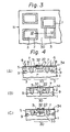
- Fig. 3 shows a partial plan view of a semiconductor device in which the PI method according to an embodiment of the present invention is employed
- Fig. 4A, 4B, and 4C are partial cross-sectional views of a semiconductor device in which the PI method according to other embodiments of the present invention is employed
- FIG. 5 illustrates a step in the production of the semiconductor device shown in Fig. 4C; and Figs. 6A and 6B illustrate cross-sectional views of a semiconductor device in the process of being produced according to embodiments of the present invention in which the anisotropic wet etching method and dry etching method are respectively employed.
- the isolation method used in the case of bipolar ICs is either the PN junction isolation method illustrated in Fig. 1A or the PI method illustrated in Fig. 1B.
- the latter method of isolation is superior to the former method of isolation because the elements of the bipolar ICs can be formed at a high integration density.
- an N type epitaxial layer 2 having a thickness of approximately 3 micrometers is formed on the P type silicon semiconductor substrate 1.
- the elements of the bipolar ICs, the transistor elements for example, are then formed on the N type epitaxial layer 2. Only one region in which one of the transistors is formed is shown in Fig. 3 and is denoted by the numeral 3. This region is hereinafter simply referred to as the element-forming region 3.
- a P + type isolation region 4 is formed in the N type epitaxial layer 2 by means of thermal diffusion of the P type impurities. Since the P type impurities diffuse laterally into an N type epitaxial layer by a larger dimension than the dimension required in the PI method, dimension tolerance L 1 , L 2 such that the P + type isolation region 4 is in contact with neither the P type base region 5 nor the N + type collector contact region 6 must be provided before thermal diffusion is performed, and therefore the integration density is disadvantageously low. Contrary to this, a high integration density can be achieved in the bipolar IC illustrate in Fig.
- the isolation region 7 comprises a silicon dioxide film or consists of an insulating material.
- the element-forming region 3 in Fig. 1B is smaller than that in Fig. 1A, and the N type epitaxial layer 2 can be used effectively for forming the elements of the bipolar ICs. Nevertheless, the formation of the substrate electrode by means of the PI method involves a problem. Referring again to Fig.
- the formation of the substrate electrode can be simply achieved by depositing the electrode material on the surface of the P + type isolation region 4.
- such region 4 can be used not only as a PN junction isolation region bust also as a means of electrically connecting the P type electrode material and the silicon semiconductor substrate 1.
- the isolation region 7 cannot be used as means of electrically connecting the electrode material and the silicon semiconductor substrate because said isolation region 7 is insulative.
- the reference numerals 8 and 9 in Figs. 1A and 1B indicative the emitter region and the N + type buried layer, respectively.
- an IC chip 11, in which the bipolar ICs are fabricated, is mounted on a package 10 made of ceramics or the like.
- the IC chip 11 is thermally bonded to a thin gold layer 12 which is formed by placing a gold pellet (not shown) on the bottom of the recess of the package 10 and then frictionally rubing the chip over the gold pellet, which is, in turn, flattened and applied to said bottom.
- the thin gold layer 12 makes possible the easy formation of the substrate electrode.
- a terminal chip 13 made of metal or silicon is thermally bonded to the thin gold layer 12 and then a wire 15 is strung between the terminal chip 13 and the lead terminal 14, with the result that a path of current or an electric lead is formed between the lead terminal 14 and the silicon semiconductor substrate (not shown) via the bottom surface of the IC chip 11.
- This process does not involve a complicated bonding operation.
- the construction of and production process of an electronic device are complicated since the terminal chip 13 is indispensable, that is, a path of current cannot be formed by means of the IC chip 11 itself.
- the dimension of the IC chip 11 is accordingly so large that no space is left for positioning the terminal chip 13.
- a thin gold layer 12 can be deposited on the package 10 beforehand, which however, is expensive. Furthermore, the thin gold layer 12 may extend from the bottom of the recess of the package 10 to the top, but this is also expensive.
- the substrate electrode is formed on the top surface of the IC chip.
- the isolation method carried out in the device shown in Fig. 2B is a method of isolation by means of oxide and poly-silicon, is referred to as the IOP (Isolation by Oxide and Poly-Silicon) method.
- IOP Isolation by Oxide and Poly-Silicon
- a V groove (V-ATE) 20 is formed by subjecting the (100) surface of the silicon semiconductor substrate 1 to anisotropic etching.
- the impurities having the same conductivity type as that of the silicon semiconductor substrate, i.e. P type in Fig. 2b, are shallowly introduced into the V-ATE 20 from the surface of the V-ATE 20, thereby forming a P type diffusion layer 21.
- Insulating material such as polycrystalline silicon
- the formation of the substrate electrode can be achieved by depositing aluminum 22 on the surface of the N type epitaxial layer 2 in such a manner that the aluminum 22 is in ohmic contact with the P type diffusion layer 21.
- the V-ATE 20 in which the insulating material is embedded, protrudes into and through the N type epitaxial layer 2 and forms an isolation region. In other words, isolation of the element-forming region 3 from the other element-forming regions is complete even if the P type diffusion layer 21 is not formed around the V-ATE 20.
- a PN junction isolation regions is formed between the N type epitaxial layer 2 and the P type diffusion layer 21, and the advantages of the PI method are lost. Therefore, such dimension tolerance as is necessary in the case of the PN junction isolation method is also necessary in the case of the IOP method.
- An advantage of the PI method basically resides in the self-alignment of the base and/or emitter regions, which advantage is, however, lost in the case of the formation of the P type diffusion layer 21.
- a P + type diffusion layer 23 which is so deep that it penetrates through the N type epitaxial layer 2 into the P type silicon semiconductor substrate 1, is formed in such a manner that it surrounds the element-forming region 3 and the isolation region 7.
- the P + type diffusion layer 23 is used to form the substrate electrode because when such a layer is used there is no decrease in the integration density since the P + type diffusion layer 23 is formed in a vacant space, i.e. in the part of the N type epitaxial layer 2 which is located between the neighbouring isolation regions (one of which is shown as "7").
- Part of the vacant space in which the P + type diffusion layer 23 is formed is not part of the element-forming region 3.
- a heat treatment at approximately 1000°C is needed.
- Such a heat treatment results in upward diffusion of the N type impurities of the N + type buried layer 9.
- the effective thickness of the N type epitaxial layer 2 is decreased during the heat treatment to such an extent that the diffusion of P type impurities in the formation of the P type base region 5 at a later stage is likely to result in contact or near contact between the N + type buried layer 9 and the P type base region 5.
- the breakdown voltage of the device is decreased.
- An embodiment of the present invention can serve to avoid, in the case of the PI method, upward diffusion of the impurities of a buried layer, and maintain one of the advantages of the PI method, i.e. self alignment, whilst forming a substrate electrode on the top surface of an IC chip.
- a method for producing a semiconductor device wherein there is formed on a semiconductor substrate, of one conductivity type, a relatively thin semiconductor layer of the opposite conductivity type, and electronic circuit elements surrounded respectively by passive isolation regions are produced in the said semiconductor layer, said method being characterized in that a pit is formed in the said semiconductor layer to a depth of at least one-quarter of the depth of said semiconductor layer, externally of each of the said passive isolation regions, and is filled with semiconductor material containing dopant appropriate to the said one conductivity type, heat treatment is applied to bring about diffusion of the said dopant from the said pit so as to produce an ohmic electrical connection between the said semiconductor material and the said substrate, and an electrode is provided on the semiconductor material in the pit.
- the said pit may be formed as a groove.
- a partial plan view of a semiconductor device which may be an IC chip or LSI chip, is shown.
- the description hereinafter refers to an IC chip.
- the passive isolation regions which are hereinafter referred to as the isolation regions, are denoted in Fig. 3 by the reference numeral 7.
- the entire surface of the IC chip 11 is not used for the element-forming regions 3, and therefore a vacant space 30 remains between the isolation regions 7.
- the substrate electrode or electrodes are formed, according to the present invention, in the semiconductor layer (not shown in Fig. 3), which is formed on the semiconductor substrate (not shown in Fig. 3) and which coincides with the vacant space 30.
- FIGs. 4A through C cross sectional views of a semiconductor device, i.e. the IC chip 11, are shown.
- the semiconductor substrate having one conductivity type is the P-type silicon semiconductor substrate 1
- the semiconductor layer having another conductivity type is the N-type epitaxial layer 2.
- the members denoted by the reference numerals 8 and 9 are the same as those in Fig. 1B.
- a groove 31 is formed in the N-type epitaxial layer 2 at the vacant space 30 by means of etching.
- a semiconductor material 32 polycrystalline silicon for example, in which the P-type impurities, e.g.
- the etching carried out so as to form the groove 31 may or may not be anisotropic etching of the (100) surface of the N-type epitaxial layer 2 or may be wet etching or dry etching, such as plasma etching.
- the groove 31 shown in Fig. 4A has a depth of from one third to one fourth the thickness of the N-type epitaxial layer 2.
- the electrode material, aluminum 22 for example, is deposited on the surface of the polycrystalline silicon layer 32.
- a heat treatment is also carried out so as to create ohmic contact between the polycrystalline silicon layer 32 and the P-type silicon semiconductor substrate 1.
- the depth of the groove 31 is half or more than half of the thickness of the N-type epitaxial layer 2 and greater than that in the case of Fig. 4A.
- the heat treatment mentioned above can be carried out atthe same time as the formation of the P-type base region 5 (not shown in Fig. 4B but shown in Fig. 4A). In other words, when thermal diffusion is carried out so as to form the P-type base region 5, ohmic contact between the polycrystalline silicon layer 32 and the P-type silicon semiconductor substrate 1 can simultaneously be realized.
- the groove 31 may penetrate to the P-type silicon semiconductor substrate 1.
- the heat treatment mentioned above is also necessary in order to create the ohmic contact mentioned above.
- the depth of the groove 31 should be at least one fourth, preferably one half and more preferably the thickness of the N-type epitaxial layer 2 from the viewpoint of lessening the diffusion of the impurities from the N +- type buried layer 9 for example. When, however, the groove 31 is deep, the width or diameter of the groove 31 is accordingly great.
- the depth of the groove 31 may be equal to or greater than the thickness of the N-type epitaxial layer 2.
- the depth of the groove 31 should be determined so that the vacant space 30 can be effectively used to achieve a high integration density and so that the diffusion length of the impurities can be made lessened as much as possible.
- the diffusion length of the impurities diffused from the semiconductor material within said at least one groove is lessened.
- a buried layer having said one conductivity type is formed and said at least one groove is formed above said buried layer. More specifically, referring to Fig. 4C, a P +- type buried layer 33 is formed and then the heat treatment is carried out so that ohmic contact between the polycrystalline silicon layer 32 and the P-type silicon semiconductor substrate 1 is created.
- the P-type impurities from the P +- type buried layer 33 are upwardly diffused and the P-type .impurities from the polycrystalline silicon layer 32 are downwardly diffused so as to form the ohmic contact mentioned above, and the P-type impurities of the P + -type buried layer 33 have a high diffusion coefficient.
- the method for forming an N + -type buried layer 9 and a P + -type buried layer 33 is apparent from the device in Fig. 5.
- the surface of the P-type silicon semiconductor substrate 1 is cleaned and a silicon dioxide film 34 is then formed on the surface.
- a window 35 is selectively formed through the silicon dioxide film 34 and the N-type impurities are thermally diffused through the window 35 so as to form the N + -type buried layer 9; then the window 35 is closed with a silicon dioxide film (not shown).
- a window 36 is then selectively formed through the silicon dioxide film 34, and the P-type impurities are thermally diffused through the window 36 so as to form the P +- type buried layer 33.
- the N +- type buried layer 9 and the P +- type buried layer 33 can also be formed by means of the ion implantation method as explained below.
- the windows 35 and 36 are selectively formed through the silicon dioxide film 34 and a photoresist film (not shown) is applied to the silicon dioxide film 34 so as to cover the windows 35 and 36.
- the photoresist film is subjected to exposure and developing, thereby exposing the P-type silicon semiconductor substrate 1 through the window 35.
- Ion implantation of N-type impurities is then carried out so that the impurities are selectively implanted in the P-type silicon semiconductor substrate 1 through the window 35.
- the application, exposure, and then development of another photoresist is applied to the silicon dioxide film 34 so as to form the windown 36, through which the P-type impurities are implanted.
- the N +- type buried layer 9 and the P +- type buried layer 33 can also be formed by means of an ion beam method in which the parts of the P-type silicon semiconductor substrate 1 exposed through the windows 35 and 36, respectively, are irradiated with N-type and P-type impurities, respectively.
- the ion beam method is easier to apply than is the ion implantation method in that selective irradiation of the P-type silicon semiconductor substrate 1 with different types impurity is possible.
- the N-type epitaxial layer (not shown in Fig. 5) is formed on the P-type silicon semiconductor substrate 1 by means of a well-known epitaxial growth method.
- the groove 31 is formed by means of conventional etching, i.e. isotropic etching, which does not have a preferential etching rate of a specific crystal plane of the semiconductor material. Therefore, the groove 31 usually has a U-shape.
- Figure 6A illustrates an embodiment of the present invention in which the at least one groove is formed by means of anisotropic wet etching of the (100) plane of the semiconductor substrate.
- An advantage of this embodiment is that said at least one groove and grooves for forming the isolation regions can be simultaneously formed.
- Another advantage is that since the relative etching rate in the vertical direction, as compared with that in the lateral direction, is high in the case of anisotropic etching, a deep groove can be formed while at the same time keeping the width of the groove small and the diffusion length of the impurites diffused from the semiconductor material filled in the groove very short. As a result, a high integration density can be achieved.
- the reference numeral 40 indicates two grooves for forming the isolation region 7 (passive isolation region) while the reference numeral 31 indicates one groove for forming the substrate electrode.
- These grooves 31 and 40 have a depth D or d which is 0.7 times the width W or w of the grooves according to preferential etching of (111) plane of a single silicon crystal.
- the depth of the groove 31 is determined the light of the diffusion length and the dimension of the vacant space as described with reference to Figs. 4A and 4B.
- the depth of the grooves 41 is determined so that the grooves 40 penetrate through the N-type epitaxial layer 2, which usually has a thickness in the range of from 3 to 4 microns.
- the depth of the grooves 31. and 40 may be different, these grooves 31 and 40 can be easily formed simultaneously simply by adjusting the width of the grooves, i.e.
- the heat treatment is carried out so as to form ohmic contact between the polycrystalline silicon layer 32 and the P-type silicon semiconductor substrate 1 and the deposition of an electrode material on the polycrystalline silicon layer 32 are carried as described hereinabove.
- the surface of the polycrystalline silicon layer 32 should be flattened so as to prevent the aluminum conductors (not shown) formed on the N-type epitaxial layer 2 from being uneven.
- Fig. 6B illustrates an embodiment of the present invention in which at least one groove (40') is formed by means of dry etching, such as plasma etching.
Landscapes
- Element Separation (AREA)
- Bipolar Transistors (AREA)
- Electrodes Of Semiconductors (AREA)
- Semiconductor Integrated Circuits (AREA)
Claims (11)
Applications Claiming Priority (2)
| Application Number | Priority Date | Filing Date | Title |
|---|---|---|---|
| JP42058/81 | 1981-03-23 | ||
| JP56042058A JPS57167653A (en) | 1981-03-23 | 1981-03-23 | Manufacture of semiconductor device |
Publications (3)
| Publication Number | Publication Date |
|---|---|
| EP0062982A2 EP0062982A2 (de) | 1982-10-20 |
| EP0062982A3 EP0062982A3 (en) | 1986-05-21 |
| EP0062982B1 true EP0062982B1 (de) | 1989-09-06 |
Family
ID=12625495
Family Applications (1)
| Application Number | Title | Priority Date | Filing Date |
|---|---|---|---|
| EP82301512A Expired EP0062982B1 (de) | 1981-03-23 | 1982-03-23 | Integrierte Schaltung mit einer Isolationszone und mit einer Substratelektrode |
Country Status (5)
| Country | Link |
|---|---|
| US (1) | US4468856A (de) |
| EP (1) | EP0062982B1 (de) |
| JP (1) | JPS57167653A (de) |
| DE (1) | DE3279934D1 (de) |
| IE (1) | IE55071B1 (de) |
Families Citing this family (3)
| Publication number | Priority date | Publication date | Assignee | Title |
|---|---|---|---|---|
| JPH061775B2 (ja) * | 1985-07-17 | 1994-01-05 | 日本電気株式会社 | 半導体装置の製造方法 |
| US5856700A (en) * | 1996-05-08 | 1999-01-05 | Harris Corporation | Semiconductor device with doped semiconductor and dielectric trench sidewall layers |
| US20150123240A1 (en) * | 2013-11-07 | 2015-05-07 | Addison R. Crockett | Semiconductor Device and Method of Forming Shallow P-N Junction with Sealed Trench Termination |
Family Cites Families (8)
| Publication number | Priority date | Publication date | Assignee | Title |
|---|---|---|---|---|
| US3752715A (en) * | 1971-11-15 | 1973-08-14 | Ibm | Production of high speed complementary transistors |
| JPS5135828B2 (de) * | 1972-07-04 | 1976-10-05 | ||
| JPS5616548B2 (de) * | 1973-08-06 | 1981-04-16 | ||
| JPS5091287A (de) * | 1973-12-12 | 1975-07-21 | ||
| JPS53115173A (en) * | 1977-03-18 | 1978-10-07 | Hitachi Ltd | Production of semiconductor device |
| US4168997A (en) * | 1978-10-10 | 1979-09-25 | National Semiconductor Corporation | Method for making integrated circuit transistors with isolation and substrate connected collectors utilizing simultaneous outdiffusion to convert an epitaxial layer |
| US4256514A (en) * | 1978-11-03 | 1981-03-17 | International Business Machines Corporation | Method for forming a narrow dimensioned region on a body |
| GB2056767A (en) * | 1979-08-16 | 1981-03-18 | Texas Instruments Inc | A process and structure for Schottky transistor logic circuit |
-
1981
- 1981-03-23 JP JP56042058A patent/JPS57167653A/ja active Pending
-
1982
- 1982-03-22 US US06/360,660 patent/US4468856A/en not_active Expired - Fee Related
- 1982-03-23 EP EP82301512A patent/EP0062982B1/de not_active Expired
- 1982-03-23 DE DE8282301512T patent/DE3279934D1/de not_active Expired
- 1982-03-23 IE IE679/82A patent/IE55071B1/en not_active IP Right Cessation
Also Published As
| Publication number | Publication date |
|---|---|
| IE55071B1 (en) | 1990-05-23 |
| EP0062982A2 (de) | 1982-10-20 |
| US4468856A (en) | 1984-09-04 |
| IE820679L (en) | 1982-09-23 |
| EP0062982A3 (en) | 1986-05-21 |
| DE3279934D1 (en) | 1989-10-12 |
| JPS57167653A (en) | 1982-10-15 |
Similar Documents
| Publication | Publication Date | Title |
|---|---|---|
| US4160991A (en) | High performance bipolar device and method for making same | |
| JP2893053B2 (ja) | 集積化された電子装置における電荷キャリアの寿命の局所化される短縮のための処理、および電荷キャリアの寿命の局所化される短縮を伴う集積化された電子装置 | |
| US4433468A (en) | Method for making semiconductor device having improved thermal stress characteristics | |
| US4161417A (en) | Method of making CMOS structure with retarded electric field for minimum latch-up | |
| CA1063731A (en) | Method for making transistor structures having impurity regions separated by a short lateral distance | |
| US3909306A (en) | MIS type semiconductor device having high operating voltage and manufacturing method | |
| JPH0754825B2 (ja) | 部分的誘電体分離半導体装置 | |
| US4236294A (en) | High performance bipolar device and method for making same | |
| US4910572A (en) | Semiconductor device and method of fabricating the same | |
| JP2002110978A (ja) | 電力用半導体素子 | |
| EP0091686B1 (de) | Halbleiteranordnung mit diffundierter Zone mit reduzierter Länge und Verfahren zur Herstellung dieser Zone | |
| US4845051A (en) | Buried gate JFET | |
| NL8701251A (nl) | Halfgeleiderinrichting en werkwijze ter vervaardiging daarvan. | |
| JP2002016080A (ja) | トレンチゲート型mosfetの製造方法 | |
| US4498224A (en) | Method of manufacturing a MOSFET using accelerated ions to form an amorphous region | |
| KR100272051B1 (ko) | 접점윈도우를통해베이스주입한p-채널mos게이트소자제조공정 | |
| EP0062982B1 (de) | Integrierte Schaltung mit einer Isolationszone und mit einer Substratelektrode | |
| KR100762523B1 (ko) | 개량된 반도체 트렌치 모스 디바이스를 제조하는 방법 | |
| US5264381A (en) | Method of manufacturing a static induction type switching device | |
| JP3247106B2 (ja) | 集積回路の製法と集積回路構造 | |
| JP2687489B2 (ja) | 半導体装置 | |
| KR100206193B1 (ko) | 전력반도체장치 및 그의 제조방법 | |
| JP2948892B2 (ja) | Mos電界効果トランジスタおよびその製造方法 | |
| KR100268866B1 (ko) | 반도체 소자 및 이의 제조방법 | |
| KR0173964B1 (ko) | 래치업 제어구조를 갖는 전력반도체장치의 제조방법 |
Legal Events
| Date | Code | Title | Description |
|---|---|---|---|
| PUAI | Public reference made under article 153(3) epc to a published international application that has entered the european phase |
Free format text: ORIGINAL CODE: 0009012 |
|
| AK | Designated contracting states |
Designated state(s): DE FR GB NL |
|
| PUAL | Search report despatched |
Free format text: ORIGINAL CODE: 0009013 |
|
| AK | Designated contracting states |
Kind code of ref document: A3 Designated state(s): DE FR GB NL |
|
| 17P | Request for examination filed |
Effective date: 19861112 |
|
| 17Q | First examination report despatched |
Effective date: 19880318 |
|
| GRAA | (expected) grant |
Free format text: ORIGINAL CODE: 0009210 |
|
| AK | Designated contracting states |
Kind code of ref document: B1 Designated state(s): DE FR GB |
|
| REF | Corresponds to: |
Ref document number: 3279934 Country of ref document: DE Date of ref document: 19891012 |
|
| ET | Fr: translation filed | ||
| PLBE | No opposition filed within time limit |
Free format text: ORIGINAL CODE: 0009261 |
|
| STAA | Information on the status of an ep patent application or granted ep patent |
Free format text: STATUS: NO OPPOSITION FILED WITHIN TIME LIMIT |
|
| 26N | No opposition filed | ||
| PGFP | Annual fee paid to national office [announced via postgrant information from national office to epo] |
Ref country code: FR Payment date: 19950309 Year of fee payment: 14 |
|
| PGFP | Annual fee paid to national office [announced via postgrant information from national office to epo] |
Ref country code: GB Payment date: 19950315 Year of fee payment: 14 |
|
| PGFP | Annual fee paid to national office [announced via postgrant information from national office to epo] |
Ref country code: DE Payment date: 19950322 Year of fee payment: 14 |
|
| PG25 | Lapsed in a contracting state [announced via postgrant information from national office to epo] |
Ref country code: GB Effective date: 19960323 |
|
| GBPC | Gb: european patent ceased through non-payment of renewal fee |
Effective date: 19960323 |
|
| PG25 | Lapsed in a contracting state [announced via postgrant information from national office to epo] |
Ref country code: FR Effective date: 19961129 |
|
| PG25 | Lapsed in a contracting state [announced via postgrant information from national office to epo] |
Ref country code: DE Effective date: 19961203 |
|
| REG | Reference to a national code |
Ref country code: FR Ref legal event code: ST |