EP0062982A2 - Integrierte Schaltung mit einer Isolationszone und mit einer Substratelektrode - Google Patents
Integrierte Schaltung mit einer Isolationszone und mit einer Substratelektrode Download PDFInfo
- Publication number
- EP0062982A2 EP0062982A2 EP82301512A EP82301512A EP0062982A2 EP 0062982 A2 EP0062982 A2 EP 0062982A2 EP 82301512 A EP82301512 A EP 82301512A EP 82301512 A EP82301512 A EP 82301512A EP 0062982 A2 EP0062982 A2 EP 0062982A2
- Authority
- EP
- European Patent Office
- Prior art keywords
- pit
- semiconductor layer
- type
- semiconductor
- substrate
- Prior art date
- Legal status (The legal status is an assumption and is not a legal conclusion. Google has not performed a legal analysis and makes no representation as to the accuracy of the status listed.)
- Granted
Links
Images


Classifications
-
- H—ELECTRICITY
- H10—SEMICONDUCTOR DEVICES; ELECTRIC SOLID-STATE DEVICES NOT OTHERWISE PROVIDED FOR
- H10W—GENERIC PACKAGES, INTERCONNECTIONS, CONNECTORS OR OTHER CONSTRUCTIONAL DETAILS OF DEVICES COVERED BY CLASS H10
- H10W10/00—Isolation regions in semiconductor bodies between components of integrated devices
- H10W10/01—Manufacture or treatment
- H10W10/011—Manufacture or treatment of isolation regions comprising dielectric materials
- H10W10/014—Manufacture or treatment of isolation regions comprising dielectric materials using trench refilling with dielectric materials, e.g. shallow trench isolations
- H10W10/0143—Manufacture or treatment of isolation regions comprising dielectric materials using trench refilling with dielectric materials, e.g. shallow trench isolations comprising concurrently refilling multiple trenches having different shapes or dimensions
-
- H—ELECTRICITY
- H10—SEMICONDUCTOR DEVICES; ELECTRIC SOLID-STATE DEVICES NOT OTHERWISE PROVIDED FOR
- H10W—GENERIC PACKAGES, INTERCONNECTIONS, CONNECTORS OR OTHER CONSTRUCTIONAL DETAILS OF DEVICES COVERED BY CLASS H10
- H10W10/00—Isolation regions in semiconductor bodies between components of integrated devices
- H10W10/01—Manufacture or treatment
- H10W10/011—Manufacture or treatment of isolation regions comprising dielectric materials
- H10W10/014—Manufacture or treatment of isolation regions comprising dielectric materials using trench refilling with dielectric materials, e.g. shallow trench isolations
- H10W10/0145—Manufacture or treatment of isolation regions comprising dielectric materials using trench refilling with dielectric materials, e.g. shallow trench isolations of trenches having shapes other than rectangular or V-shape
-
- H—ELECTRICITY
- H10—SEMICONDUCTOR DEVICES; ELECTRIC SOLID-STATE DEVICES NOT OTHERWISE PROVIDED FOR
- H10W—GENERIC PACKAGES, INTERCONNECTIONS, CONNECTORS OR OTHER CONSTRUCTIONAL DETAILS OF DEVICES COVERED BY CLASS H10
- H10W10/00—Isolation regions in semiconductor bodies between components of integrated devices
- H10W10/10—Isolation regions comprising dielectric materials
- H10W10/17—Isolation regions comprising dielectric materials formed using trench refilling with dielectric materials, e.g. shallow trench isolations
-
- H—ELECTRICITY
- H10—SEMICONDUCTOR DEVICES; ELECTRIC SOLID-STATE DEVICES NOT OTHERWISE PROVIDED FOR
- H10W—GENERIC PACKAGES, INTERCONNECTIONS, CONNECTORS OR OTHER CONSTRUCTIONAL DETAILS OF DEVICES COVERED BY CLASS H10
- H10W20/00—Interconnections in chips, wafers or substrates
- H10W20/01—Manufacture or treatment
- H10W20/021—Manufacture or treatment of interconnections within wafers or substrates
-
- Y—GENERAL TAGGING OF NEW TECHNOLOGICAL DEVELOPMENTS; GENERAL TAGGING OF CROSS-SECTIONAL TECHNOLOGIES SPANNING OVER SEVERAL SECTIONS OF THE IPC; TECHNICAL SUBJECTS COVERED BY FORMER USPC CROSS-REFERENCE ART COLLECTIONS [XRACs] AND DIGESTS
- Y10—TECHNICAL SUBJECTS COVERED BY FORMER USPC
- Y10S—TECHNICAL SUBJECTS COVERED BY FORMER USPC CROSS-REFERENCE ART COLLECTIONS [XRACs] AND DIGESTS
- Y10S148/00—Metal treatment
- Y10S148/02—Contacts, special
-
- Y—GENERAL TAGGING OF NEW TECHNOLOGICAL DEVELOPMENTS; GENERAL TAGGING OF CROSS-SECTIONAL TECHNOLOGIES SPANNING OVER SEVERAL SECTIONS OF THE IPC; TECHNICAL SUBJECTS COVERED BY FORMER USPC CROSS-REFERENCE ART COLLECTIONS [XRACs] AND DIGESTS
- Y10—TECHNICAL SUBJECTS COVERED BY FORMER USPC
- Y10S—TECHNICAL SUBJECTS COVERED BY FORMER USPC CROSS-REFERENCE ART COLLECTIONS [XRACs] AND DIGESTS
- Y10S148/00—Metal treatment
- Y10S148/124—Polycrystalline emitter
Definitions
- An embodiment of the present invention can serve to avoid, in the case of the PI method, upward diffusion of the impurities of a buried layer, and maintain one of the advantages of the PI method, i.e. self-alignment, whilst forming a substrate electrode on the top surface of an IC chip.
- a semiconductor device having:
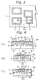
- the etching carried out so as to form the groove 31 may or may not be anisotropic etching of the (100) surface of the N-type epitaxial layer 2 or may be wet etching or dry etching, such as plasma etching.
- the groove 31 shown in Fig. 4A has a depth of from one third to one fourth the thickness of the N-type epitaxial layer 2.
- the electrode material, aluminum 22 for example, is deposited on the surface of the polycrystalline silicon layer 32.
- the depth of the groove 31 should be at least one fourth, preferably one half and more preferably the thickness of the N-type epitaxial layer 2 from the viewpoint of lessening the diffusion of the impurities from the N -type buried layer 9 for example. When, however, the groove 31 is deep, the width or diameter of the groove 31 is accordingly great.
- the depth of the groove 31 may be equal to or greater than the thickness of the N-type epitaxial layer 2.
- the depth of the groove 31 should be determined so that the vacant space 30 can be effectively used to achieve a high integration density and so that the diffusion length of the impurities can be made lessened as much as possible.
- the P-type impurities from the P +- type buried layer 33 are upwardly diffused and the P-type impurities from the polycrystalline silicon layer 32 are downwardly diffused so as to form the ohmic contact mentioned above, and the P-type impurities of the P +- type buried layer 32, antimony for example, have a high diffusion coefficient.
- the groove 31 is formed by means of conventional etching, i.e. isotropic etching, which does not have a preferential etching rate of a specific crystal plane of the semiconductor material. Therefore, the groove 31 usually has a U-shape.
- Figure 6A illustrates an embodiment of the present invention in which the at least one groove is formed by means of anisotropic wet etching of the (100) plane of the semiconductor substrate.
- An advantage of this embodiment is that said at least one groove and grooves for forming the isolation regions can be simultaneously formed.
- Another advantage is that since the relative etching rate in the vertical direction, as compared with that in the lateral direction, is high in the case of anisotropic etching, a deep groove can be formed while at the same time keeping the width of the groove small and the diffusion length of the impurities diffused from the semiconductor material filled in the groove very short. As a result, a high integration density can be achieved.
- the reference numeral 40 indicates two grooves for forming the isolation region 7 (passive isolation region) while the reference numeral 31 indicates one groove for forming the substrate electrode.
Landscapes
- Element Separation (AREA)
- Bipolar Transistors (AREA)
- Electrodes Of Semiconductors (AREA)
- Semiconductor Integrated Circuits (AREA)
Applications Claiming Priority (2)
| Application Number | Priority Date | Filing Date | Title |
|---|---|---|---|
| JP42058/81 | 1981-03-23 | ||
| JP56042058A JPS57167653A (en) | 1981-03-23 | 1981-03-23 | Manufacture of semiconductor device |
Publications (3)
| Publication Number | Publication Date |
|---|---|
| EP0062982A2 true EP0062982A2 (de) | 1982-10-20 |
| EP0062982A3 EP0062982A3 (en) | 1986-05-21 |
| EP0062982B1 EP0062982B1 (de) | 1989-09-06 |
Family
ID=12625495
Family Applications (1)
| Application Number | Title | Priority Date | Filing Date |
|---|---|---|---|
| EP82301512A Expired EP0062982B1 (de) | 1981-03-23 | 1982-03-23 | Integrierte Schaltung mit einer Isolationszone und mit einer Substratelektrode |
Country Status (5)
| Country | Link |
|---|---|
| US (1) | US4468856A (de) |
| EP (1) | EP0062982B1 (de) |
| JP (1) | JPS57167653A (de) |
| DE (1) | DE3279934D1 (de) |
| IE (1) | IE55071B1 (de) |
Families Citing this family (3)
| Publication number | Priority date | Publication date | Assignee | Title |
|---|---|---|---|---|
| JPH061775B2 (ja) * | 1985-07-17 | 1994-01-05 | 日本電気株式会社 | 半導体装置の製造方法 |
| US5856700A (en) * | 1996-05-08 | 1999-01-05 | Harris Corporation | Semiconductor device with doped semiconductor and dielectric trench sidewall layers |
| US20150123240A1 (en) * | 2013-11-07 | 2015-05-07 | Addison R. Crockett | Semiconductor Device and Method of Forming Shallow P-N Junction with Sealed Trench Termination |
Family Cites Families (8)
| Publication number | Priority date | Publication date | Assignee | Title |
|---|---|---|---|---|
| US3752715A (en) * | 1971-11-15 | 1973-08-14 | Ibm | Production of high speed complementary transistors |
| JPS5135828B2 (de) * | 1972-07-04 | 1976-10-05 | ||
| JPS5616548B2 (de) * | 1973-08-06 | 1981-04-16 | ||
| JPS5091287A (de) * | 1973-12-12 | 1975-07-21 | ||
| JPS53115173A (en) * | 1977-03-18 | 1978-10-07 | Hitachi Ltd | Production of semiconductor device |
| US4168997A (en) * | 1978-10-10 | 1979-09-25 | National Semiconductor Corporation | Method for making integrated circuit transistors with isolation and substrate connected collectors utilizing simultaneous outdiffusion to convert an epitaxial layer |
| US4256514A (en) * | 1978-11-03 | 1981-03-17 | International Business Machines Corporation | Method for forming a narrow dimensioned region on a body |
| GB2056767A (en) * | 1979-08-16 | 1981-03-18 | Texas Instruments Inc | A process and structure for Schottky transistor logic circuit |
-
1981
- 1981-03-23 JP JP56042058A patent/JPS57167653A/ja active Pending
-
1982
- 1982-03-22 US US06/360,660 patent/US4468856A/en not_active Expired - Fee Related
- 1982-03-23 EP EP82301512A patent/EP0062982B1/de not_active Expired
- 1982-03-23 DE DE8282301512T patent/DE3279934D1/de not_active Expired
- 1982-03-23 IE IE679/82A patent/IE55071B1/en not_active IP Right Cessation
Also Published As
| Publication number | Publication date |
|---|---|
| IE55071B1 (en) | 1990-05-23 |
| US4468856A (en) | 1984-09-04 |
| EP0062982B1 (de) | 1989-09-06 |
| IE820679L (en) | 1982-09-23 |
| EP0062982A3 (en) | 1986-05-21 |
| DE3279934D1 (en) | 1989-10-12 |
| JPS57167653A (en) | 1982-10-15 |
Similar Documents
| Publication | Publication Date | Title |
|---|---|---|
| JP2893053B2 (ja) | 集積化された電子装置における電荷キャリアの寿命の局所化される短縮のための処理、および電荷キャリアの寿命の局所化される短縮を伴う集積化された電子装置 | |
| JP3495257B2 (ja) | 半導体デバイスの製造方法 | |
| US7297604B2 (en) | Semiconductor device having dual isolation structure and method of fabricating the same | |
| US4160991A (en) | High performance bipolar device and method for making same | |
| JPH0754825B2 (ja) | 部分的誘電体分離半導体装置 | |
| CA1063731A (en) | Method for making transistor structures having impurity regions separated by a short lateral distance | |
| US3909306A (en) | MIS type semiconductor device having high operating voltage and manufacturing method | |
| US4236294A (en) | High performance bipolar device and method for making same | |
| JPS6080276A (ja) | 半導体素子の形成方法 | |
| US4845051A (en) | Buried gate JFET | |
| NL8701251A (nl) | Halfgeleiderinrichting en werkwijze ter vervaardiging daarvan. | |
| US5106770A (en) | Method of manufacturing semiconductor devices | |
| KR100187735B1 (ko) | 캐리어 라이프타임을 제어하는 반도체 디바이스 및 이의 제조 방법 | |
| JP2002016080A (ja) | トレンチゲート型mosfetの製造方法 | |
| US4649638A (en) | Construction of short-length electrode in semiconductor device | |
| JP2006527914A5 (de) | ||
| US6878605B2 (en) | Methods for manufacturing SOI substrate using wafer bonding and complementary high voltage bipolar transistor using the SOI substrate | |
| EP0062982B1 (de) | Integrierte Schaltung mit einer Isolationszone und mit einer Substratelektrode | |
| KR100762523B1 (ko) | 개량된 반도체 트렌치 모스 디바이스를 제조하는 방법 | |
| JPH0621365A (ja) | 半導体集積回路装置及びその製造方法 | |
| JP2687489B2 (ja) | 半導体装置 | |
| KR100268866B1 (ko) | 반도체 소자 및 이의 제조방법 | |
| JP3447592B2 (ja) | 半導体装置とその製造方法 | |
| KR100481984B1 (ko) | 반도체장치및그제조방법 | |
| KR0173964B1 (ko) | 래치업 제어구조를 갖는 전력반도체장치의 제조방법 |
Legal Events
| Date | Code | Title | Description |
|---|---|---|---|
| PUAI | Public reference made under article 153(3) epc to a published international application that has entered the european phase |
Free format text: ORIGINAL CODE: 0009012 |
|
| AK | Designated contracting states |
Designated state(s): DE FR GB NL |
|
| PUAL | Search report despatched |
Free format text: ORIGINAL CODE: 0009013 |
|
| AK | Designated contracting states |
Kind code of ref document: A3 Designated state(s): DE FR GB NL |
|
| 17P | Request for examination filed |
Effective date: 19861112 |
|
| 17Q | First examination report despatched |
Effective date: 19880318 |
|
| GRAA | (expected) grant |
Free format text: ORIGINAL CODE: 0009210 |
|
| AK | Designated contracting states |
Kind code of ref document: B1 Designated state(s): DE FR GB |
|
| REF | Corresponds to: |
Ref document number: 3279934 Country of ref document: DE Date of ref document: 19891012 |
|
| ET | Fr: translation filed | ||
| PLBE | No opposition filed within time limit |
Free format text: ORIGINAL CODE: 0009261 |
|
| STAA | Information on the status of an ep patent application or granted ep patent |
Free format text: STATUS: NO OPPOSITION FILED WITHIN TIME LIMIT |
|
| 26N | No opposition filed | ||
| PGFP | Annual fee paid to national office [announced via postgrant information from national office to epo] |
Ref country code: FR Payment date: 19950309 Year of fee payment: 14 |
|
| PGFP | Annual fee paid to national office [announced via postgrant information from national office to epo] |
Ref country code: GB Payment date: 19950315 Year of fee payment: 14 |
|
| PGFP | Annual fee paid to national office [announced via postgrant information from national office to epo] |
Ref country code: DE Payment date: 19950322 Year of fee payment: 14 |
|
| PG25 | Lapsed in a contracting state [announced via postgrant information from national office to epo] |
Ref country code: GB Effective date: 19960323 |
|
| GBPC | Gb: european patent ceased through non-payment of renewal fee |
Effective date: 19960323 |
|
| PG25 | Lapsed in a contracting state [announced via postgrant information from national office to epo] |
Ref country code: FR Effective date: 19961129 |
|
| PG25 | Lapsed in a contracting state [announced via postgrant information from national office to epo] |
Ref country code: DE Effective date: 19961203 |
|
| REG | Reference to a national code |
Ref country code: FR Ref legal event code: ST |