EP0063455A1 - Procédé de fabrication de dispositifs de groupes microélectroniques scellés, chimiquement sensibles - Google Patents
Procédé de fabrication de dispositifs de groupes microélectroniques scellés, chimiquement sensibles Download PDFInfo
- Publication number
- EP0063455A1 EP0063455A1 EP19820301867 EP82301867A EP0063455A1 EP 0063455 A1 EP0063455 A1 EP 0063455A1 EP 19820301867 EP19820301867 EP 19820301867 EP 82301867 A EP82301867 A EP 82301867A EP 0063455 A1 EP0063455 A1 EP 0063455A1
- Authority
- EP
- European Patent Office
- Prior art keywords
- ion
- transducer
- channel
- semiconductor
- mode
- Prior art date
- Legal status (The legal status is an assumption and is not a legal conclusion. Google has not performed a legal analysis and makes no representation as to the accuracy of the status listed.)
- Granted
Links
Images


Classifications
-
- H—ELECTRICITY
- H10—SEMICONDUCTOR DEVICES; ELECTRIC SOLID-STATE DEVICES NOT OTHERWISE PROVIDED FOR
- H10D—INORGANIC ELECTRIC SEMICONDUCTOR DEVICES
- H10D64/00—Electrodes of devices having potential barriers
- H10D64/60—Electrodes characterised by their materials
- H10D64/66—Electrodes having a conductor capacitively coupled to a semiconductor by an insulator, e.g. MIS electrodes
- H10D64/68—Electrodes having a conductor capacitively coupled to a semiconductor by an insulator, e.g. MIS electrodes characterised by the insulator, e.g. by the gate insulator
- H10D64/681—Electrodes having a conductor capacitively coupled to a semiconductor by an insulator, e.g. MIS electrodes characterised by the insulator, e.g. by the gate insulator having a compositional variation, e.g. multilayered
- H10D64/685—Electrodes having a conductor capacitively coupled to a semiconductor by an insulator, e.g. MIS electrodes characterised by the insulator, e.g. by the gate insulator having a compositional variation, e.g. multilayered being perpendicular to the channel plane
-
- A—HUMAN NECESSITIES
- A61—MEDICAL OR VETERINARY SCIENCE; HYGIENE
- A61B—DIAGNOSIS; SURGERY; IDENTIFICATION
- A61B5/00—Measuring for diagnostic purposes; Identification of persons
- A61B5/145—Measuring characteristics of blood in vivo, e.g. gas concentration or pH-value ; Measuring characteristics of body fluids or tissues, e.g. interstitial fluid or cerebral tissue
- A61B5/14542—Measuring characteristics of blood in vivo, e.g. gas concentration or pH-value ; Measuring characteristics of body fluids or tissues, e.g. interstitial fluid or cerebral tissue for measuring blood gases
-
- A—HUMAN NECESSITIES
- A61—MEDICAL OR VETERINARY SCIENCE; HYGIENE
- A61B—DIAGNOSIS; SURGERY; IDENTIFICATION
- A61B5/00—Measuring for diagnostic purposes; Identification of persons
- A61B5/145—Measuring characteristics of blood in vivo, e.g. gas concentration or pH-value ; Measuring characteristics of body fluids or tissues, e.g. interstitial fluid or cerebral tissue
- A61B5/1468—Measuring characteristics of blood in vivo, e.g. gas concentration or pH-value ; Measuring characteristics of body fluids or tissues, e.g. interstitial fluid or cerebral tissue using chemical or electrochemical methods, e.g. by polarographic means
- A61B5/1473—Measuring characteristics of blood in vivo, e.g. gas concentration or pH-value ; Measuring characteristics of body fluids or tissues, e.g. interstitial fluid or cerebral tissue using chemical or electrochemical methods, e.g. by polarographic means invasive, e.g. introduced into the body by a catheter
-
- G—PHYSICS
- G01—MEASURING; TESTING
- G01N—INVESTIGATING OR ANALYSING MATERIALS BY DETERMINING THEIR CHEMICAL OR PHYSICAL PROPERTIES
- G01N27/00—Investigating or analysing materials by the use of electric, electrochemical, or magnetic means
- G01N27/26—Investigating or analysing materials by the use of electric, electrochemical, or magnetic means by investigating electrochemical variables; by using electrolysis or electrophoresis
- G01N27/403—Cells and electrode assemblies
- G01N27/414—Ion-sensitive or chemical field-effect transistors, i.e. ISFETS or CHEMFETS
-
- G—PHYSICS
- G11—INFORMATION STORAGE
- G11C—STATIC STORES
- G11C13/00—Digital stores characterised by the use of storage elements not covered by groups G11C11/00, G11C23/00, or G11C25/00
- G11C13/02—Digital stores characterised by the use of storage elements not covered by groups G11C11/00, G11C23/00, or G11C25/00 using elements whose operation depends upon chemical change
-
- H—ELECTRICITY
- H10—SEMICONDUCTOR DEVICES; ELECTRIC SOLID-STATE DEVICES NOT OTHERWISE PROVIDED FOR
- H10D—INORGANIC ELECTRIC SEMICONDUCTOR DEVICES
- H10D64/00—Electrodes of devices having potential barriers
- H10D64/60—Electrodes characterised by their materials
- H10D64/66—Electrodes having a conductor capacitively coupled to a semiconductor by an insulator, e.g. MIS electrodes
- H10D64/68—Electrodes having a conductor capacitively coupled to a semiconductor by an insulator, e.g. MIS electrodes characterised by the insulator, e.g. by the gate insulator
- H10D64/693—Electrodes having a conductor capacitively coupled to a semiconductor by an insulator, e.g. MIS electrodes characterised by the insulator, e.g. by the gate insulator the insulator comprising nitrogen, e.g. nitrides, oxynitrides or nitrogen-doped materials
-
- H—ELECTRICITY
- H10—SEMICONDUCTOR DEVICES; ELECTRIC SOLID-STATE DEVICES NOT OTHERWISE PROVIDED FOR
- H10W—GENERIC PACKAGES, INTERCONNECTIONS, CONNECTORS OR OTHER CONSTRUCTIONAL DETAILS OF DEVICES COVERED BY CLASS H10
- H10W74/00—Encapsulations, e.g. protective coatings
- H10W74/01—Manufacture or treatment
-
- H—ELECTRICITY
- H10—SEMICONDUCTOR DEVICES; ELECTRIC SOLID-STATE DEVICES NOT OTHERWISE PROVIDED FOR
- H10W—GENERIC PACKAGES, INTERCONNECTIONS, CONNECTORS OR OTHER CONSTRUCTIONAL DETAILS OF DEVICES COVERED BY CLASS H10
- H10W74/00—Encapsulations, e.g. protective coatings
- H10W74/10—Encapsulations, e.g. protective coatings characterised by their shape or disposition
- H10W74/131—Encapsulations, e.g. protective coatings characterised by their shape or disposition the semiconductor body being only partially enclosed
- H10W74/147—Encapsulations, e.g. protective coatings characterised by their shape or disposition the semiconductor body being only partially enclosed the encapsulations being multilayered
-
- H—ELECTRICITY
- H10—SEMICONDUCTOR DEVICES; ELECTRIC SOLID-STATE DEVICES NOT OTHERWISE PROVIDED FOR
- H10W—GENERIC PACKAGES, INTERCONNECTIONS, CONNECTORS OR OTHER CONSTRUCTIONAL DETAILS OF DEVICES COVERED BY CLASS H10
- H10W74/00—Encapsulations, e.g. protective coatings
- H10W74/40—Encapsulations, e.g. protective coatings characterised by their materials
- H10W74/47—Encapsulations, e.g. protective coatings characterised by their materials comprising organic materials, e.g. plastics or resins
-
- H—ELECTRICITY
- H10—SEMICONDUCTOR DEVICES; ELECTRIC SOLID-STATE DEVICES NOT OTHERWISE PROVIDED FOR
- H10W—GENERIC PACKAGES, INTERCONNECTIONS, CONNECTORS OR OTHER CONSTRUCTIONAL DETAILS OF DEVICES COVERED BY CLASS H10
- H10W72/00—Interconnections or connectors in packages
- H10W72/50—Bond wires
- H10W72/551—Materials of bond wires
- H10W72/552—Materials of bond wires comprising metals or metalloids, e.g. silver
-
- H—ELECTRICITY
- H10—SEMICONDUCTOR DEVICES; ELECTRIC SOLID-STATE DEVICES NOT OTHERWISE PROVIDED FOR
- H10W—GENERIC PACKAGES, INTERCONNECTIONS, CONNECTORS OR OTHER CONSTRUCTIONAL DETAILS OF DEVICES COVERED BY CLASS H10
- H10W90/00—Package configurations
- H10W90/701—Package configurations characterised by the relative positions of pads or connectors relative to package parts
- H10W90/751—Package configurations characterised by the relative positions of pads or connectors relative to package parts of bond wires
- H10W90/753—Package configurations characterised by the relative positions of pads or connectors relative to package parts of bond wires between laterally-adjacent chips
-
- H—ELECTRICITY
- H10—SEMICONDUCTOR DEVICES; ELECTRIC SOLID-STATE DEVICES NOT OTHERWISE PROVIDED FOR
- H10W—GENERIC PACKAGES, INTERCONNECTIONS, CONNECTORS OR OTHER CONSTRUCTIONAL DETAILS OF DEVICES COVERED BY CLASS H10
- H10W90/00—Package configurations
- H10W90/701—Package configurations characterised by the relative positions of pads or connectors relative to package parts
- H10W90/751—Package configurations characterised by the relative positions of pads or connectors relative to package parts of bond wires
- H10W90/754—Package configurations characterised by the relative positions of pads or connectors relative to package parts of bond wires between a chip and a stacked insulating package substrate, interposer or RDL
-
- Y—GENERAL TAGGING OF NEW TECHNOLOGICAL DEVELOPMENTS; GENERAL TAGGING OF CROSS-SECTIONAL TECHNOLOGIES SPANNING OVER SEVERAL SECTIONS OF THE IPC; TECHNICAL SUBJECTS COVERED BY FORMER USPC CROSS-REFERENCE ART COLLECTIONS [XRACs] AND DIGESTS
- Y10—TECHNICAL SUBJECTS COVERED BY FORMER USPC
- Y10T—TECHNICAL SUBJECTS COVERED BY FORMER US CLASSIFICATION
- Y10T29/00—Metal working
- Y10T29/49—Method of mechanical manufacture
- Y10T29/49002—Electrical device making
Definitions
- This invention relates to field-effect transistor (FET) transducer devices.
- the invention relates particularly to encapsulated microelectronic arrays of individual, selective, chemical-sensitive FET transducers for use in the separate or simultaneous detection and/or measurement of various chemical properties.
- Chemical properties shall be understood to includecion activity and concentration, presence and concentration of enzymes, substrates, antibodies, antigens, hormones and reducible gases and the.presence, concentration and activity of any of a variety of chemical and biochemical substances including the constituents of enzymatic systems e.g. serum enzymes, glucose, lactates, pyruvates, creatinine, urea and the constituents of the immunochemical system).
- ion-selective electrodes although the large, conventional types are not well suited to clinical application due to their expense, fragility, bulk, high electrical impedance and large volume deadspace.
- a number of various types of ion-selective electrodes are known, for example glass electrodes responsive to hydrogen, sodium, potassium and other ions in solution. Ion-selective electrodes are not restricted to glass as electroactive material; other solids such as lanthanum fluoride for a fluoride-responsive electrode (Frant, M.S., U.K. Pat. 1131 574 (1968); U.S. Pat.
- ISFETs ion-sensitive field-effect transistors
- the gate insulation material (silicon dioxide, Si0 2 ) becomes hydrated after exposure to solution and functions in the fashion of a cation-responsive glass.
- hydration and ionic contamination of gate insulation material is a well-known cause of device instability and failure in the microelectronics industry where ion-barriers of silicon nitride and also ion-getters such as glasses incorporating pentavalent atoms, for example phosphorus, are used to minimize such contamination.
- the problems of gate-insulation contamination and also the gradual dissolution of SiO 2 adversely affect the quality of such devices as chemical sensors.
- a further major difficulty lies in restricting, and isolating physically, the chemically-sensitive areas on the microelectronic device and maintaining the requisite electrical characteristics.
- any electrical current flowing by the passage of charge-carriers between the electrical connections to the active device and the electrolyte in contact with the chemoresponsive areas compromises the stability of the device.
- the present state-of-the-art for device encapsulation is by crude methods such as brush encapsulation of epoxy resin under a microscope.
- the failure rate of devices fabricated by such techniques is high due to the penetration of electrolyte under the epoxy coating beyond the required boundary of the active area.
- This hand-application of insulating material is labour intensive and hence costly, and is incompatible with the highly sophisticated state-of-the-art for the mass production of electronic devices.
- the first of these aforementioned disclosures concerns the use of electroactive materials other than hydrated silicon dioxide as the chemosensitive membrane used by ISFET devices.
- the formation of such films has been carried out by hand application under a microscope in a manner similar to that of the encapsulation material and is therefore not suited to the mass-production of chemosensitive microelectronic devices.
- the second of these disclosures is concerned with devices having a similar sectional structure to those in the first disclosure, but radically different plan geometry which. confers an advantage insofar as the encapsulation technology is, to some extent, improved, but still requires a degree of manual involvement.
- two major shortcomings are thereby introduced; the process is not . readily compatible with arrays of more than two devices selective to different chemical substances, and the . extended, diffused source and drain regions, having high aspect ratios, greatly degrade the electrochemical sensitivity of the devices and introduce cross-modulation problems and furthermore greatly increase the overall temperature dependance of the output signal.
- the present invention relates to devices operating primarily in "depletion-mode” or “enhancement/depletion-mode” (Sze, S.M., Physics of Semiconductor Devices, (1969), John Wiley and Sons Inc., p. 538) where a permanent, lightly doped conducting channel between source and drain, and of the same polarity, is provided by diffusion, use of an epitaxially grown film, ion-implantation or other means; such that no gate bias voltage is necessary for satisfactory operation.
- depletion-mode or “enhancement/depletion-mode”
- the present invention is concerned with the solution of the aforementioned, problems so that reliable, chemical-sensitive FET transducers can be achieved at relatively low cost by improvements in keeping with the highly developed methodology of the semiconductor industry, and provides a suitably encapsulated microelectronic array of chemosensitive FET transducers for detecting .and measuring the chemical properties of the solution phase to which the device is exposed.
- the invention provides a chemical-responsive field-effect transducer adapted to operate in depletion-mode, or enhancement/depletion-mode, comprising: a semiconductor.material having a pair of adjacent diffusion regions (1,2) of a certain doping polarity located at the surface and separated by a channel (3) of the same doping polarity, said diffusion regions and channel region being supported by an insulating substrate (4) or semiconductor substrate of opposite polarity; electrical insulator (6) and/or ion-barrier material (7) overlying the aforementioned channel region; and an electroactive material (10) overlying said insulator and/or ion barrier, such that the electroactive material can interact with substances to which it is exposed and control the charge-carrier density in the aforementioned channel.
- the transducer is fitted with a cuvette-type cap to form a flow through analytical cell for the purposes of on-line, ex-vivo biomedical application, for example, where the assembly is required to be located remotely to the associated electronic, signal-processing system, for example, strapped to a patient's arm and connected directly to a locally placed intravenous catheter for the purposes of continuous or intermittent monitoring of blood electrolyte levels.
- This mode of .operation confers both ethical and technical advantages, which are described hereinafter, over direct, in-vivo application.
- the aforementioned array, fabricated on a single semiconductor element ('chip'), comprises a plurality of discrete ISFET devices all being similar in structure with the exception of the electroactive substance or substances employed as the chemically- responsive gate film by each device.
- the following description pertains to a single device of which the aforementioned array is composed.
- the structure is shown in Fig.l in front elevation, and is characterized by two adjacent, diffused, semiconductor regions 1,2 with certain polarity created on a substrate 3 of the same polarity, such that the diffused regions are heavily doped (e .g. 10 20 cm -3 ) and permit ohmic, metallic connection, whereas the sub-- strate material is only lightly doped (e.-g. 10 17 cm -3 ) with impurities and therefore slightly electrically conducting.
- the substrate is mechanically supported by an insulator 4 as is common in state-of-the-art silicon-on-sapphire (SOS) technology, or on semiconductor material of the opposite polarity to the diffused and substrate material, such that a metallic back connection,5 may be established.
- SOS state-of-the-art silicon-on-sapphire
- this particular method of fabrication is used to create a plurality of devices on the same silicon element (Pig 2A) it is necessary to isolate individual devices with diffusions 12 deeper than, and of the opposite polarity to, the source 1, drain 2 and epitaxial layer 3, such diffusions being known as 'channel-stoppers'.
- the depletion-mode channel can be created by local diffusion (Fig 2B), for example the source 1 and drain 2 regions may be heavily doped n-type material, the channel 3 lightly doped n-type material, and the semiconductor bulk 4 lightly doped p-type.
- Fig 2B local diffusion
- the source 1 and drain 2 regions may be heavily doped n-type material, the channel 3 lightly doped n-type material, and the semiconductor bulk 4 lightly doped p-type.
- Fig 2C lightly conducting
- the surface of the device is covered by an insulating oxide film 6 which is typically thermally grown SiO 2 and may be 50 nm thick over the channel between the diffused regions and 500 nm thick over the remaining surface.
- An ion-barrier film 7 is formed-on top of the Si0 2 , for example 50 nm of pyrolitically deposited S i 3N4 . Electrical connection is made to the diffused regions by etching holes through films 6, 7 using known photolithographic techniques and evaporating a metal film, typically aluminium 400 nm thick for _connection to n-type silicon, to form contacts to the surface 8 and drain 9.
- the composite gate insulator 6, 7 is coated with an electroactive material or materials 10 using well known thick-film or thin-film techniques; for example, doped polymer ion-selective membranes may be selectively deposited using a thick-film screening process; ion-selective glasses may be deposited through a photoresist mask using the relief photomask technique to define the areas of deposition.
- the device, or array of devices is affixed to a header, which may be a CERDIP, TO-5 metal pack or other suitable mount known to the microelectronics industry, and wire-bonding used to form electrical interconnections.
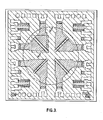
- a suitable encapsulating agent 11 in such a way that only the chemosensitive areas of the devices remain exposed; this process is detailed hereinafter and is facilitated by choosing an appropriate layout geometry for the device array, such as that shown in Fig 3 which represents a plan diagram of the 3.9 mm square NCL 03 chip. Heavily stippled areas represent heavily doped n-type regions (n + ); lightly stipped areas represent semiconductor bulk material (p ); black areas represent contact holes through gate dielectric and ion-barrier films for electrical access by the metallization films, which are indicated by white areas, as will be readily appreciated and understood by those skilled in the art.
- the chip comprises four MOSFET devices and four chemosensitive devices all symmetrically orientated about an axes at.90°.
- Dotted circle B represents the encapsulant boundary, such that it surrounds.the chemoresponsive areas of the four devices which must remain exposed while the rest of the chip is sealed during encapsulation.
- the square A represents the chemoresponsive area ('gate') of the device in the upper-left quadrant.
- Fig 4 shows a quadrant of the chip in greater detail, where dotted rectangle 13 represents a lightly doped channel region (3 in Fig 2B); 5 is the bonding pad for connection to the semiconductor bulk; 14, 15 and 16 are the MOSFET bonding pads connected to source, gate and drain respectively.
- the bulk and source connections of the chemoresponsive devices may be joined to form a common leadout in order to reduce the number of electrical connections required, or the array may be designed to have a common source region, with a plurality of associated channels and drains.
- An important aspect of the present invention is the encapsulating agent.and means by which encapsulation is effected.
- Encapsulation is achieved by the use of materials such as Bis-GMA, and adduct of bis-phenol A and glycidyl methacrylate [2,2-bis (p-(2-hydroxy 3-methacryloxy propoxy) phenyl) propane], or Bis-GMA urethane adduct, which are polymerized by U.V. irradiation or other appropriate means, and restricted physically in the area of their application by an appropriate directed jet of air or inert gas.
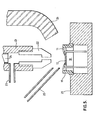
- the microelectronic device array 17 is mounted onto a transistor or integrated-circuit header 18, as hereinbefore described with appropriate wire-bonded interconnections.
- a ring-type collar 19 is affixed to the header 18 and around the device 17.
- This assembly is temporarily mounted on a jig 20, being capable of movement in the horizontal plane using an x - y positioning drive, which is used to-align the horizontally disposed semiconductor device surface underneath a jet of gas directed downwards onto, and orthogonally with respect to, the latter.
- the gas jet is supplied by a fixture 21 having a gas inlet port 23, a venturi 22 and a visible or near visible light source which may be a fibre-optic terminator 24.
- Encapsulant material 11 is added to the inner edge of the restraining collar 19 with a hypodermic needle 25, whereupon the materials flows completely around the collar and perimeter of the device such as to envelope the metal wire-bonding and bonding pads, but the material is prohibited from flowing onto the centre of the device 17 by the radial, outward gas flow from the incident gas jet.
- the encapsulation material 11 is then rapidly polymerized by irradiation with U.V. light which may be appropriately directed through a U.V.
- optical aids may be used to assist in the alignment of the gas jet with the chemoresponsive areas.
- Light from the fibre-optic source 24 is collimated by-the gas-jet venturi 22 and provides a small illuminated area on the chip surface 17 which is, by necessity, accurately aligned with the central axis of the gas jet.
- the symmetrical structure of the device hereinbefore described (Fig 3) is such that the optically induced drain currents flowing in the individual devices may be simultaneously processed electronically and the resulting information used to drive the aforementioned x-y-positioner, and hence jig 20, thus optimally servo- controlling the position of the device with respect to the gas jet and allowing fully automatic encapsulation. This is a significant improvement on prior-art.
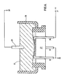
- Fig 6 The method of application of encapsulated chemosensitive semiconductor device arrays is shown in Fig 6, where the encapsulated device 27 comprises a header 18, device 17, collar 19 and encapsulating agent 11 as shown in Fig 5.
- the device 17 is that described by Figs 1 to 4.
- Lead out wires from the device source 32 and semiconductor bulk 33 are connected to ground 30.
- Drain connection 34 is connected to a low voltage source 31 (typically 2 to 5V) and the device is exposed to the electrolyte sample under analysis 35, shown in this instance in an open cuvette 28.
- the electrolyte sample is grounded with a conventional reference electrode 29 which may be a calomel, porous- junction unit. No polarising voltage is necessary between reference electrode 29,.and ground 30, as is required by previous disclosures concerned with enhancement-mode sensors.
- the electrical potential in the bulk of the chemoresponsive film 10 (Fig. 1), with respect to the electrolyte, is determined by electrochemical reactions occuring at the film/electrolyte interface and is dependant upon the chemical properties of the latter.
- This potential referred to.the semiconductor bulk 4 via the reference electrode 29, controls the electrical charge density in the channel between source 1 and drain 2 regions, and hence the electrical current flowing between source and drain under the influence of the external voltage source 31.
- the device effectively transforms a signal related to chemical properties directly into a low impedance current source.
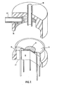
- Fig 7 shows an encapsulated device 27 as hereinbefore described, together with a flow-through cap 36 having fluid inlet 38 and fluid outlet 37 ports.
- a low pressure applied to 37 (with respect to 38) sucks fluid directly onto the sensor surface and provides an efficient flow-through assembly with small volume deadspace which is ideally suited for connection to an intravenous catheter for the purpose of continuous or intermittent ex-vivo, on-line blood analysis in conjunction with local, inexpensive signal processing/ control hardware.
- This mode of operation is superior to in-vivo application for the following reasons.
- the physical nature of the encapsulated device 27 is also ideal for the mass production of single- function solid-state ion-selective electrodes, as the shape of the encapsulation material provides a former into which doped polymer films may be readily cast, using well-known materials and methodology, as will be appreciated by those skilled in the art.
Landscapes
- Health & Medical Sciences (AREA)
- Life Sciences & Earth Sciences (AREA)
- Physics & Mathematics (AREA)
- Molecular Biology (AREA)
- Chemical & Material Sciences (AREA)
- General Health & Medical Sciences (AREA)
- Pathology (AREA)
- Engineering & Computer Science (AREA)
- Animal Behavior & Ethology (AREA)
- Optics & Photonics (AREA)
- Heart & Thoracic Surgery (AREA)
- Surgery (AREA)
- Biomedical Technology (AREA)
- Biophysics (AREA)
- Public Health (AREA)
- Veterinary Medicine (AREA)
- Chemical Kinetics & Catalysis (AREA)
- Medical Informatics (AREA)
- Microelectronics & Electronic Packaging (AREA)
- Electrochemistry (AREA)
- Analytical Chemistry (AREA)
- Biochemistry (AREA)
- General Physics & Mathematics (AREA)
- Immunology (AREA)
- General Chemical & Material Sciences (AREA)
- Investigating Or Analyzing Materials By The Use Of Electric Means (AREA)
Applications Claiming Priority (2)
| Application Number | Priority Date | Filing Date | Title |
|---|---|---|---|
| GB8111199 | 1981-04-09 | ||
| GB8111199A GB2096825A (en) | 1981-04-09 | 1981-04-09 | Chemical sensitive semiconductor field effect transducer |
Related Child Applications (1)
| Application Number | Title | Priority Date | Filing Date |
|---|---|---|---|
| EP86200343.1 Division-Into | 1986-03-06 |
Publications (2)
| Publication Number | Publication Date |
|---|---|
| EP0063455A1 true EP0063455A1 (fr) | 1982-10-27 |
| EP0063455B1 EP0063455B1 (fr) | 1987-07-08 |
Family
ID=10521051
Family Applications (2)
| Application Number | Title | Priority Date | Filing Date |
|---|---|---|---|
| EP19860200343 Expired - Lifetime EP0193251B1 (fr) | 1981-04-09 | 1982-04-08 | Dispositif de groupes microélectroniques enrobés, chimiquement sensibles |
| EP19820301867 Expired EP0063455B1 (fr) | 1981-04-09 | 1982-04-08 | Procédé de fabrication de dispositifs de groupes microélectroniques scellés, chimiquement sensibles |
Family Applications Before (1)
| Application Number | Title | Priority Date | Filing Date |
|---|---|---|---|
| EP19860200343 Expired - Lifetime EP0193251B1 (fr) | 1981-04-09 | 1982-04-08 | Dispositif de groupes microélectroniques enrobés, chimiquement sensibles |
Country Status (4)
| Country | Link |
|---|---|
| US (2) | US4502938A (fr) |
| EP (2) | EP0193251B1 (fr) |
| DE (2) | DE3276722D1 (fr) |
| GB (1) | GB2096825A (fr) |
Cited By (5)
| Publication number | Priority date | Publication date | Assignee | Title |
|---|---|---|---|---|
| EP0149330A1 (fr) * | 1983-12-08 | 1985-07-24 | General Signal Corporation | Capteur ISFET et procédé de fabrication |
| EP0215546A3 (fr) * | 1985-09-14 | 1989-06-21 | Thorn Emi Plc | Dispositif semi-conducteur chimiquement sensible |
| DE3816457A1 (de) * | 1988-05-13 | 1989-11-23 | Josowicz Mira | Verfahren zur verkapselung von elektronischen bauelementen |
| US5138251A (en) * | 1989-10-04 | 1992-08-11 | Olympus Optical Co., Ltd. | Fet sensor apparatus of flow-cell adaptive type and method of manufacturing the same |
| EP0643299A1 (fr) * | 1993-09-15 | 1995-03-15 | Ciba Corning Diagnostics Corp. | Matériau pour établir un contact à l'état solide pour une électrode sélective aux ions |
Families Citing this family (87)
| Publication number | Priority date | Publication date | Assignee | Title |
|---|---|---|---|---|
| US4644380A (en) * | 1977-12-08 | 1987-02-17 | University Of Pennsylvania | Substance-sensitive electrical structures |
| US5141868A (en) * | 1984-06-13 | 1992-08-25 | Internationale Octrooi Maatschappij "Octropa" Bv | Device for use in chemical test procedures |
| GB8416994D0 (en) * | 1984-07-04 | 1984-08-08 | Emi Ltd | Gas sensor |
| US4936956A (en) * | 1984-11-23 | 1990-06-26 | Massachusetts Institute Of Technology | Microelectrochemical devices based on inorganic redox active material and method for sensing |
| US4769795A (en) * | 1985-05-16 | 1988-09-06 | F. Massa | Method of making an underwater electroacoustic transducer with long-lasting high leakage resistance |
| US4911801A (en) * | 1985-10-01 | 1990-03-27 | University Of Utah | Electrically conductive polyparaphenylene polymers, and methods for their preparation and use |
| JPS62244139A (ja) * | 1986-04-17 | 1987-10-24 | Citizen Watch Co Ltd | 樹脂封止型ピングリツドアレイ及びその製造方法 |
| US4871442A (en) * | 1986-05-01 | 1989-10-03 | Terumo Corporation | Ion sensor |
| US4958295A (en) * | 1986-05-21 | 1990-09-18 | Hercules Incorporated | Analyzing apparatus and method for analysis of liquid samples |
| US4874500A (en) * | 1987-07-15 | 1989-10-17 | Sri International | Microelectrochemical sensor and sensor array |
| DE68918584T2 (de) * | 1988-03-03 | 1995-01-26 | Foxboro Co | Geschützter drucksensor. |
| US4993265A (en) * | 1988-03-03 | 1991-02-19 | The Foxboro Company | Protected pressure sensor and method of making |
| US4881885A (en) * | 1988-04-15 | 1989-11-21 | International Business Machines Corporation | Dam for lead encapsulation |
| US4961886A (en) * | 1988-06-09 | 1990-10-09 | Dow Corning Corporation | Method of controlling flow by a radiation formed dam |
| DE3827314C1 (fr) * | 1988-08-11 | 1989-10-19 | Christoff Prof. Dr. Braeuchle | |
| IT1224606B (it) * | 1988-10-10 | 1990-10-04 | Eniricerche Spa | Sensore chimico monolitico a membrana ione selettiva di tipo chemfet eprocedimento per la sua realizzazione |
| US4974592A (en) * | 1988-11-14 | 1990-12-04 | American Sensor Systems Corporation | Continuous on-line blood monitoring system |
| GB8911607D0 (en) * | 1989-05-19 | 1989-07-05 | Emi Plc Thorn | A method of encapsulation for electronic devices and devices so encapsulated |
| JPH0322543A (ja) * | 1989-06-05 | 1991-01-30 | Siemens Ag | 電子デバイスの被覆方法及び装置 |
| US5491097A (en) * | 1989-06-15 | 1996-02-13 | Biocircuits Corporation | Analyte detection with multilayered bioelectronic conductivity sensors |
| US5573649A (en) * | 1991-03-20 | 1996-11-12 | Fujitsu Limited | Miniaturized oxygen electrode and process of producing same |
| JP3152727B2 (ja) * | 1992-03-31 | 2001-04-03 | 株式会社東芝 | ノズル型分析装置 |
| US5700697A (en) * | 1993-02-01 | 1997-12-23 | Silicon Packaging Technology | Method for packaging an integrated circuit using a reconstructed package |
| US5911862A (en) * | 1993-09-15 | 1999-06-15 | Chiron Diagnostics Corporation | Material for establishing solid state contact for ion selective electrodes |
| US5591139A (en) * | 1994-06-06 | 1997-01-07 | The Regents Of The University Of California | IC-processed microneedles |
| US5902551A (en) * | 1995-01-13 | 1999-05-11 | Semi-Gas Systems, Inc. | Process gas docking station with point-of-use filter for receiving removable purifier cartridges |
| US5719033A (en) * | 1995-06-28 | 1998-02-17 | Motorola, Inc. | Thin film transistor bio/chemical sensor |
| RU2075980C1 (ru) * | 1996-01-18 | 1997-03-27 | Акционерное общество открытого типа "Завод "Компонент" | Электростимулятор желудочно-кишечного тракта |
| NL1004651C2 (nl) * | 1996-11-29 | 1998-06-03 | Nedcard | Werkwijze voor het inkapselen van een chip op een drager. |
| GB2321336B (en) * | 1997-01-15 | 2001-07-25 | Univ Warwick | Gas-sensing semiconductor devices |
| US5866442A (en) | 1997-01-28 | 1999-02-02 | Micron Technology, Inc. | Method and apparatus for filling a gap between spaced layers of a semiconductor |
| US6060327A (en) | 1997-05-14 | 2000-05-09 | Keensense, Inc. | Molecular wire injection sensors |
| US6699667B2 (en) | 1997-05-14 | 2004-03-02 | Keensense, Inc. | Molecular wire injection sensors |
| US7220550B2 (en) * | 1997-05-14 | 2007-05-22 | Keensense, Inc. | Molecular wire injection sensors |
| US6218687B1 (en) * | 1998-12-21 | 2001-04-17 | General Atomics | Smart microsensor arrays with silicon-on-insulator readouts for damage control |
| US6287451B1 (en) | 1999-06-02 | 2001-09-11 | Handani Winarta | Disposable sensor and method of making |
| TW434704B (en) * | 1999-06-11 | 2001-05-16 | Univ Nat Yunlin Sci & Tech | Device of amorphous WO3 ion sensitive field effect transistor (ISFET) and method for making the same |
| CN100347537C (zh) * | 1999-11-15 | 2007-11-07 | 松下电器产业株式会社 | 生物传感器 |
| JP2002039990A (ja) * | 2000-07-21 | 2002-02-06 | Fuji Photo Film Co Ltd | イオン選択性電極およびその製造方法 |
| US6576102B1 (en) | 2001-03-23 | 2003-06-10 | Virotek, L.L.C. | Electrochemical sensor and method thereof |
| US6572745B2 (en) * | 2001-03-23 | 2003-06-03 | Virotek, L.L.C. | Electrochemical sensor and method thereof |
| US20030055360A1 (en) * | 2001-09-05 | 2003-03-20 | Zeleznik Matthew A. | Minimally invasive sensing system for measuring rigidity of anatomical matter |
| US6997343B2 (en) | 2001-11-14 | 2006-02-14 | Hypoguard Limited | Sensor dispensing device |
| US20030111357A1 (en) * | 2001-12-13 | 2003-06-19 | Black Murdo M. | Test meter calibration |
| US6884663B2 (en) * | 2002-01-07 | 2005-04-26 | Delphon Industries, Llc | Method for reconstructing an integrated circuit package using lapping |
| US6813828B2 (en) | 2002-01-07 | 2004-11-09 | Gel Pak L.L.C. | Method for deconstructing an integrated circuit package using lapping |
| US6894359B2 (en) * | 2002-09-04 | 2005-05-17 | Nanomix, Inc. | Sensitivity control for nanotube sensors |
| US20030169426A1 (en) * | 2002-03-08 | 2003-09-11 | Peterson Timothy A. | Test member orientation |
| US6837976B2 (en) * | 2002-04-19 | 2005-01-04 | Nova Biomedical Corporation | Disposable sensor with enhanced sample port inlet |
| TW533593B (en) * | 2002-05-20 | 2003-05-21 | Univ Nat Yunlin Sci & Tech | Method of manufacturing amorphous hydrocarbon pH ion sensitive field effect transistor and method and device of measuring temperature parameter, drift and hysteresis thereof |
| US7948041B2 (en) | 2005-05-19 | 2011-05-24 | Nanomix, Inc. | Sensor having a thin-film inhibition layer |
| US7250095B2 (en) * | 2002-07-11 | 2007-07-31 | Hypoguard Limited | Enzyme electrodes and method of manufacture |
| US6852996B2 (en) * | 2002-09-25 | 2005-02-08 | Stmicroelectronics, Inc. | Organic semiconductor sensor device |
| US20040152211A1 (en) * | 2002-11-15 | 2004-08-05 | The Regents Of The University Of California | System and method for multiplexed biomolecular analysis |
| US7344678B2 (en) * | 2002-11-15 | 2008-03-18 | The Regents Of The University Of California | Composite sensor membrane |
| US7264139B2 (en) * | 2003-01-14 | 2007-09-04 | Hypoguard Limited | Sensor dispensing device |
| DE10318501A1 (de) * | 2003-04-24 | 2005-01-05 | Robert Bosch Gmbh | Chipaufbau in einem Premold-Gehäuse |
| US7383071B1 (en) | 2003-04-25 | 2008-06-03 | United States Of America As Represented By The Secretary Of The Navy | Microsensor system and method for measuring data |
| WO2005026694A2 (fr) * | 2003-09-12 | 2005-03-24 | Nanomix, Inc. | Capteur nanoelectronique de dioxyde de carbone |
| US20050121826A1 (en) * | 2003-12-03 | 2005-06-09 | Kiamars Hajizadeh | Multi-sensor device for motorized meter and methods thereof |
| US20050150763A1 (en) * | 2004-01-09 | 2005-07-14 | Butters Colin W. | Biosensor and method of manufacture |
| EP1706734A1 (fr) * | 2004-01-21 | 2006-10-04 | Rosemount Analytical Inc. | Capteur transistor a effet de champ sensible aux ions (isfet) a configuration de grille amelioree |
| US8308922B2 (en) | 2004-01-29 | 2012-11-13 | Siemens Aktiengesellschaft | Electrochemical transducer array and use thereof |
| BRPI0507376A (pt) | 2004-02-06 | 2007-07-10 | Bayer Healthcare Llc | espécie oxidável como uma referência interna para biossensores e método de uso |
| US20050255448A1 (en) * | 2004-05-13 | 2005-11-17 | Arun Majumdar | System for amplifying optical detection of cantilever deflection |
| US8536661B1 (en) | 2004-06-25 | 2013-09-17 | University Of Hawaii | Biosensor chip sensor protection methods |
| DE102004031316B3 (de) * | 2004-06-29 | 2005-12-29 | Robert Bosch Gmbh | Gassensor-Modul zur spektroskopischen Messung einer Gaskonzentration |
| US7364684B2 (en) * | 2004-08-16 | 2008-04-29 | Delphi Technologies, Inc. | Method of making an encapsulated microelectronic package having fluid carrying encapsulant channels |
| EP1916520B1 (fr) | 2004-11-26 | 2010-09-01 | Micronas GmbH | Composant électrique |
| US7777283B2 (en) | 2004-11-26 | 2010-08-17 | Micronas Gmbh | Electric component |
| JP5385607B2 (ja) | 2005-07-20 | 2014-01-08 | バイエル・ヘルスケア・エルエルシー | ゲート化電流測定器 |
| KR20130100022A (ko) | 2005-09-30 | 2013-09-06 | 바이엘 헬스케어 엘엘씨 | 게이트형 전압 전류 측정 분석물 결정 방법 |
| BRPI0717620A2 (pt) | 2006-10-24 | 2013-10-22 | Bayer Healthcare Llc | Amperometria de decaimento transitório |
| US7327303B1 (en) | 2007-03-27 | 2008-02-05 | Information Systems Laboratories, Inc. | Hybrid radar receiver |
| WO2008122390A1 (fr) * | 2007-04-05 | 2008-10-16 | Micronas Gmbh | Détecteur d'humidité et procédé de mesure de l'humidité d'un milieu gazeux |
| WO2009076302A1 (fr) | 2007-12-10 | 2009-06-18 | Bayer Healthcare Llc | Marqueurs de contrôle pour la détection automatique d'une solution de contrôle et procédés d'utilisation |
| DE102009055297A1 (de) * | 2009-12-23 | 2011-06-30 | Endress + Hauser Conducta Gesellschaft für Mess- und Regeltechnik mbH + Co. KG, 70839 | Verfahren zum Betreiben eines ISFET-Sensors |
| CZ303976B6 (cs) * | 2010-12-21 | 2013-07-24 | Masarykova Univerzita | Zarízení rozdelující tok tekutiny do více kanálu a jeho pouzití |
| CA2933321C (fr) * | 2013-09-18 | 2021-11-09 | Suprasensor Technologies, Llc | Dispositifs de transistor a effet de champ chimiques (chemfet) bases sur un recepteur moleculaire, systemes et procedes de surveillance de nitrate in situ dans des sols de champ |
| ES2542927R1 (es) * | 2014-02-11 | 2015-09-09 | Consejo Superior De Investigaciones Científicas (Csic) | Sensor de iones basado en medida diferencial, método de fabricación y método de medida |
| DE102014110560A1 (de) | 2014-07-25 | 2016-01-28 | Epcos Ag | Sensorelement, Sensoranordnung und Verfahren zur Herstellung eines Sensorelements und einer Sensoranordnung |
| DE102014110553A1 (de) | 2014-07-25 | 2016-01-28 | Epcos Ag | Sensorelement, Sensoranordnung und Verfahren zur Herstellung eines Sensorelements |
| WO2016037662A1 (fr) * | 2014-09-12 | 2016-03-17 | Siemens Aktiengesellschaft | Détecteur d'helicobacter pylori avec capteur de ph |
| WO2016037663A1 (fr) * | 2014-09-12 | 2016-03-17 | Siemens Aktiengesellschaft | Capteur de helicobacter pylori à base d'un transistor chimique à effet de champ |
| GB201608758D0 (en) | 2016-05-18 | 2016-06-29 | Dnae Group Holdings Ltd | Improvements in or relating to packaging for integrated circuits |
| KR101954250B1 (ko) * | 2016-06-03 | 2019-03-05 | 서울대학교 산학협력단 | Fet형 센서 어레이 |
| EP3853604B1 (fr) | 2018-09-21 | 2025-05-07 | Teralytic Holdings Inc. | Plate-forme de fusion de capteurs multimode extensible pour détection de sol proximale à distance |
Citations (7)
| Publication number | Priority date | Publication date | Assignee | Title |
|---|---|---|---|---|
| US3431182A (en) * | 1966-02-04 | 1969-03-04 | Orion Research | Fluoride sensitive electrode and method of using same |
| CH479870A (de) * | 1966-08-09 | 1969-10-15 | Simon Wilhelm | Ionenspezifisches Elektrodensystem |
| GB1529743A (en) * | 1975-03-12 | 1978-10-25 | Univ Utah | Selective chemical sensitive devices |
| DE2822787A1 (de) * | 1977-05-26 | 1978-12-07 | Kuraray Co | Selektiv chemisch empfindlicher fet-wandler |
| FR2400258A1 (fr) * | 1977-08-11 | 1979-03-09 | Bbc Brown Boveri & Cie | Transistor a effet de champ et a sensibilite chimique et son procede de realisation |
| GB2010011A (en) * | 1977-11-04 | 1979-06-20 | Matsuo T | Selective chemical-sensitive fet transistor device and method for the manufacture of the same |
| US4198851A (en) * | 1978-05-22 | 1980-04-22 | University Of Utah | Method and structure for detecting the concentration of oxygen in a substance |
Family Cites Families (12)
| Publication number | Priority date | Publication date | Assignee | Title |
|---|---|---|---|---|
| US788379A (en) * | 1905-01-09 | 1905-04-25 | Abraham L Rich | Method of rock-facing. |
| US2004465A (en) * | 1930-02-26 | 1935-06-11 | Walker Cement Products Inc | Cement shingle |
| GB890923A (en) * | 1959-10-20 | 1962-03-07 | British Oxygen Co Ltd | Method of and apparatus for oxygen determination |
| US3560601A (en) * | 1968-11-25 | 1971-02-02 | Ford Motor Co | Process for manufacturing porous thermoplastic sheet material |
| US3985848A (en) * | 1974-12-05 | 1976-10-12 | Bredero Price, B.V. | Method for cutting concrete coated pipe |
| US4377544A (en) * | 1974-12-10 | 1983-03-22 | Rasmussen O B | Manufacture of a textile-like reticular product from thermoplastic film |
| US4238757A (en) * | 1976-03-19 | 1980-12-09 | General Electric Company | Field effect transistor for detection of biological reactions |
| US4180771A (en) * | 1977-12-02 | 1979-12-25 | Airco, Inc. | Chemical-sensitive field-effect transistor |
| NO141682C (no) * | 1978-06-07 | 1980-05-07 | Norcem As | Fremgangsmaate til fremstilling av betonglegemer med et frilagt moenster. |
| JPS5480079A (en) * | 1978-08-07 | 1979-06-26 | Dai Ichi Seiko Co Ltd | Method of forming semiconductor seal |
| JPS5564759U (fr) * | 1978-10-27 | 1980-05-02 | ||
| JPS5626250A (en) * | 1979-08-10 | 1981-03-13 | Olympus Optical Co Ltd | Composite chemical sensor |
-
1981
- 1981-04-09 GB GB8111199A patent/GB2096825A/en not_active Withdrawn
-
1982
- 1982-04-08 US US06/366,722 patent/US4502938A/en not_active Expired - Fee Related
- 1982-04-08 EP EP19860200343 patent/EP0193251B1/fr not_active Expired - Lifetime
- 1982-04-08 DE DE8282301867T patent/DE3276722D1/de not_active Expired
- 1982-04-08 DE DE8686200343T patent/DE3280313D1/de not_active Expired - Lifetime
- 1982-04-08 EP EP19820301867 patent/EP0063455B1/fr not_active Expired
-
1984
- 1984-06-04 US US06/617,271 patent/US4567006A/en not_active Expired - Fee Related
Patent Citations (7)
| Publication number | Priority date | Publication date | Assignee | Title |
|---|---|---|---|---|
| US3431182A (en) * | 1966-02-04 | 1969-03-04 | Orion Research | Fluoride sensitive electrode and method of using same |
| CH479870A (de) * | 1966-08-09 | 1969-10-15 | Simon Wilhelm | Ionenspezifisches Elektrodensystem |
| GB1529743A (en) * | 1975-03-12 | 1978-10-25 | Univ Utah | Selective chemical sensitive devices |
| DE2822787A1 (de) * | 1977-05-26 | 1978-12-07 | Kuraray Co | Selektiv chemisch empfindlicher fet-wandler |
| FR2400258A1 (fr) * | 1977-08-11 | 1979-03-09 | Bbc Brown Boveri & Cie | Transistor a effet de champ et a sensibilite chimique et son procede de realisation |
| GB2010011A (en) * | 1977-11-04 | 1979-06-20 | Matsuo T | Selective chemical-sensitive fet transistor device and method for the manufacture of the same |
| US4198851A (en) * | 1978-05-22 | 1980-04-22 | University Of Utah | Method and structure for detecting the concentration of oxygen in a substance |
Non-Patent Citations (1)
| Title |
|---|
| IEEE TRANSACTIONS ON BIO-MEDICAL ENGINEERING, Vol. BME-17, January 1970, P. BERGVELD: "Development of an Ion-Sensitive Solid-State Device for Neurophysiological Measurements" pages 70 to 71 * |
Cited By (5)
| Publication number | Priority date | Publication date | Assignee | Title |
|---|---|---|---|---|
| EP0149330A1 (fr) * | 1983-12-08 | 1985-07-24 | General Signal Corporation | Capteur ISFET et procédé de fabrication |
| EP0215546A3 (fr) * | 1985-09-14 | 1989-06-21 | Thorn Emi Plc | Dispositif semi-conducteur chimiquement sensible |
| DE3816457A1 (de) * | 1988-05-13 | 1989-11-23 | Josowicz Mira | Verfahren zur verkapselung von elektronischen bauelementen |
| US5138251A (en) * | 1989-10-04 | 1992-08-11 | Olympus Optical Co., Ltd. | Fet sensor apparatus of flow-cell adaptive type and method of manufacturing the same |
| EP0643299A1 (fr) * | 1993-09-15 | 1995-03-15 | Ciba Corning Diagnostics Corp. | Matériau pour établir un contact à l'état solide pour une électrode sélective aux ions |
Also Published As
| Publication number | Publication date |
|---|---|
| EP0193251A1 (fr) | 1986-09-03 |
| GB2096825A (en) | 1982-10-20 |
| DE3280313D1 (de) | 1991-04-11 |
| US4502938A (en) | 1985-03-05 |
| EP0193251B1 (fr) | 1991-03-06 |
| DE3276722D1 (en) | 1987-08-13 |
| US4567006A (en) | 1986-01-28 |
| EP0063455B1 (fr) | 1987-07-08 |
Similar Documents
| Publication | Publication Date | Title |
|---|---|---|
| EP0193251B1 (fr) | Dispositif de groupes microélectroniques enrobés, chimiquement sensibles | |
| Sibbald et al. | A miniature flow-through cell with a four-function chemfet integrated circuit for simultaneous measurements of potassium, hydrogen, calcium and sodium ions | |
| US4874499A (en) | Electrochemical microsensors and method of making such sensors | |
| CA1059645A (fr) | Transducteur a fet a selection chimique | |
| US5138251A (en) | Fet sensor apparatus of flow-cell adaptive type and method of manufacturing the same | |
| US4437969A (en) | Offset-gate chemical-sensitive field-effect transistors (OG-CHEMFETS) with electrolytically-programmable selectivity | |
| US4764797A (en) | Chemical-sensitive semiconductor device | |
| US4508613A (en) | Miniaturized potassium ion sensor | |
| EP0002343B1 (fr) | Transistor à effet de champ sensible à des produits chimiques, procédé pour sa réalisation, et son utilisation dans une sonde et un appareil | |
| US5445920A (en) | Fabrication process of biosensor | |
| Hanazato et al. | Glucose sensor based on a field-effect transistor with a photolithographically patterned glucose oxidase membrane | |
| US5039390A (en) | Chemically sensitive transducer | |
| Grisel et al. | Packaging technologies for integrated electrochemical sensors | |
| US10710068B2 (en) | Microfluidic chip with chemical sensor having back-side contacts | |
| Covington et al. | Ion-selective field-effect transitors (ISFETs) | |
| JP3064468B2 (ja) | 成分分析装置 | |
| US11331664B2 (en) | Microfluidics chip with sensor die clamping structures | |
| JPS59178353A (ja) | 流通型半導体化学センサ | |
| JPH0679009B2 (ja) | 化学センサ | |
| JPH02263480A (ja) | オプティカルバイオセンサ | |
| Conrath et al. | Three dimensionally structured transducers for chemical and biochemical sensors | |
| JPH01219659A (ja) | 溶液成分センサー | |
| JPS60228954A (ja) | 電界効果型半導体センサ | |
| JPH0374952B2 (fr) | ||
| JPH0425756A (ja) | 電気化学センサ装置 |
Legal Events
| Date | Code | Title | Description |
|---|---|---|---|
| PUAI | Public reference made under article 153(3) epc to a published international application that has entered the european phase |
Free format text: ORIGINAL CODE: 0009012 |
|
| AK | Designated contracting states |
Designated state(s): CH DE GB LI |
|
| 17P | Request for examination filed |
Effective date: 19830329 |
|
| RAP1 | Party data changed (applicant data changed or rights of an application transferred) |
Owner name: CORNING GLASS WORKS |
|
| RAP1 | Party data changed (applicant data changed or rights of an application transferred) |
Owner name: CIBA CORNING DIAGNOSTICS CORP. |
|
| GRAA | (expected) grant |
Free format text: ORIGINAL CODE: 0009210 |
|
| AK | Designated contracting states |
Kind code of ref document: B1 Designated state(s): CH DE GB LI |
|
| REF | Corresponds to: |
Ref document number: 3276722 Country of ref document: DE Date of ref document: 19870813 |
|
| PLBE | No opposition filed within time limit |
Free format text: ORIGINAL CODE: 0009261 |
|
| STAA | Information on the status of an ep patent application or granted ep patent |
Free format text: STATUS: NO OPPOSITION FILED WITHIN TIME LIMIT |
|
| 26N | No opposition filed | ||
| PGFP | Annual fee paid to national office [announced via postgrant information from national office to epo] |
Ref country code: GB Payment date: 19910325 Year of fee payment: 10 |
|
| PGFP | Annual fee paid to national office [announced via postgrant information from national office to epo] |
Ref country code: DE Payment date: 19910429 Year of fee payment: 10 |
|
| PGFP | Annual fee paid to national office [announced via postgrant information from national office to epo] |
Ref country code: CH Payment date: 19910626 Year of fee payment: 10 |
|
| PG25 | Lapsed in a contracting state [announced via postgrant information from national office to epo] |
Ref country code: GB Effective date: 19920408 |
|
| PG25 | Lapsed in a contracting state [announced via postgrant information from national office to epo] |
Ref country code: LI Effective date: 19920430 Ref country code: CH Effective date: 19920430 |
|
| GBPC | Gb: european patent ceased through non-payment of renewal fee | ||
| REG | Reference to a national code |
Ref country code: CH Ref legal event code: PL |
|
| PG25 | Lapsed in a contracting state [announced via postgrant information from national office to epo] |
Ref country code: DE Effective date: 19930101 |