EP0063624A1 - Procédé et circuit pour la discrimination de particules alpha et bêta - Google Patents
Procédé et circuit pour la discrimination de particules alpha et bêta Download PDFInfo
- Publication number
- EP0063624A1 EP0063624A1 EP81103119A EP81103119A EP0063624A1 EP 0063624 A1 EP0063624 A1 EP 0063624A1 EP 81103119 A EP81103119 A EP 81103119A EP 81103119 A EP81103119 A EP 81103119A EP 0063624 A1 EP0063624 A1 EP 0063624A1
- Authority
- EP
- European Patent Office
- Prior art keywords
- time
- output
- pulse
- gate
- detector
- Prior art date
- Legal status (The legal status is an assumption and is not a legal conclusion. Google has not performed a legal analysis and makes no representation as to the accuracy of the status listed.)
- Granted
Links
Images


Classifications
-
- G—PHYSICS
- G01—MEASURING; TESTING
- G01T—MEASUREMENT OF NUCLEAR OR X-RADIATION
- G01T1/00—Measuring X-radiation, gamma radiation, corpuscular radiation, or cosmic radiation
- G01T1/36—Measuring spectral distribution of X-rays or of nuclear radiation spectrometry
- G01T1/38—Particle discrimination and measurement of relative mass, e.g. by measurement of loss of energy with distance (dE/dx)
Definitions
- the invention relates to a method and a circuit arrangement for discriminating pulses generated by ⁇ and / or ⁇ emitters according to the preamble of claim 1.
- Detector pulses are generated in a detector according to patent application P 3o o3 9o9.9-33, the leading edges of which rise linearly in a first approximation in a time in the nanosecond range and at the same time have very different slopes for ⁇ -pulses and ⁇ -pulses.
- the invention is based on the object of developing a method and a circuit arrangement for carrying it out which makes it possible to identify the detector pulses emitted at the output of the one detector as unambiguously as ⁇ or ⁇ pulses regardless of the pulse height determined by the particle energy.
- the advantages achieved by the invention are, in particular, that a predetermined detection limit is achieved with a significantly shorter measurement time, or that a significantly increased sensitivity to detection can be achieved with an unreduced measurement time, that, in particular in the case of ⁇ - ⁇ mixed samples, a substantial reduction in the measurement error of the x- Pulse rate occurs that the temporal resolution is significantly increased, and that the separation of the ⁇ and ⁇ pulses is made possible with high accuracy.
- the leading edges of ⁇ and ⁇ pulses run approximately in a straight line and have very different slopes ⁇ and ⁇ .
- the increase U ⁇ of an ⁇ pulse is approximately twice as large as the increase U ⁇ of a ⁇ pulse in this area.
- the use of the difference quotients ⁇ U ⁇ / ⁇ t and ⁇ U ⁇ / At as a criterion for discrimination is therefore only possible in the first 2o to 3o ns.
- a corresponding time discrimination of the detector pulses is therefore carried out.
- ⁇ and ⁇ pulses reach very different amplitudes A, namely ⁇ U ⁇ ⁇ 2 ⁇ U ⁇ , so that due to amplitude discrimination that is subordinate to time discrimination, the detector pulses in the vast majority of events clearly as ⁇ or ⁇ pulses are identifiable. A few percent of events cannot be clearly assigned and is counted as the "quality" of the measurement.
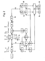
- FIG. 2 shows the block diagram of a discriminator for performing the method.
- detector pulses 2 are generated, which are used to compensate for signal attenuations caused by the construction of the detector, with a first integrated into detector 1
- Amplifier 3 are amplified, which has an output impedance of 50 ohms.
- the output A of the detector 1 is connected to a first comparator 7 with a predetermined first threshold S 1 and to a second comparator 8 with a predetermined second threshold S 2 > S 1 .
- the non-inverting output of the first comparator 7 is connected via a digital delay element 9, the inverting output of the second comparator 8 directly to a start circuit lo, which only triggers the start circuit lo when the amplitudes A of the detector pulse 2 exceed the second threshold S2.
- the output of the start circuit lo is switched to a level adjustment 11, which converts a change in the input signal from “O” to "1” into a voltage change from O to -5 volts.
- a gate time pulse generator 12 connected downstream of the level adjustment 11 generates gate time pulses 13 of predetermined, constant pulse width t 3 lying in the nanosecond range.
- the output of the gate time pulse generator 12 is connected to the control input of the electronic switch 6 which can be controlled by the gate time pulse 13 during the time t 1 .
- the time delay t 2 of the detector pulse is determined by the time delays of the components required for signal processing and is set by the delay line 4.
- the leading edge 14 of the gate time pulse 13 lies immediately before the delay time t 2 expires.
- the electronic switch 6 is blocked by the trailing edge 15 of the gate time pulse 13.
- the trailing edge 15 thus also determines the end of the time t provided for the time discrimination and stops the rising of the leading edge 5 of the detector pulse 2 at an amplitude value A ⁇ , A ⁇ .
- the electronic switch 6 is followed by a pulse shaper 16, which converts the signal voltages of the time-discriminated detector pulse 2 corresponding to the amplitudes A ⁇ , A ⁇ into an electrical charge of a capacitor and stretches the peak-shaped maximum value 17 of the amplitudes A ⁇ , A ⁇ obtained by the time discrimination .
- the output of the pulse shaper 16 is connected via a second amplifier 18 to the inputs of a third comparator 19 with a predetermined third threshold S 3 > S 2 and a fourth comparator 2o with a predetermined fourth threshold S 4 > S 3 .
- the inverting output of the third comparator 19 is on a fourth memory 21, the inverting.
- the output of the fourth comparator 2o is connected to a fifth memory 22.
- the outputs of the fourth memory 21 and the fifth memory 22 are connected to an evaluation logic 23 which sorts the time and amplitude-discriminated detector pulse into ⁇ signals, ⁇ signals and ⁇ or ⁇ signals.
- the evaluation logic 23 is followed by a first counter 24 for ⁇ signals, a second counter 25 for ⁇ signals and a third counter 26 for ⁇ or ⁇ signals.
- the inverting output of the first comparator 7 is followed by a timer 27, the output of which is connected to the evaluation logic 23.
- the timer At the end of the measuring time, the timer generates a read pulse for transferring the contents of the fourth memory 21 or the fifth memory 22 via the evaluation logic 23 into one of the counters 24, 25, 26.
- the inverting output of the first comparator 7 is followed by a reset logic 28, the second input is connected to the output of the timer 27 and its output is connected to the reset inputs of the memories, the reset logic 28, the start circuit 10 and the fourth and fifth memories 21, 22.
- Each of the stores consists of a bistable flip-flop.
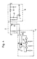
- FIG. 3 shows the circuit diagram of the comparators, the memories, the start circuit 10, the evaluation logic 23 and the reset logic 28.
- the start circuit lo generates only at the second threshold S 2 exceeding signal amplitudes Ay, A ⁇ at its output 3o a signal triggering the level adjustment 11.
- the starting circuit 10 consists of a second bistable multivibrator 31, a third bistable multivibrator 32, a second NAND gate 33 and a third NAND gate 34.
- the second bistable multivibrator 31 is connected downstream of the second NAND gate 33, the first input of which is connected to the output of the digital delay element 9 and the second input of which is connected to the inverting output of the second comparator 8.
- the non-inverting output 35 of the second flip-flop 31 is connected to the first input of the third NAND gate 34, the second input of which is connected to the non-inverting output of the second comparator 8.
- the output of the third NAND gate 34 is followed by the third bistable multivibrator 32, whose inverting output 3o is connected to the level adjustment 11.
- the level adjustment 11 consists essentially of a pnp transistor 36 whose base lo at the output of the starting circuit 3o, whose emitter auf.eine positive voltage of 5 volts, and the collector to a ne g a- tive voltage of 5 volts is switched.
- the output of the level adjustment 11 is connected via the point C of the circuit to the input of a sixth bistable multivibrator 37 of the gate time pulse generator 12 shown in FIG. 4.
- the inverting output 38 of the flip-flop 37 is connected via a driver stage 39 to the control electrode of the electronic switch 6 designed as a field effect transistor 40.
- the non-inverting output 41 of the sixth bistable multivibrator 37 is fed back to its reset input via a delay element 42 which determines the opening time t 3 of the FET 40.
- the falling edge of the control signal generated by the level adjustment 11 triggers the sixth bistable multivibrator 37, whose inverting output 38 switches from -5 volts to 0 volts and thereby generates the leading edge 14 of the gate time pulse 13 shown in FIG. 1.
- the non-inverting output 41 goes from 0 to -5 volts.
- This signal is fed back to the reset input by the delay element 42, delayed by the time t 3 , and generates the trailing edge 15 of the gate time pulse 13, which determines the opening time t 3 of the electronic switch 6.
- a downstream integrating element 44 causes a temporal expansion of the peak-shaped maximum value 17 of the pulse amplitudes AO (, A ⁇ obtained by the time discrimination, which transmit the second amplifier 18 and the point B of the circuit via the point E of the circuit to the part of the circuit arrangement which effects the amplitude discrimination will.
- the non-inverting output 45 of the fourth memory 21 designed as a bistable multivibrator is connected to a first input of a first AND gate 46, the inverting output 47 is connected to a first input of a second AND gate 48, the second input of which is connected to the non-inverting output 49 of the fifth Memory 22 is switched.
- the inverting output 50 of the fifth memory 22 is connected to a first input of a third AND gate 51.
- the output of the second AND gate 48 is connected to a first input of a fourth AND gate 52.
- the second input of the first AND gate 46, the second input of the third AND gate 51 and the second input of the fourth AND gate 52 are connected to the output of the timer 27.
- the output of the first AND gate 46 is on a second counter 25 counting the B events
- the output of the third AND gate 51 is on a first counter 24 counting the ⁇ events
- the output of the fourth AND gate 52 is on a third counter 26, which counts neither the .alpha. or .beta.
- the first to fourth AND gates 46, 48, 51, 52 form the evaluation logic 23.
- the inverting output of the first comparator 7 is followed by a first monostable multivibrator 53 and this is followed by a second monostable multivibrator 54; the two flip-flops form the timer 27.
- the output of the timer 27 is connected to the input of a first bistable flip-flop 55, the inverting output 56 of which is connected to the first input of a first NAND gate 57.
- the second input of the first NAND gate 57 is connected to the inverting output of the first comparator 7.
- the output of the first NAND gate 57 is connected to the reset inputs of the first to fifth bistable flip-flops 55, 31, 32, 21, 22.
- the first bistable multivibrator 55 and the first NAND gate 57 form the reset logic 28.
- the second input of the second NAND gate 33 which is connected to the inverting output of the second comparator 8, remains at '1', so that the output of the second NAND gate 33 and thus the input of the second bistable multivibrator 31 and its non-inverting Output changes from '1' to '0'.
- the first input of the third NAND gate 34 thus goes to '0', the second input remains to 'O' and the output remains to '1', so that the inverting output of the third memory 32 remains at 'O' and the start circuit lo does not initiate a measurement process with time and amplitude discrimination.
- the inverting output of the first comparator 7 changes simultaneously from '1' to '0'.
- the falling edge triggers the first monostable multivibrator 53 and this, with a time delay, triggers a second monostable multivibrator 54 of the timing element 27, the output of which is connected to the first input of the first AND gate 46 of the evaluation logic 23.
- the second input of the first AND gate 46 is at '1', so that only the second counter 25 connected downstream of the first AND gate 38 for ⁇ signals receives a counting pulse from the '1' signal of the timing element 27.
- the level adjustment 11 converts the trigger pulse of the start circuit lo into a voltage change from 0 volts to -5 volts.
- This falling edge sets the sixth bistable multivibrator 37, which operates with an operating voltage of 0 and -5 volts.
- the inverting output 38 changes from -5 volts to 0 volts and generates the front edge 14 of the gate time pulse 13 that opens the switch 6 (see FIG. 1).
- the non-inverting output 41 resets the flip-flop after a time t 3 of approximately 3ns which can be determined by the delay element 42.
- the trailing edge 15 of the gate time pulse 13, which closes the switch 6, is generated.
- the time-discriminated detector signal is now discriminated in amplitude to determine the amplitude.
- A> S 4 unique ⁇ signal The inverting output of the fourth comparator 20 goes from '1' to '0', the inverting output 50 of the fifth memory 22 changes from '0' to '1'. Since the threshold S 1 has been exceeded, the first inputs of the first, third and fourth AND gates 46, 51, 52 are set to '1' via the output of the timing element 27. The output of the third AND gate thus goes to '1' and the first counter 24 counts an ⁇ pulse. The second and third counters 25, 26 do not receive a count pulse since the second inputs of the first and fourth AND gates 46, 52 connected upstream of the counter are at '0'.
- the positive pulse of the second monostable multivibrator 54 is thus used as a read signal for the fourth and fifth memories 21; 22 used.
- the time discrimination is running.
- the trailing edge of the pulse at the output of the second monostable multivibrator 54 ends the reading process of the fourth and fifth memories 21, 22 and simultaneously sets the inverted output 56 of the first bistable multivibrator 55 and the first input of the first NAND gate 57 to '1'. If its other input, which is connected to the inverting output of the first comparator 7, is also at '1', the output of the first NAND gate 57 goes to '0'.
- the first to fifth memories 55, 31, 32, 21, 22 are reset to a predetermined starting position and prepared for a new measurement.
- the combination of the output 56 of the first memory 55 with the inverting output of the first comparator 7 ensures that the reset pulse is only given to the memory if it is certain that the threshold S 1 of the first comparator 7 has not been exceeded, that is to say, itself no detector signal 2 is on the line.
- the pulse length of an ⁇ or ⁇ pulse is approx. 150 ns, the time required for a measurement is approx. 1.2 ⁇ s. Because of the statistical distribution of the pulses, one or more additional pulses can occur during a measurement. As soon as a measuring process is initiated by setting the third memory 32, further ⁇ or ⁇ pulses are therefore suppressed by the circuit until after the reset pulse their readiness for measurement is restored.
- Precondition for an exact measurement is that the reset pulse falls in time between two measurement signals, so that the measuring device is ready for operation when a detector signal 2 is received.
- the links in the circuit arrangement ensure that the time discrimination always begins with the rising front edge of the detector signal 2.
Landscapes
- Physics & Mathematics (AREA)
- Spectroscopy & Molecular Physics (AREA)
- Health & Medical Sciences (AREA)
- Life Sciences & Earth Sciences (AREA)
- General Physics & Mathematics (AREA)
- High Energy & Nuclear Physics (AREA)
- Molecular Biology (AREA)
- Manipulation Of Pulses (AREA)
- Measurement Of Radiation (AREA)
- Measurement Of Unknown Time Intervals (AREA)
Priority Applications (4)
| Application Number | Priority Date | Filing Date | Title |
|---|---|---|---|
| EP81103119A EP0063624B1 (fr) | 1981-04-25 | 1981-04-25 | Procédé et circuit pour la discrimination de particules alpha et bêta |
| DE8181103119T DE3173230D1 (en) | 1981-04-25 | 1981-04-25 | Method and circuit for the discrimination of alpha and beta particles |
| US06/283,189 US4454587A (en) | 1981-04-25 | 1981-07-14 | Method and circuit arrangement for discriminating between pulses generated by alpha and/or beta radiators |
| JP57037872A JPS57179774A (en) | 1981-04-25 | 1982-03-10 | Method and device for selecting pulse by alpha particle and pulse by beta particle |
Applications Claiming Priority (1)
| Application Number | Priority Date | Filing Date | Title |
|---|---|---|---|
| EP81103119A EP0063624B1 (fr) | 1981-04-25 | 1981-04-25 | Procédé et circuit pour la discrimination de particules alpha et bêta |
Publications (2)
| Publication Number | Publication Date |
|---|---|
| EP0063624A1 true EP0063624A1 (fr) | 1982-11-03 |
| EP0063624B1 EP0063624B1 (fr) | 1985-12-18 |
Family
ID=8187678
Family Applications (1)
| Application Number | Title | Priority Date | Filing Date |
|---|---|---|---|
| EP81103119A Expired EP0063624B1 (fr) | 1981-04-25 | 1981-04-25 | Procédé et circuit pour la discrimination de particules alpha et bêta |
Country Status (4)
| Country | Link |
|---|---|
| US (1) | US4454587A (fr) |
| EP (1) | EP0063624B1 (fr) |
| JP (1) | JPS57179774A (fr) |
| DE (1) | DE3173230D1 (fr) |
Cited By (1)
| Publication number | Priority date | Publication date | Assignee | Title |
|---|---|---|---|---|
| DE3125978A1 (de) * | 1981-07-01 | 1983-01-20 | Laboratorium Prof. Dr. Rudolf Berthold, 7547 Wildbad | Verfahren und vorrichtung zum spezifischen nachweis von (alpha)-strahlen und/oder (beta)- und (gamma)-strahlen in proportional-zaehlrohren bei gegenwart jeweils der anderen strahlungsart sowie anwendung |
Families Citing this family (10)
| Publication number | Priority date | Publication date | Assignee | Title |
|---|---|---|---|---|
| US5124936A (en) * | 1990-10-31 | 1992-06-23 | Science Applications International Corporation | Method and apparatus for measuring airborne uranium and transuranium elements |
| US5347129A (en) * | 1993-04-14 | 1994-09-13 | University Of Missouri-Columbia | System for determining the type of nuclear radiation from detector output pulse shape |
| US5475312A (en) * | 1994-06-07 | 1995-12-12 | Iris Power Engineering Inc. | Method and device for distinguishing between partial discharge and electrical noise |
| US6771712B2 (en) * | 2001-07-27 | 2004-08-03 | The Pulsar Network, Inc. | System for extracting a clock signal and a digital data signal from a modulated carrier signal in a receiver |
| CA2412488C (fr) | 2001-12-11 | 2009-09-08 | Crompton Gmbh | Procede de preparation d'hydrolysats partiels de catalyseurs a base de composes organometalliques ou de metaux de transition immobilises sur des supports inertes |
| DE102004009104A1 (de) * | 2004-02-25 | 2005-09-22 | Berthold Technologies Gmbh & Co. Kg | Verfahren und Vorrichtung zum Nachweis ionisierender Strahlung |
| US10031060B2 (en) | 2016-07-13 | 2018-07-24 | Mauro & Associates, Llc | Continuous, real time monitor for airborne depleted uranium particles in the respiratory range and corresponding method of use |
| CN109557573B (zh) * | 2018-11-29 | 2022-07-15 | 中广核久源(成都)科技有限公司 | 一种数字化的α/β射线甄别方法 |
| CN113075720B (zh) * | 2021-03-24 | 2024-05-31 | 福州智元仪器设备有限公司 | 一种基于组合式定时器的α、β射线甄别系统及方法 |
| CN115079244B (zh) * | 2022-06-30 | 2023-05-30 | 成都理工大学工程技术学院 | 一种基于下降沿幅值百分点斜率的数字n/γ甄别方法 |
Citations (1)
| Publication number | Priority date | Publication date | Assignee | Title |
|---|---|---|---|---|
| US4262203A (en) * | 1979-02-02 | 1981-04-14 | Overhoff Mario W | Alpha particle monitor |
Family Cites Families (7)
| Publication number | Priority date | Publication date | Assignee | Title |
|---|---|---|---|---|
| US3578960A (en) * | 1966-04-06 | 1971-05-18 | Beckman Instruments Inc | Radiation detection system with automatic sample counting rate determination |
| US3486025A (en) * | 1966-09-15 | 1969-12-23 | Lfe Corp | Apparatus for analyzing the energy distribution of a radioisotope in the presence of interfering radiation |
| US3638000A (en) * | 1966-10-07 | 1972-01-25 | Comitato Nazionale Per 1 En Nu | Method and apparatus for continuously determining the quantities of the qualitatively known radioactive nuclides contained in a physical system |
| US3717753A (en) * | 1969-10-01 | 1973-02-20 | Intertechnique Sa | Liquid scintillation spectrometer with automatic setting of channel limits |
| NL7110516A (fr) * | 1971-07-30 | 1973-02-01 | ||
| US3906377A (en) * | 1974-07-23 | 1975-09-16 | Us Navy | Pulse centroid detector |
| US4228512A (en) * | 1978-05-03 | 1980-10-14 | The Dow Chemical Company | Nuclear pulse counting apparatus and technique |
-
1981
- 1981-04-25 EP EP81103119A patent/EP0063624B1/fr not_active Expired
- 1981-04-25 DE DE8181103119T patent/DE3173230D1/de not_active Expired
- 1981-07-14 US US06/283,189 patent/US4454587A/en not_active Expired - Fee Related
-
1982
- 1982-03-10 JP JP57037872A patent/JPS57179774A/ja active Granted
Patent Citations (1)
| Publication number | Priority date | Publication date | Assignee | Title |
|---|---|---|---|---|
| US4262203A (en) * | 1979-02-02 | 1981-04-14 | Overhoff Mario W | Alpha particle monitor |
Non-Patent Citations (1)
| Title |
|---|
| Instruments and Experimental Techniques, Band 18, Nr. 6, Teil 1, November/Dezember 1975, seiten 1764-1767 New York, U.S.A. E.N. KUZIN et al.: "Devide for Identifying Recoil Protons According to the Shape of the Pulses in a Proportional Counter" * Abbildung 1a * * |
Cited By (1)
| Publication number | Priority date | Publication date | Assignee | Title |
|---|---|---|---|---|
| DE3125978A1 (de) * | 1981-07-01 | 1983-01-20 | Laboratorium Prof. Dr. Rudolf Berthold, 7547 Wildbad | Verfahren und vorrichtung zum spezifischen nachweis von (alpha)-strahlen und/oder (beta)- und (gamma)-strahlen in proportional-zaehlrohren bei gegenwart jeweils der anderen strahlungsart sowie anwendung |
Also Published As
| Publication number | Publication date |
|---|---|
| US4454587A (en) | 1984-06-12 |
| EP0063624B1 (fr) | 1985-12-18 |
| DE3173230D1 (en) | 1986-01-30 |
| JPS57179774A (en) | 1982-11-05 |
| JPH0315714B2 (fr) | 1991-03-01 |
Similar Documents
| Publication | Publication Date | Title |
|---|---|---|
| EP0063624B1 (fr) | Procédé et circuit pour la discrimination de particules alpha et bêta | |
| DE3039840C2 (de) | Zeitintervall-Meßvorrichtung | |
| DE1905176C3 (de) | Verfahren zur Analog-Digital-Umsetzung mit verbesserter Differentiallinearität der Umsetzung und Anordnung zur Durchführung dieses Verfahrens | |
| DE3419117A1 (de) | Optoelektrisches entfernungsmessgeraet mit einem zeitdiskriminator zur genauen ermittlung der zeitfolge elektrischer impulse | |
| DE1288632B (de) | Analog/Digital-Umsetzer mit einem Integrierverstaerker | |
| DE2847619C2 (fr) | ||
| DE2127283A1 (de) | Verfahren und Einrichtung zur Messung der Frequenz von elektrischen Signalen | |
| DE2728150C2 (de) | Analog/Digital-Umsetzer | |
| DE2503538A1 (de) | Geraet zum erzeugen eines zeitbezugssignals aus einem impuls von elektrischen signalschwingungen | |
| DE2235366B2 (de) | Schaltung zur unterdrueckung von signalen | |
| DE2653501B2 (de) | Frequenzvergleichsschaltung | |
| CH643972A5 (de) | Logarithmischer analog-digital-wandler. | |
| DE2150174A1 (de) | Vorrichtung zur Anzeige des Endes eines chromatographischen Signals | |
| DE3783893T2 (de) | Frequenz-spannungswandler. | |
| EP0942564A2 (fr) | Procedé pour détecter de signaux à impulsions | |
| DE2725618C3 (de) | Vorrichtung zur Messung des Integrals einer zeitabhängigen physikalischen Größe | |
| DE3322471A1 (de) | Messanordnung zur erfassung von strom- oder spannungswerten | |
| DE4222643A1 (de) | Einrichtung zur Messung von Pulslaufzeiten | |
| DE3322483A1 (de) | Messanordnung zur erfassung von strom- oder spannungswerten | |
| EP0141122B1 (fr) | Montage pour la mesure d'intervalles de temps courts | |
| DE3608440A1 (de) | Impulslaengen-diskriminator | |
| DE2803105C2 (fr) | ||
| DE2755492C2 (fr) | ||
| DE3612686A1 (de) | Verfahren und vorrichtung zur messung von zeitintervallen | |
| DE2203963B2 (de) | Schaltungsanordnung zur Verarbeitung von elektrischen Signalen |
Legal Events
| Date | Code | Title | Description |
|---|---|---|---|
| PUAI | Public reference made under article 153(3) epc to a published international application that has entered the european phase |
Free format text: ORIGINAL CODE: 0009012 |
|
| AK | Designated contracting states |
Designated state(s): BE CH DE FR GB NL |
|
| 17P | Request for examination filed |
Effective date: 19830321 |
|
| GRAA | (expected) grant |
Free format text: ORIGINAL CODE: 0009210 |
|
| AK | Designated contracting states |
Designated state(s): BE CH DE FR GB LI NL |
|
| REF | Corresponds to: |
Ref document number: 3173230 Country of ref document: DE Date of ref document: 19860130 |
|
| ET | Fr: translation filed | ||
| PLBE | No opposition filed within time limit |
Free format text: ORIGINAL CODE: 0009261 |
|
| STAA | Information on the status of an ep patent application or granted ep patent |
Free format text: STATUS: NO OPPOSITION FILED WITHIN TIME LIMIT |
|
| 26N | No opposition filed | ||
| PGFP | Annual fee paid to national office [announced via postgrant information from national office to epo] |
Ref country code: NL Payment date: 19870430 Year of fee payment: 7 |
|
| PG25 | Lapsed in a contracting state [announced via postgrant information from national office to epo] |
Ref country code: GB Effective date: 19890425 |
|
| PG25 | Lapsed in a contracting state [announced via postgrant information from national office to epo] |
Ref country code: LI Effective date: 19890430 Ref country code: CH Effective date: 19890430 Ref country code: BE Effective date: 19890430 |
|
| BERE | Be: lapsed |
Owner name: KERNFORSCHUNGSZENTRUM KARLSRUHE G.M.B.H. Effective date: 19890430 |
|
| PG25 | Lapsed in a contracting state [announced via postgrant information from national office to epo] |
Ref country code: NL Effective date: 19891101 |
|
| NLV4 | Nl: lapsed or anulled due to non-payment of the annual fee | ||
| GBPC | Gb: european patent ceased through non-payment of renewal fee | ||
| PG25 | Lapsed in a contracting state [announced via postgrant information from national office to epo] |
Ref country code: FR Free format text: LAPSE BECAUSE OF NON-PAYMENT OF DUE FEES Effective date: 19891228 |
|
| REG | Reference to a national code |
Ref country code: CH Ref legal event code: PL |
|
| REG | Reference to a national code |
Ref country code: FR Ref legal event code: ST |
|
| PGFP | Annual fee paid to national office [announced via postgrant information from national office to epo] |
Ref country code: DE Payment date: 20000404 Year of fee payment: 20 |