EP0066251A2 - Convertisseur numérique analogique - Google Patents
Convertisseur numérique analogique Download PDFInfo
- Publication number
- EP0066251A2 EP0066251A2 EP82104594A EP82104594A EP0066251A2 EP 0066251 A2 EP0066251 A2 EP 0066251A2 EP 82104594 A EP82104594 A EP 82104594A EP 82104594 A EP82104594 A EP 82104594A EP 0066251 A2 EP0066251 A2 EP 0066251A2
- Authority
- EP
- European Patent Office
- Prior art keywords
- digital
- analog
- dac
- output
- digital signal
- Prior art date
- Legal status (The legal status is an assumption and is not a legal conclusion. Google has not performed a legal analysis and makes no representation as to the accuracy of the status listed.)
- Granted
Links
- 238000006243 chemical reaction Methods 0.000 claims abstract description 18
- 238000010276 construction Methods 0.000 description 22
- 238000010586 diagram Methods 0.000 description 14
- 230000000295 complement effect Effects 0.000 description 7
- 101100115778 Caenorhabditis elegans dac-1 gene Proteins 0.000 description 5
- 238000005516 engineering process Methods 0.000 description 5
- 238000000034 method Methods 0.000 description 4
- 238000004519 manufacturing process Methods 0.000 description 3
- 239000011159 matrix material Substances 0.000 description 3
- 239000002131 composite material Substances 0.000 description 2
- 230000000694 effects Effects 0.000 description 2
- 238000002474 experimental method Methods 0.000 description 2
- 230000002349 favourable effect Effects 0.000 description 2
- 238000009966 trimming Methods 0.000 description 2
- 101100494437 Glycine max IFS2 gene Proteins 0.000 description 1
- 101100494439 Glycyrrhiza uralensis CYP93C2 gene Proteins 0.000 description 1
- 101100140586 Saccharomyces cerevisiae (strain ATCC 204508 / S288c) NAM7 gene Proteins 0.000 description 1
- 230000000536 complexating effect Effects 0.000 description 1
- 230000012447 hatching Effects 0.000 description 1
- 230000001629 suppression Effects 0.000 description 1
Images


Classifications
-
- H—ELECTRICITY
- H03—ELECTRONIC CIRCUITRY
- H03M—CODING; DECODING; CODE CONVERSION IN GENERAL
- H03M1/00—Analogue/digital conversion; Digital/analogue conversion
- H03M1/10—Calibration or testing
-
- H—ELECTRICITY
- H03—ELECTRONIC CIRCUITRY
- H03M—CODING; DECODING; CODE CONVERSION IN GENERAL
- H03M1/00—Analogue/digital conversion; Digital/analogue conversion
- H03M1/66—Digital/analogue converters
- H03M1/74—Simultaneous conversion
Definitions
- the present invention relates to a digital to analog converter (hereinafter abbreviated as DAC).
- DAC digital to analog converter
- the analog to digital converter comprises means for receiving an input digital signal of a first number of bit length, means for dividing the input digital signal to a plurality of digital signals of a second smaller number of bit length, the total value of the divided digital signals being equal to the valve of the input digital signals, a plurality of conversion means for converting the divided digital signals to analog signals, respectively, and means for summing the analog signals in value, in which the summed analog signal corresponds to the input digital signal.
- the respective conversion means have different conversion characteristics, e. g. different gain factors, such conversion means operate in parallel as a whole and in a repeated order, and hence the respective inherent conversion characteristics of the conversion means are neutralized.
- the relation between the summed analog signal and the input digital signal can be made substantially linear.
- the respective conversion means do not require a relatively high resolution and high linearity, and hence they can be fabricated with ease by known integrated circuit technology.
- known digital to analog converters may be used.
- a digital to analog converter comprising first setup means for deriving more significant N- bits as second data among first data consisting of N bits as second data, arithmetic means for adding the second data to the least significant bit of the first data thereby to generate third data, second setup means'for deriving the output of the arithmetic means as third data, first application means for applying the second data to a first basic DAC, second application means for applying said third data to a second basic DAC, and adder means for adding the respective outputs of the first and second basic DAC's to each other, the first data being an input of the digital-analog converter, and the output of the adder means being a converted output of the digital-analog converter.
- N represents a positive integer of 2 or.more.
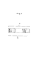
- First data (A) of N-bit are held, in an input register 1.
- the more significant (N-1) -bit data 1' including the most significant bit (MSB) to the (n-1)-th significant bit form second data (B).
- These second data (B) are held in a register 2 and transferred to a first DAC 8.
- the least significant (LSB) 1" of the aforementioned N-bit data (A) is transferred to an arithmetic circuit 3 jointly with the second data (B) to be added together, and new (N-l)-bit data are derived therefrom as third data (c).
- These third data (C) are temporarily held in a register 4 and transferred to a second DAC 9.
- FIG. 3 A code correlation diagram indicating the correlation between the input and output data of the arithmetic circuit illustrated in Fig. 1, is shown in Fig. 3.
- N 9 is assumed, and hence correlation between 9-bit input data (A) and 8-bit operated output data (B) and (C) is illustrated.
- the 8-bit output data (B) and (C) increase alternately by an increment of 1. For instance, when the analog value is 0, the data (A) are 000000000, and hence the data (B) and (C) are both 00000000.
- Fig. 4 is shown one preferred embodiment of the (B)+ (LSB) arithmetic circuit 3 in Fig. 1.
- the circuit 3 is composed of 9 digits of unit adder circuits AD 1 to AD 9 .
- Each of the unit adder circuits includes an exclusive- OR circuit composed of AND gates 41 and 42, inverter circuits 44 and 45 and an OR gate 43 and a carry circuit composed of an AND gate 46.
- the bits A 1 to A 8 forming the more significant (N-1) data are treated as the data (B) composed of bits B 0 to B ⁇ .
- the data (C) is obtained by adding LSB A o of the data (A) to the data (B), and hence the respective bits C o to C 7 are derived from the respective exclusive-OR circuits of the unit adder circuits AD 1 to AD 9 .
- the bit A 0 as the LSB of the data (A) and the bit A 1 corresponding to the LSB of the data (B) are applied.
- the respective bits A 2 to A 8 as the remainding bits of the data (B) are applied which are added with the carry signal supplied from the carry circuits from the previous bit positions, respectively.
- Fig. 5 is shown another preferred embodiment of the present invention in which arithmetic units such as micro-processors or the like are employed.
- a micro-processor 21 arithmetic operations according to the data flow shown in Fig. 1 are effected, the results of operations are placed on a data bus 13 through an output port 22 to effect writing of data in the DAC designated by control data which are placed on an address bus 18 and decoded by an address decoder 19.
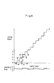
- the system uses four basic DAC's consisting of DAC(A) through DAC (D] .
- the data blocks (B) and (C) derived as indicated in Fig.
- the outputs the basic DAC's DAC [A], DAC [B], DAC[C] and DAC[D] are sequentially incremented by one in accordance with the continuous increase of the digital input (data ( A)).
- the basic DAC DAC [A] produces an analog output of "1” in response to the digital input " .... 001"
- the gain factor of DAC[A] is 0. 7 and hence the analog output 30 at this instance is smaller than the specified analog output 30' corresponding "1" by 0.3.
- the DAC [B] is enabled to produce the analog output of "1" as well as the DAC [A].
- the output of the DAC [B] is added to the output of the DAC (A] to generate the analog output of "2" as indicated by 31.
- the gain factor of the DAC [B] is 1 and hence the analog output 31 thus obtained is smaller than the specified value of "2" indicated by 31' by 0.3..
- the digital input is "...1011”
- the output corresponding to "1" value from the DAC [C] is also added to the outputs of the DAC [A] and the DAC [B].
- the gain factor of the DAC[C] is 1.4, and hence the analog output 32 takes a larger value than the specified "3" value 32' by 0.1. Then, the digital input becomes "..
- the output of the DAC [D] is added to the outputs of the DAC [A] , DAC [B] and DAC [C] .
- the analog output 33 corresponds to the specified value of "4".
- a digital-analog converter such as the first and second basic DAC's 8 and 9 in Fig. 1 or the basic DAC [A] to DAC [D] in Fig. 5.
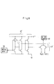
- Fig. 7 shows one example of the structure of the basic DAC.
- the so-called R-2R ladder circuit is used, in which a resistor 53(R) in a first group is chosen to be 10K ⁇ and a resistor 54 (2R) in a second group is chosen to be 20 K ⁇ .
- another resistor 55 in a feedback impedance circuit is chosen to be 10 K ⁇ .
- FET's of complementary MOS (hereinafter abbreviated as (MOS) type are used for a current switch group 51 and a drive circuit group 52.
- MOS complementary MOS
- the output for each bit of the resistor network 50 is connected to a movable contact of the corresponding switch in the current switch group 51, so that it may be terminated at either a first output I OUT1 or a second output I OUT2 depending upon digital inputs applied to an input circuit 56.
- the respective switches in this current switch group 51 are driven by the corresponding one of drive circuits 61 to 70 in the drive circuit group 52, and to the respective input terminals of the input circuit 56 are applied digital inputs A 1 to A 10 .
- the digital input A 1 is the most significant bit, while the digital input A 10 is the least significant bit, these inputs A 1 to A 10 form binary weight bits, and the current switch group 51 leads binary weighted currents either to the first output terminal I OUT1 or to the second output terminal I OUT2 .
- a current represented a totalized analog value is obtained by connecting the first output terminals I OUT1 of the respective basic DAC's together and also connecting the second output terminals I OUT2 of the respective basic .DAC's together.
- Fig. 8 shows a circuit portion 52' and 51' for arbitrary one bit in the drive circuit group 52 and the current switch group 51 in Fig. 7.
- the current switch portion 51' is composed of two FET's of the same conductivity type, and in the illustrated case they are both N-channel FET's.
- V + To the gate of one FET that is conducting in this current switch 51' is applied a voltage V + from the drive circuit 52', whereas the ground potential is applied to the gate of the FET that is non-conducting.
- one output terminal of the ladder resistor network 50 is connected either to the output terminal IOUT1 or to the output terminal I OUT2 by one FET that is then conducting.
- the DAC illustrated in Figs. 7 and 8 is favorable to be used as the basic DAC shown in Fig. 1 or in Fig. 5.
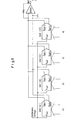
- FIG. 9 One example of a circuit arrangement for employing four such DAC's practically as the DAC [A] to DAC[D] in Fig. 5 is illustrated in Fig. 9.
- the corresponding output terminals I OUT1 or I OUT2 of the respective DAC's are connected in common and connected to the corresponding input terminal of an adder-amplifier, and the output of the amplifier is derived as an added output.
- To the respective DAC's (A] - (D) are applied four sets of divided data [a] - [d], respectively, and the output currents of the respective DAC's are added together by the above-mentioned adder-amplifier, from which the total sum of the output currents is derived.
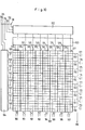
- Fig. 10 is a 6-bit DAC, in which depending upon the signals for the more significant 3 bits, the input-output range of the DAC can be equally divided into 8 segments.
- a segment #0 is allotted, and for the codes having the more significant 3 bits of "001" to "111", respectively, segments #1 to #7 are sequentially allotted.
- To the segment #0 belong 8 sets of codes consisting of "000000" to "000111”
- to the segment #1 belong 8 sets of codes consisting of "001000" to "001111”, and so on.
- the current source switch cells led to different ones of the complementary output terminals I 0 and I 0 are differentiated by different directions of hatchings.
- the outputs of all the current source switch cells included in the columns #4 to #7 to which outputs B 4 to B 7 at a high level among the outputs of the above-described second encoder 103 are applied, are led to the terminal I 0 independently of the outputs C o to C 7 of the third encoder 104.
- the current source switch cells included in the column #3 to which column the output B 3 at a low level of the second encoder 103 and the output A3 that is the only output held at a high level of the first encoder 102 are applied depend upon the outputs C o to C 7 of the third encoder 104 in such manner that the outputs of the current source switch cells included in the rows #0 to #5 to which outputs Co to C 5 at a low level are applied, are led to the terminal I 0 , while the outputs of the current source switch cells included in the row #6 and #7 to which the other outputs C 0 and C 7 . held at a high level are applied, are led to the terminal I 0 .
- the outputs of the current source switch cells included in the columns #0 to #2 to which columns the outputs A 0 - A 2 of the first encoder 102 and the outputs B 0 to B 2 of the second encoder 103 both held at a low level are applied are all led to the terminal I 0 independently of the outputs C o to C 7 of the third encoder 104 .
- a current source switch cell is not disposed at the position of row #7 and column #7.
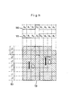
- a complementary output type DAC in some cases it is necessary to make the I 0 output zero for the input code of "111111". In such cases, the current source switch cell at the position of row #7 and column #7 can be omitted in practice as shown in Fig. 11.
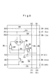
- a basic circuit construction 200 of the current source switch cell is illustrated in Fig. 12.
- This example of a current source switch cell relates to a switch cell adapted to make ON-OFF operations, and it is suitable for use in the cell group 100 in the example of the basic DAC shown in Fig. 11.
- a power supply wiring 280 can be automatically connected through terminals 281 and 282 to current source switch cells disposed at the adjacent positions.
- a ground wiring 270 is connected to a source of a FET 290 and connected through terminals 271 and 272 to the adjacent cells.
- a wiring 260 for feeding a gate bias voltage which is connected to the gate of the FET 290 and connected through terminals 261 and 262 to the adjacent cells.
- An analog output wiring 250 is connected to a drain of a FET 291 and connected through terminals 251 and 252 to the adjacent cells.
- An output signal line 220 of the aforementioned first encoder 102 which is connected through terminals 221 and 222 to the adjacent cells.
- An output signal line 230 of the second encoder 103 which is connected through terminals 231 and 232 to the adjacent cells.
- An output signal line 240 of the third encoder 104 which is connected through terminals 241 and 242 to the adjacent cells.
- a current source FET 290 is biased in common through the wiring 260.
- every current source switch cell can switch ON and OFF a unit current, and there current source switch cells can jointly form a basic DAC whose input-output characteristics have a linear relation.
- the drain of the current source FET 290 is connected to the source of the switch FET 291.
- the gate of the switch FET 291 is biased by an output of a multi-input logic gate, that is an AND-NOR circuit designated by reference numerals 292 to 293.
- multi-input logic gate 292 to 293 various combinations of logic elements can be constructed depending upon the positive or negative logic level of the control signal, whether the FET's are of P-channel type or of N-channel type, and the like, but in the illustrated circuit, by way of example, an AND-NOR circuit construction is employed.
- a first input terminal of a 2-input AND circuit 293 is connected to an output signal line 220 of the first encoder 102, and a second input terminal of the same is connected to an output signal line 242 of the third encoder 104.
- the output of the 2-input AND circuit 293 is connected to a first input terminal of a 3-input NOR circuit 292, and a second input terminal of the 3-input NOR circuit 292 is connected to an output signal line 230 of the second encoder 103.
- a third input of the same is connected to a common junction between the drain of the current source FET 290 and the source of the switch FET 291.
- the inhibit state of the cell is released, and the output state of the cell is controlled by the output signals of the first and third encoders 102 and 104.
- the level of the output signal of the first encoder 102 applied to the first input terminal of the AND circuit 293 is at a low level, the output of the AND circuit 293 takes a low level regardless of the level of the output signal of the third encoder 104 that is applied to.
- the NOR circuit 292 acts as an inverter-amplifier having the third input terminal connected to a junction 295 as an input and the output 296 of the NOR circuit 292 as an output, so that the switch FET 291 is feedback-biased to be turned ON, and this switch cell outputs a current to the output line 250.
- the level of the output signal of the second encoder 103 is at a low level and thereby the inhibit state of the cell has been released, if the level of the output signal of the first encoder 102 applied to the first input terminal of the AND circuit 293 is inverted to a high level, then the output state of the cell is determined depending upon the level of the output signal of the third encoder 104 applied to the second input terminal of the AND circuit 293.
- the level at the second input terminal of the AND circuit 293 is a high level, the output of the AND circuit 293 becomes a high level, hence the output of the NOR circuit 292 is turned to a low level, thus the switch FET 291 is cut off, and therefore, the cell takes an OFF (inhibit) state.
- the output of the AND circuit 293 becomes a low level, so that the NOR circuit 292 acts as an inverter-amplifier having the terminal 295 as an input and the terminal as an output, hence the switch FET 291 is feedback-biased and thus turned ON, and therefore, this cell outputs a current to the output line 250.
- the current source switch cell illustrated in Fig. 12 can achieve the intended operation as a basic constitutive element of the DAC shown in Fig. 10. Moreover, this current source switch cell has greatly improved the output impedance without complexing the construction of the analog current switches in the prior art, and it provides a favorable embodiment of the present invention for realizing a DAC having an extremely excellent output compliance characteristic in the form of a monolithic integrated circuit.
- the output compliance characteristic of a DAC implies suppression characteristic of an output current variation for an voltage amplitude at an analog current output terminal, and it is one of fundamental characteristics of a current output type DAC. With a DAC having an insufficient output compliance characteristic, it is impossible to realize a satisfactory precision for a wide range of output terminal voltage amplitudes.
- the switch FET 291 and the current source FET 291 are formed in the same shape, and if transconductances of these FET's are represented to gm, their output impedances by To, the drain potential of the switch FET 291, that is, the potential at the output terminal by V 5 , the potential at the common junction 295 between the source of the switch FET 291 and the drain of the current source FET 290 by V 295 , the output current by I 5 and the gate bias voltage of the current source FET 290 by V G , then the output current I 5 can be approximated as follows: Then the output conductance is derived as follows: where (- ⁇ ) is the gain of the NOR circuit 292 acting as an inverter-amplifier.
- the output impedance (the reciprocal of the output conductance) obtained by making use of a simple differential current switch form in the prior art was (gm r o ) r o , and therefore, in the case of the cell shown in Fig. 12, a further improvement by a factor of ⁇ has been achieved. It has been well known by those skilled in the art that the gain ⁇ of an NOR circuit operating as an inverter-amplifier can be easily chosen at 10 or more. In the experiments conducted by the inventor of this invention, the variations of the output current for an amplitude of 10 V of the output voltage was 0.00375%, and hence the variation rate was 0.000375%/V.
- the value of the least significant bit (LSB) in a 12-bit DAC with respect to its full scale value is about 0.025%, and so, if an error corresponding to 1 LSB is tolerable, then in a DAC cmploying the current source switch cells according to the present invention, an amplitude of 64 V is tolerable.
- the performance is degrated by a factor of 1/ ⁇ . Since the gain ⁇ of the inverter-amplifier employed in our experiments was 16, in the case where the differential analog current switches in the prior art are employed, the tolerable output amplitude would be greatly reduced to 4 V.
- Fig. 13 shows a complementary output type current source switch cell according to another preferred embodiment of the present invention, in which an complementary output terminal (I 0 ), a differential switch MOS FET 298 and a NOR circuit 297 are added to the current source switch cell in Fig. 12.
- This preferred embodiment provides a current source switch cell that is suitable to be applied to a complementary output type DAC.
- Component parts common to Fig. 12 are given like reference numerals.
- the switch cell illustrated in Fig. 13 carries out a complementary output operation, and so, it is a circuit having an excellent performance equivalent to the cell shown in Fig. 12.
- the above-described differential linearity is very excellent.
- a differential nonlinearity error implies an error of a variation in an analog output in response to a change of 1 LSB (the least significant bit unit) in every step of the digital input covering the codes of "000000000” to "111111111” with respect to the ideal amount of variation in response to a change of 1 LSB.
- the digital-analog converter according to the present invention can provide effective circuit means for constructing a digital-analog converter having a higher resolution.
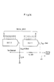
- Fig. 14 shows one example of application of the present invention to a high-precision digital-analog converter, in which the digital-analog converter according to the present invention whose linearity error and whose differential nonlinearity error are both small is used as a DAC for the more significant bits.
- a digital-analog converter DAC-1 according to the present invention is connected in correspondence to the more significant bit group in the digital input, and a digital-analog converter DAC-2 having any arbitrary construction is connected in correspondence to the less significant bit group, so that an analog voltage output may be derived between output terminals of a resistor network comprising resistors R 1 and R 2 .
- Fig. 15 shows another example of application of the present invention, in which for the resistor R 2 in the resistor network a variable resistor V R is used.
- a resolution can be raised by fine adjustment of the addition resistance ratio R l : R ⁇ .
- the optimum point can be obtained through a single adjustment operation of minimizing a high frequency distortion contained in an output derived by subjecting a digital coded since wave input to digital-analog conversion, and so, the adjustment work is very simple.
- any type of DAC is available, and for instance, the construction shown in Figs. 10 and 11 could be employed.
- Fig. 16 shows one example of a full-adder circuit for dividing 8-bit data at its input into 4 sets of 6-bit data to be applied to 4 basic DAC's as is the case with the example shown in Fig. 5 and Fig. 9. While various methods for dividing data can be conceived, in this figure is illustrated only one example.
- the digital-analog converter according to the present invention can provide a circuit arrangement for realizing a high- resolution digital-analog converter that can be mass-produced with a simple construction.
Landscapes
- Engineering & Computer Science (AREA)
- Theoretical Computer Science (AREA)
- Analogue/Digital Conversion (AREA)
Applications Claiming Priority (2)
| Application Number | Priority Date | Filing Date | Title |
|---|---|---|---|
| JP56080404A JPS57194625A (en) | 1981-05-27 | 1981-05-27 | Digital to analog converter |
| JP80404/81 | 1981-05-27 |
Publications (3)
| Publication Number | Publication Date |
|---|---|
| EP0066251A2 true EP0066251A2 (fr) | 1982-12-08 |
| EP0066251A3 EP0066251A3 (en) | 1985-12-11 |
| EP0066251B1 EP0066251B1 (fr) | 1988-12-28 |
Family
ID=13717345
Family Applications (1)
| Application Number | Title | Priority Date | Filing Date |
|---|---|---|---|
| EP82104594A Expired EP0066251B1 (fr) | 1981-05-27 | 1982-05-26 | Convertisseur numérique analogique |
Country Status (4)
| Country | Link |
|---|---|
| US (1) | US4503421A (fr) |
| EP (1) | EP0066251B1 (fr) |
| JP (1) | JPS57194625A (fr) |
| DE (1) | DE3279319D1 (fr) |
Cited By (1)
| Publication number | Priority date | Publication date | Assignee | Title |
|---|---|---|---|---|
| EP0249986A3 (fr) * | 1986-06-19 | 1991-07-03 | Nec Corporation | Convertisseur analogique-numérique |
Families Citing this family (46)
| Publication number | Priority date | Publication date | Assignee | Title |
|---|---|---|---|---|
| JPS5954322A (ja) * | 1982-09-22 | 1984-03-29 | Hitachi Ltd | D/a変換器 |
| JPS5956727A (ja) * | 1982-09-27 | 1984-04-02 | Fujitsu Ltd | 電子ビ−ム露光装置 |
| US4590457A (en) * | 1983-12-20 | 1986-05-20 | American Microsystems, Inc. | Digital to analog converter utilizing pulse width modulation |
| DE3516005A1 (de) * | 1985-05-03 | 1986-11-06 | Zdzislaw Medford Mass. Gulczynski | Digital-analog-wandler |
| JPS6376620A (ja) * | 1986-09-19 | 1988-04-06 | Matsushita Electric Ind Co Ltd | デイジタル−アナログ変換装置 |
| US4771267A (en) * | 1986-12-24 | 1988-09-13 | Hughes Aircraft Company | Analog offset compensation technique |
| US4766328A (en) * | 1987-05-26 | 1988-08-23 | System-General Corporation | Programmable pulse generator |
| DE3781277D1 (de) * | 1987-10-09 | 1992-09-24 | Ibm | Geraet zur aufloesungsausdehnung eines n-bit-ohmschen digital-analog-umsetzers in einen (n+p)-bit-digital-analog-umsetzer. |
| JPH01170119A (ja) * | 1987-12-24 | 1989-07-05 | Matsushita Electric Ind Co Ltd | ディジタル・アナログ変換装置 |
| JPH0697745B2 (ja) * | 1987-12-26 | 1994-11-30 | 岩崎通信機株式会社 | 多チャネル・デジタル・アナログ変換回路の制御方法 |
| US4926063A (en) * | 1988-11-14 | 1990-05-15 | Kollmorgen Corporation | Square root digital-to-analog converter |
| JP2683705B2 (ja) * | 1988-10-27 | 1997-12-03 | ナカミチ株式会社 | ディジタル/アナログ変換装置 |
| JPH02249310A (ja) * | 1988-12-14 | 1990-10-05 | Victor Co Of Japan Ltd | D/a変換装置 |
| JPH0334626A (ja) * | 1989-06-30 | 1991-02-14 | Yokogawa Electric Corp | D/a変換装置 |
| US4972188A (en) * | 1989-09-15 | 1990-11-20 | International Business Machines Corporation | Push pull double digital-to-analog converter |
| US5072358A (en) * | 1990-03-09 | 1991-12-10 | Daytronic Corporation | Process controller |
| US4998108A (en) * | 1990-07-30 | 1991-03-05 | International Business Machines Corporation | Large range, high speed, high accuracy digital-to-analog converter |
| US5451946A (en) * | 1993-06-28 | 1995-09-19 | Motorola Inc. | Apparatus and method for producing an analog output signal from a digital input word |
| DE4406326C1 (de) * | 1994-02-28 | 1995-02-16 | Ant Nachrichtentech | D/A-Wandler mit erhöhter Auflösung |
| US5568145A (en) * | 1994-10-19 | 1996-10-22 | Analog Devices, Inc. | MOS current source layout technique to minimize deviation |
| US6549942B1 (en) * | 1995-05-25 | 2003-04-15 | Audiohighway.Com | Enhanced delivery of audio data for portable playback |
| US5696988A (en) * | 1995-10-04 | 1997-12-09 | Ge Fanuc Automation North America, Inc. | Current/voltage configurable I/O module having two D/A converters serially coupled together such that data stream flows through the first D/A to the second D/A |
| KR100218329B1 (ko) * | 1996-11-08 | 1999-09-01 | 구본준 | 고속 저전력 디지탈 아날로그 컨버터 |
| GB2333171A (en) * | 1998-01-08 | 1999-07-14 | Fujitsu Microelectronics Ltd | Thermometer coding circuitry |
| GB2333408A (en) * | 1998-01-17 | 1999-07-21 | Sharp Kk | Non-linear digital-to-analog converter |
| FI105622B (fi) * | 1998-02-06 | 2000-09-15 | Nokia Networks Oy | Menetelmä suuren erottelukyvyn digitaali/analogia-muunnoksen suorittamiseksi ja digitaali/analogia-muunnin |
| SE519578C2 (sv) * | 1999-09-28 | 2003-03-18 | Ericsson Telefon Ab L M | D/A-omvandlingsförfarande och D/A-omvandlare |
| US6384750B1 (en) * | 2000-03-23 | 2002-05-07 | Mosaid Technologies, Inc. | Multi-stage lookup for translating between signals of different bit lengths |
| US7312739B1 (en) | 2000-05-23 | 2007-12-25 | Marvell International Ltd. | Communication driver |
| US7280060B1 (en) | 2000-05-23 | 2007-10-09 | Marvell International Ltd. | Communication driver |
| USRE41831E1 (en) | 2000-05-23 | 2010-10-19 | Marvell International Ltd. | Class B driver |
| US6775529B1 (en) | 2000-07-31 | 2004-08-10 | Marvell International Ltd. | Active resistive summer for a transformer hybrid |
| US7194037B1 (en) | 2000-05-23 | 2007-03-20 | Marvell International Ltd. | Active replica transformer hybrid |
| US6462688B1 (en) | 2000-12-18 | 2002-10-08 | Marvell International, Ltd. | Direct drive programmable high speed power digital-to-analog converter |
| US7113121B1 (en) | 2000-05-23 | 2006-09-26 | Marvell International Ltd. | Communication driver |
| US7433665B1 (en) | 2000-07-31 | 2008-10-07 | Marvell International Ltd. | Apparatus and method for converting single-ended signals to a differential signal, and transceiver employing same |
| US7095348B1 (en) | 2000-05-23 | 2006-08-22 | Marvell International Ltd. | Communication driver |
| US7606547B1 (en) * | 2000-07-31 | 2009-10-20 | Marvell International Ltd. | Active resistance summer for a transformer hybrid |
| DE50209650D1 (de) * | 2002-04-09 | 2007-04-19 | Infineon Technologies Ag | Vorrichtung zur Umwandlung eines digitalen Wertes in ein analoges Signal |
| EP1596625A1 (fr) * | 2004-05-11 | 2005-11-16 | AKG Acoustics GmbH | Circuit d'alimentation en signaux de haut-parleurs |
| US7312662B1 (en) | 2005-08-09 | 2007-12-25 | Marvell International Ltd. | Cascode gain boosting system and method for a transmitter |
| US7577892B1 (en) | 2005-08-25 | 2009-08-18 | Marvell International Ltd | High speed iterative decoder |
| DE602005016422D1 (de) * | 2005-10-11 | 2009-10-15 | Infineon Technologies Ag | Korrektur von statischen Fehlern durch Fehlanpassung in D/A-Umwandlern |
| TW200823853A (en) * | 2006-11-24 | 2008-06-01 | Novatek Microelectronics Corp | Source driving apparatus |
| US10069505B1 (en) * | 2017-09-13 | 2018-09-04 | Keysight Technologies, Inc. | Least significant bit dynamic element matching in a digital-to-analog converter |
| RU2703228C1 (ru) * | 2019-03-18 | 2019-10-15 | Юрий Александрович Никитин | Способ нониусного цифроаналогового преобразования |
Family Cites Families (11)
| Publication number | Priority date | Publication date | Assignee | Title |
|---|---|---|---|---|
| US3217147A (en) * | 1961-11-28 | 1965-11-09 | Bell Telephone Labor Inc | Cumulative type decoder |
| US3317905A (en) * | 1963-11-05 | 1967-05-02 | Gen Precision Inc | Data conversion system |
| US3588882A (en) * | 1969-08-04 | 1971-06-28 | Hughes Aircraft Co | Digital-to-analog converter |
| DE2536633A1 (de) * | 1974-11-15 | 1976-05-20 | Ibm | Digital-analogkonverter |
| US4016555A (en) * | 1975-04-07 | 1977-04-05 | Tyrrel Sylvan F | Signal converter |
| FR2357110A1 (fr) * | 1976-07-01 | 1978-01-27 | Trt Telecom Radio Electr | Systeme convertisseur numerique-analogique ayant une precision maximale en milieu d'echelle |
| JPS53132967A (en) * | 1977-04-26 | 1978-11-20 | Nippon Telegr & Teleph Corp <Ntt> | Da converter |
| JPS5492048A (en) * | 1977-12-29 | 1979-07-20 | Jeol Ltd | High resolution digital analogous convertr |
| JPS56153832A (en) * | 1980-04-30 | 1981-11-28 | Nec Corp | Digital to analog converter |
| US4412208A (en) * | 1980-09-16 | 1983-10-25 | Nippon Telegraph & Telephone Public Corporation | Digital to analog converter |
| US4430642A (en) * | 1981-10-02 | 1984-02-07 | Westinghouse Electric Corp. | Digital-to-analog converter |
-
1981
- 1981-05-27 JP JP56080404A patent/JPS57194625A/ja active Granted
-
1982
- 1982-05-26 US US06/382,189 patent/US4503421A/en not_active Expired - Lifetime
- 1982-05-26 DE DE8282104594T patent/DE3279319D1/de not_active Expired
- 1982-05-26 EP EP82104594A patent/EP0066251B1/fr not_active Expired
Cited By (1)
| Publication number | Priority date | Publication date | Assignee | Title |
|---|---|---|---|---|
| EP0249986A3 (fr) * | 1986-06-19 | 1991-07-03 | Nec Corporation | Convertisseur analogique-numérique |
Also Published As
| Publication number | Publication date |
|---|---|
| EP0066251A3 (en) | 1985-12-11 |
| EP0066251B1 (fr) | 1988-12-28 |
| JPS57194625A (en) | 1982-11-30 |
| JPS6225295B2 (fr) | 1987-06-02 |
| US4503421A (en) | 1985-03-05 |
| DE3279319D1 (en) | 1989-02-02 |
Similar Documents
| Publication | Publication Date | Title |
|---|---|---|
| EP0066251B1 (fr) | Convertisseur numérique analogique | |
| US5243347A (en) | Monotonic current/resistor digital-to-analog converter and method of operation | |
| EP0102609B1 (fr) | Convertisseur numérique-analogique | |
| EP0043897B1 (fr) | Circuit semi-conducteur | |
| EP0070175B1 (fr) | Convertisseur analogique-numérique | |
| US4594577A (en) | Current mirror digital to analog converter | |
| US5283580A (en) | Current/resistor digital-to-analog converter having enhanced integral linearity and method of operation | |
| US4338592A (en) | High accuracy digital-to-analog converter and transient elimination system thereof | |
| US6703956B1 (en) | Technique for improved linearity of high-precision, low-current digital-to-analog converters | |
| US4388612A (en) | Signal converter | |
| EP0325378B1 (fr) | Convertisseur numérique-analogique | |
| EP0141386B1 (fr) | Appareil de conversion numérique-analogique | |
| CA1259705A (fr) | Convertisseur numerique-analogique | |
| US4160244A (en) | Conversion circuit | |
| US5568145A (en) | MOS current source layout technique to minimize deviation | |
| EP0418184A1 (fr) | Convertisseur symétrique doublement numérique-analogique | |
| US4363024A (en) | Digital-to-analog converter providing multiplicative and linear functions | |
| EP0743758B1 (fr) | Convertisseur numérique-analogique quadratique | |
| EP1168628B1 (fr) | Convertisseur N/A du type à addition de courants | |
| JPH04162830A (ja) | D/aコンバータ | |
| US4658240A (en) | Apparatus for converting data between analog and digital values | |
| EP0329231A1 (fr) | Circuit de source de courant | |
| US5406285A (en) | Digital-to-analog converter | |
| US4727355A (en) | Digital-to-analog converter | |
| CA1243409A (fr) | Appareil de conversion analogique-numerique de donnees |
Legal Events
| Date | Code | Title | Description |
|---|---|---|---|
| PUAI | Public reference made under article 153(3) epc to a published international application that has entered the european phase |
Free format text: ORIGINAL CODE: 0009012 |
|
| AK | Designated contracting states |
Designated state(s): DE FR GB |
|
| RAP1 | Party data changed (applicant data changed or rights of an application transferred) |
Owner name: NEC CORPORATION |
|
| PUAL | Search report despatched |
Free format text: ORIGINAL CODE: 0009013 |
|
| AK | Designated contracting states |
Designated state(s): DE FR GB |
|
| 17P | Request for examination filed |
Effective date: 19860611 |
|
| 17Q | First examination report despatched |
Effective date: 19870223 |
|
| GRAA | (expected) grant |
Free format text: ORIGINAL CODE: 0009210 |
|
| AK | Designated contracting states |
Kind code of ref document: B1 Designated state(s): DE FR GB |
|
| REF | Corresponds to: |
Ref document number: 3279319 Country of ref document: DE Date of ref document: 19890202 |
|
| ET | Fr: translation filed | ||
| PLBE | No opposition filed within time limit |
Free format text: ORIGINAL CODE: 0009261 |
|
| STAA | Information on the status of an ep patent application or granted ep patent |
Free format text: STATUS: NO OPPOSITION FILED WITHIN TIME LIMIT |
|
| 26N | No opposition filed | ||
| PGFP | Annual fee paid to national office [announced via postgrant information from national office to epo] |
Ref country code: FR Payment date: 20010518 Year of fee payment: 20 |
|
| PGFP | Annual fee paid to national office [announced via postgrant information from national office to epo] |
Ref country code: DE Payment date: 20010522 Year of fee payment: 20 |
|
| PGFP | Annual fee paid to national office [announced via postgrant information from national office to epo] |
Ref country code: GB Payment date: 20010523 Year of fee payment: 20 |
|
| REG | Reference to a national code |
Ref country code: GB Ref legal event code: IF02 |
|
| PG25 | Lapsed in a contracting state [announced via postgrant information from national office to epo] |
Ref country code: GB Free format text: LAPSE BECAUSE OF EXPIRATION OF PROTECTION Effective date: 20020525 |
|
| REG | Reference to a national code |
Ref country code: GB Ref legal event code: PE20 Effective date: 20020525 |