EP0068882A2 - Kathodenstrahlanzeigeeinrichtung mit einer Schaltung zur Wiederordnung des Bildes - Google Patents
Kathodenstrahlanzeigeeinrichtung mit einer Schaltung zur Wiederordnung des Bildes Download PDFInfo
- Publication number
- EP0068882A2 EP0068882A2 EP82303390A EP82303390A EP0068882A2 EP 0068882 A2 EP0068882 A2 EP 0068882A2 EP 82303390 A EP82303390 A EP 82303390A EP 82303390 A EP82303390 A EP 82303390A EP 0068882 A2 EP0068882 A2 EP 0068882A2
- Authority
- EP
- European Patent Office
- Prior art keywords
- addresses
- address
- memory
- offset
- picture
- Prior art date
- Legal status (The legal status is an assumption and is not a legal conclusion. Google has not performed a legal analysis and makes no representation as to the accuracy of the status listed.)
- Granted
Links
Images
Classifications
-
- G—PHYSICS
- G09—EDUCATION; CRYPTOGRAPHY; DISPLAY; ADVERTISING; SEALS
- G09G—ARRANGEMENTS OR CIRCUITS FOR CONTROL OF INDICATING DEVICES USING STATIC MEANS TO PRESENT VARIABLE INFORMATION
- G09G1/00—Control arrangements or circuits, of interest only in connection with cathode-ray tube indicators; General aspects or details, e.g. selection emphasis on particular characters, dashed line or dotted line generation; Preprocessing of data
- G09G1/02—Storage circuits
Definitions
- the present invention relates to a cathode-ray tube (CRT) display device with a picture-rearranging circuit and more particularly to a full-graphic display device with a picture rearranging circuit.
- CTR cathode-ray tube
- a full-graphic display device is one which displays both words and pictures. It can display a great amount of visual data so that the operator can quickly respond to the data. For this reason, full-graphic display devices are widely used in picture-processing units, in electric power systems, in building-maintenance systems, in water supply systems, etc.
- a full-graphic display device comprises a memory for storing data to be displayed to a CRT display panel, an address counter for cyclically and sequentially generating count values so as to access the memory, and a microprocessing unit for controlling data to be written into the memory or for editing data stored in the memory so as to display a desired picture.
- the CRT display panel and the memory have panel addresses and memory addresses, respectively.
- the number of memory addresses is greater than the number of panel addresses.
- the microprocessing unit generates reading or writing addresses, for writing data into or reading data out of the memory, and also generates offset addresses.
- the offset addresses are used for rearranging the displayed picture on the display panel so that the picture is shifted rightwards, left-wards, upwards, downwards, or diagonally. Rearrangement of the picture is necessary when, for example, a great amount of data is to be displayed in a simple way and at a high speed.
- the offset addresses are calculated with other addresses by the address counter and by the microprocessing unit by using software.
- the use of software for calculating the offset address with other addresses greatly delays the operating speed of the address counter or the operating speed of the microprocessing unit. Therefore, the conventional system involves problems in that rearrangement of the picture is carried out at a slow speed and in that the speed at which the microprocessing unit controls to be written into or read out of the memory is slow.
- An embodiment of the present invention can provide a display device having a picture-rearranging circuit in which the speed at which the picture is rearranged is increased.
- An embodiment of the present invention can provide such a device as mentioned above in which the speed at which the microprocessing unit controls data to be written into or read out of the memory is increased.
- a display device having a picture-rearranging circuit and comprising: a memory. having memory addresses for storing data therein; a CRT display panel having panel addresses for displaying pictures corresponding to the data stored in the memory; a processor unit for generating writing or reading addresses and offset addresses for rearranging the picture displayed on said CRT display panel; an address counter for cyclically and sequentially generating count values; and a calculating circuit for calculating virtual addresses for acceessing the memory based on the count values and the writing or the reading addresses and the offset addresses.
- the advantages of the present invention are such that the address counter and the microprocessing unit need not calculate the offset address with other addresses. Therefore, as described later indetail, the processing time is greatly shortened.
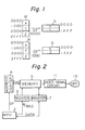
- Fig. 1 is a diagram explaining a general example of rearranging the displayed picture.
- M represents a memory
- D represents a CRT display panel.
- all addresses are expressed hexa-decimals.
- Memory M in this example, has a memory area ranging from address 0000 to address 2FFF.
- data X is stored between address 0000 and address OFFF; data Y is stored between address 1000 and lFFF; and data Z is stored between address 2000 and address 2FFF.
- the CRT display panel D in this example has panel addresses ranging from address 0000 to address IFFF.
- FIG. 2 is a block circuit diagram illustrating a main portion of a conventional CRT display device having a picture-rearranging circuit.
- 1 is a microprocessing unit for generating reading or writing addresses R/W AD and offset addresses OF and for processing data; 3 is an address register for temporarily storing the reading or writing addresses generated by microprocessing unit 1; 5 is a memory for storing data to be displayed; 7 is a data register for temporarily storing data output from microprocessing unit 1 or data read out of memory 5; 9 is an address counter for sequentially and cyclically generating display addresses; 11 is a video signal-generating circuit for converting data, read out of memory 5 by accessing the memory 5 by the display addresses from address counter 9 into video signals; and 13 is a CRT display unit. It is assumed that CRT display unit 13 has the same panel addresses ranging from address 0000 to address 1FFF as in Fig. 1.
- memory 5 has the same addresses ranging from address 0000 to address 2FFF as in Fig. 1.
- the number of display addresses generated during one cycle.of address counter 9 is the same as the number of panel addresses, i.e., 1FFF.
- Each cycle of address counter 9 is synchronous with one virtically synchronizing signal of CRT display unit 13.
- address counter 9 In a display operation when microprocessing unit 1 generates offset address 0000 to address counter 9, address counter 9 sequentially and cyclically generates display addresses from address 0000 to address 1FFF. These display addresses are the same as the count values originally generated by address counter 9. Thus, data stored in memory addresses 0000 to 1FFF is displayed.
- address counter 9 sequentially and cylically generates display addresses from-1000 to 2FFF.
- data stored in memory addresses ranging from 1000 to 2FFF is displayed on panel addresses ranging from 0000 to IFFF, respectively. Therefore, the picture is shifted upwards on the display panel by address 1000.
- the offset address is added to the count value originally generated by address counter 9 by software. This addition by software takes a long time, and, therefore, there is a disadvantage in that a long time is required to rearrange the picture.
- microprocessing unit 1 generates a writing address of 2001 and stores the new data in memory address 2001 of memory 5.
- the data displayed at a panel address of 1001 is rewritten.
- the generation of a reading or writing address is effected in microporcessing unit 1 by software. Therefore, a rewriting operation in which there is an offset takes a long time.
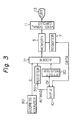
- FIG. 3 is a block circuit diagram illustrating a main portion of a CRT display device with a picture rearranging circuit, according to an embodiment of the present invention.
- 10 is a microprocessing unit for generating reading or writing addresses R/W AD and offset addresses OF and for processing data
- 20 is an offset registor for temporarily storing an offset address from microprocessing unit 10
- 21 is an adder
- 30 is an address register for temporarily storing a reading or writing address from microprocessing unit 10
- 90 is an address counter for sequentially and cyclically generating count values C.
- Memory 5, data register 7, video signal-generating circuit 11, and CRT display unit 13 are the same as those in the conventional device of Fig. 2.
- Adder 21 receives a reading or writing address R/W AD from address register 30, a count value C from address counter 90, and an offset address OF from offset register 20. It is assumed that CRT display unit 13 has panel addresses ranging from address 0000 to address 1FFF and that memory 5 has memory addresses ranging from address 0000 to address 2FFF. Address counter 90 sequentially and cyclically generates count values from 0000 to 1FFF. Each cycle of address counter 90 is synchronous with one virtically synchronizing signal of CRT display unit 13.
- microprocessing unit 10 In a display operation in which there is an offset address of 1000, microprocessing unit 10 generates offset address 1000 to offset register 20.
- Adder 21 adds each count value from address counter 90 and offset value 1000 from offset register 20 to form a virtual address, i.e., a display address for accessing memory 5.
- Adder 21, therefore, generates virtual addresses from 1000 to 2FFF in this case.
- data stored in memory addresses ranging from 1000 to 2FFF is displayed on panel addresses from 0000 to 1FFF, respectively.
- the picture is shifted on the display panel by address 1000. Since the display addresses are not obtained in address counter 90 by using software but instead are obtained in adder 21 by means of hardware, the time required for addition of the offset address is greatly shortened in comparison with that in the conventional device.
- Microprocessing unit 10 need not control address counter 90 since software in address counter 90 is unnecessary.
- Adder 21 adds reading address 1001 from address register 30 and offset address 1000 from offset register 20 so as to form a virtual address, i.e., new reading address 2001.
- Memory 5 is accessed by new reading address 2001 so that data stored in memory address 2001 is read into data register 7.
- Microprocessing unit 10 receives data from data registor 7 and processes the read data so as to generate new data to be rewritten.
- microprocessing unit 10 generates a writing address 1001 exactly corresponding to the panel address to be rewritten.
- Adder 21 again adds writing address 1001 and offset address 1000 so as to form a virtual address, i.e., new writing address 2001.
- the rewritten data is displayed at display address 1001 of display unit 13. Since microporcessing unit 10 need not calculate the new reading or writing address, the time required for the rewriting operation is also greatly shortened in comparison with the processing time in the conventional device.
- the present invention is not limited to the foregoing description of the embodiment.
- any number of panel addresses in the CRT display unit 13 or any number of memory addresses in the memory 5 is possible in the present invention.
- any type of calculating circuit may be substituted for adder 21. By using an appropriate calculating circuit, the picture on the display panel can be shifted not only upwards or downwards but also right wards or left wards and diagonally.
Landscapes
- Engineering & Computer Science (AREA)
- Radar, Positioning & Navigation (AREA)
- Remote Sensing (AREA)
- Physics & Mathematics (AREA)
- Computer Hardware Design (AREA)
- General Physics & Mathematics (AREA)
- Theoretical Computer Science (AREA)
- Controls And Circuits For Display Device (AREA)
Applications Claiming Priority (2)
| Application Number | Priority Date | Filing Date | Title |
|---|---|---|---|
| JP56100508A JPS582874A (ja) | 1981-06-30 | 1981-06-30 | フルグラフィックディスプレイ装置の画面構成変更回路 |
| JP100508/81 | 1981-06-30 |
Publications (3)
| Publication Number | Publication Date |
|---|---|
| EP0068882A2 true EP0068882A2 (de) | 1983-01-05 |
| EP0068882A3 EP0068882A3 (en) | 1983-03-30 |
| EP0068882B1 EP0068882B1 (de) | 1986-10-29 |
Family
ID=14275883
Family Applications (1)
| Application Number | Title | Priority Date | Filing Date |
|---|---|---|---|
| EP82303390A Expired EP0068882B1 (de) | 1981-06-30 | 1982-06-29 | Kathodenstrahlanzeigeeinrichtung mit einer Schaltung zur Wiederordnung des Bildes |
Country Status (5)
| Country | Link |
|---|---|
| US (1) | US4940970A (de) |
| EP (1) | EP0068882B1 (de) |
| JP (1) | JPS582874A (de) |
| DE (1) | DE3274027D1 (de) |
| IE (1) | IE53301B1 (de) |
Cited By (2)
| Publication number | Priority date | Publication date | Assignee | Title |
|---|---|---|---|---|
| DE3428099A1 (de) * | 1983-11-29 | 1985-06-05 | Mitsubishi Denki K.K., Tokio/Tokyo | Bildschirmsteuerung |
| EP0157254A3 (en) * | 1984-03-16 | 1987-01-21 | Ascii Corporation | Video display control system |
Families Citing this family (10)
| Publication number | Priority date | Publication date | Assignee | Title |
|---|---|---|---|---|
| US5075673A (en) * | 1989-06-16 | 1991-12-24 | International Business Machines Corp. | Variable speed, image pan method and apparatus |
| JP2531795B2 (ja) * | 1989-06-29 | 1996-09-04 | パイオニア株式会社 | 画像情報再生装置 |
| SE500157C2 (sv) * | 1989-09-13 | 1994-04-25 | Ericsson Telefon Ab L M | Förfarande för att välja basstation, radiokanal och tidslucka vid en mobilstation |
| US5229759A (en) * | 1991-08-23 | 1993-07-20 | Motorola Inc. | Auto-offset lcd vertical scroll mechanism |
| JPH0580815A (ja) * | 1991-09-19 | 1993-04-02 | Fanuc Ltd | Pcのメツセージ表示方式 |
| US5818417A (en) * | 1992-06-22 | 1998-10-06 | Vlsi Technology, Inc. | Automatic virtual display panning circuit for providing VGA display data to a lower resolution display and method therefor |
| US5628026A (en) * | 1994-12-05 | 1997-05-06 | Motorola, Inc. | Multi-dimensional data transfer in a data processing system and method therefor |
| US6008782A (en) * | 1995-05-05 | 1999-12-28 | Industrial Technology Research Institute | Mapping apparatus for use with a cathode-ray tube controller for generating special screen effects |
| US5774108A (en) * | 1995-06-21 | 1998-06-30 | Ricoh Company, Ltd. | Processing system with display screen scrolling |
| JP3517568B2 (ja) * | 1997-10-24 | 2004-04-12 | キヤノン株式会社 | 画像処理装置 |
Family Cites Families (11)
| Publication number | Priority date | Publication date | Assignee | Title |
|---|---|---|---|---|
| JPS5297632A (en) * | 1976-02-12 | 1977-08-16 | Hitachi Ltd | Display unit |
| US4068225A (en) * | 1976-10-04 | 1978-01-10 | Honeywell Information Systems, Inc. | Apparatus for displaying new information on a cathode ray tube display and rolling over previously displayed lines |
| US4246578A (en) * | 1978-02-08 | 1981-01-20 | Matsushita Electric Industrial Co., Ltd. | Pattern generation display system |
| US4201983A (en) * | 1978-03-02 | 1980-05-06 | Motorola, Inc. | Addressing circuitry for a vertical scan dot matrix display apparatus |
| DE2839888C2 (de) * | 1978-09-13 | 1982-06-03 | Siemens AG, 1000 Berlin und 8000 München | Schaltungsanordnung zum Darstellen von Symbolen auf dem Bildschirm eines Sichtgerätes |
| DE3067400D1 (en) * | 1979-01-15 | 1984-05-17 | Atari Inc | Apparatus for controlling a display |
| US4249172A (en) * | 1979-09-04 | 1981-02-03 | Honeywell Information Systems Inc. | Row address linking control system for video display terminal |
| JPS5858674B2 (ja) * | 1979-12-20 | 1983-12-26 | 日本アイ・ビ−・エム株式会社 | 陰極線管表示装置 |
| US4342991A (en) * | 1980-03-10 | 1982-08-03 | Multisonics, Inc. | Partial scrolling video generator |
| JPS5756885A (en) * | 1980-09-22 | 1982-04-05 | Nippon Electric Co | Video address control device |
| GB2130855B (en) * | 1982-11-03 | 1986-06-04 | Ferranti Plc | Information display system |
-
1981
- 1981-06-30 JP JP56100508A patent/JPS582874A/ja active Pending
-
1982
- 1982-06-29 EP EP82303390A patent/EP0068882B1/de not_active Expired
- 1982-06-29 IE IE1577/82A patent/IE53301B1/en unknown
- 1982-06-29 DE DE8282303390T patent/DE3274027D1/de not_active Expired
-
1989
- 1989-05-02 US US07/346,308 patent/US4940970A/en not_active Expired - Lifetime
Cited By (2)
| Publication number | Priority date | Publication date | Assignee | Title |
|---|---|---|---|---|
| DE3428099A1 (de) * | 1983-11-29 | 1985-06-05 | Mitsubishi Denki K.K., Tokio/Tokyo | Bildschirmsteuerung |
| EP0157254A3 (en) * | 1984-03-16 | 1987-01-21 | Ascii Corporation | Video display control system |
Also Published As
| Publication number | Publication date |
|---|---|
| US4940970A (en) | 1990-07-10 |
| EP0068882A3 (en) | 1983-03-30 |
| JPS582874A (ja) | 1983-01-08 |
| IE53301B1 (en) | 1988-10-12 |
| IE821577L (en) | 1982-12-30 |
| DE3274027D1 (en) | 1986-12-04 |
| EP0068882B1 (de) | 1986-10-29 |
Similar Documents
| Publication | Publication Date | Title |
|---|---|---|
| JP2853868B2 (ja) | フラットパネル表示システム | |
| US5592194A (en) | Display controller | |
| EP0068882A2 (de) | Kathodenstrahlanzeigeeinrichtung mit einer Schaltung zur Wiederordnung des Bildes | |
| US4935731A (en) | Image display apparatus | |
| US4484189A (en) | Memoryless artificial horizon generator | |
| EP0148575A2 (de) | Einrichtung und Verfahren zur gleichmässigen horizontalen Verschiebung für einer Videoanzeigegenerator | |
| US8026921B2 (en) | Driving method, driving circuit and driving apparatus for a display system | |
| JP3307736B2 (ja) | 画像データ転送装置 | |
| KR0161477B1 (ko) | 24bpp 모드에서의 메모리 매핑 방법 | |
| JPS6139092A (ja) | 表示装置 | |
| JPS60101587A (ja) | 表示メモリアクセス装置 | |
| JPS61219082A (ja) | 表示制御装置 | |
| JPS644187B2 (de) | ||
| JPS6195394A (ja) | 表示制御装置 | |
| JPH0795227B2 (ja) | 表示制御装置及び方法 | |
| JPH05297825A (ja) | 表示制御装置 | |
| JPS61122690A (ja) | 表示制御装置 | |
| JPS61130989A (ja) | X線画像処理装置 | |
| GB2136170A (en) | Method and apparatus for accessing a memory system | |
| JPS6143785A (ja) | 表示装置 | |
| JPH02154296A (ja) | 映像情報スクロール方式 | |
| JPH0495123A (ja) | 複数映像信号編集表示装置 | |
| JPS63229485A (ja) | 表示制御方式 | |
| JPS6195392A (ja) | 表示制御装置 | |
| JPS60177387A (ja) | Crt表示用大規模集積回路 |
Legal Events
| Date | Code | Title | Description |
|---|---|---|---|
| PUAI | Public reference made under article 153(3) epc to a published international application that has entered the european phase |
Free format text: ORIGINAL CODE: 0009012 |
|
| AK | Designated contracting states |
Designated state(s): DE FR GB |
|
| PUAL | Search report despatched |
Free format text: ORIGINAL CODE: 0009013 |
|
| AK | Designated contracting states |
Designated state(s): DE FR GB |
|
| 17P | Request for examination filed |
Effective date: 19830920 |
|
| GRAA | (expected) grant |
Free format text: ORIGINAL CODE: 0009210 |
|
| AK | Designated contracting states |
Kind code of ref document: B1 Designated state(s): DE FR GB |
|
| ET | Fr: translation filed | ||
| REF | Corresponds to: |
Ref document number: 3274027 Country of ref document: DE Date of ref document: 19861204 |
|
| PLBE | No opposition filed within time limit |
Free format text: ORIGINAL CODE: 0009261 |
|
| STAA | Information on the status of an ep patent application or granted ep patent |
Free format text: STATUS: NO OPPOSITION FILED WITHIN TIME LIMIT |
|
| 26N | No opposition filed | ||
| PGFP | Annual fee paid to national office [announced via postgrant information from national office to epo] |
Ref country code: GB Payment date: 19890531 Year of fee payment: 8 |
|
| PGFP | Annual fee paid to national office [announced via postgrant information from national office to epo] |
Ref country code: FR Payment date: 19890629 Year of fee payment: 8 |
|
| PGFP | Annual fee paid to national office [announced via postgrant information from national office to epo] |
Ref country code: DE Payment date: 19890824 Year of fee payment: 8 |
|
| PG25 | Lapsed in a contracting state [announced via postgrant information from national office to epo] |
Ref country code: GB Effective date: 19900629 |
|
| GBPC | Gb: european patent ceased through non-payment of renewal fee | ||
| PG25 | Lapsed in a contracting state [announced via postgrant information from national office to epo] |
Ref country code: FR Effective date: 19910228 |
|
| PG25 | Lapsed in a contracting state [announced via postgrant information from national office to epo] |
Ref country code: DE Effective date: 19910301 |
|
| REG | Reference to a national code |
Ref country code: FR Ref legal event code: ST |