EP0070071A1 - Zusammenbau mit einer gedruckten Schaltungskarte - Google Patents
Zusammenbau mit einer gedruckten Schaltungskarte Download PDFInfo
- Publication number
- EP0070071A1 EP0070071A1 EP82200839A EP82200839A EP0070071A1 EP 0070071 A1 EP0070071 A1 EP 0070071A1 EP 82200839 A EP82200839 A EP 82200839A EP 82200839 A EP82200839 A EP 82200839A EP 0070071 A1 EP0070071 A1 EP 0070071A1
- Authority
- EP
- European Patent Office
- Prior art keywords
- conducting particles
- printed circuit
- electrically conducting
- binder
- assembly
- Prior art date
- Legal status (The legal status is an assumption and is not a legal conclusion. Google has not performed a legal analysis and makes no representation as to the accuracy of the status listed.)
- Withdrawn
Links
Images
Classifications
-
- H—ELECTRICITY
- H01—ELECTRIC ELEMENTS
- H01R—ELECTRICALLY-CONDUCTIVE CONNECTIONS; STRUCTURAL ASSOCIATIONS OF A PLURALITY OF MUTUALLY-INSULATED ELECTRICAL CONNECTING ELEMENTS; COUPLING DEVICES; CURRENT COLLECTORS
- H01R12/00—Structural associations of a plurality of mutually-insulated electrical connecting elements, specially adapted for printed circuits, e.g. printed circuit boards [PCB], flat or ribbon cables, or like generally planar structures, e.g. terminal strips, terminal blocks; Coupling devices specially adapted for printed circuits, flat or ribbon cables, or like generally planar structures; Terminals specially adapted for contact with, or insertion into, printed circuits, flat or ribbon cables, or like generally planar structures
- H01R12/50—Fixed connections
- H01R12/59—Fixed connections for flexible printed circuits, flat or ribbon cables or like structures
- H01R12/62—Fixed connections for flexible printed circuits, flat or ribbon cables or like structures connecting to rigid printed circuits or like structures
-
- H—ELECTRICITY
- H01—ELECTRIC ELEMENTS
- H01R—ELECTRICALLY-CONDUCTIVE CONNECTIONS; STRUCTURAL ASSOCIATIONS OF A PLURALITY OF MUTUALLY-INSULATED ELECTRICAL CONNECTING ELEMENTS; COUPLING DEVICES; CURRENT COLLECTORS
- H01R12/00—Structural associations of a plurality of mutually-insulated electrical connecting elements, specially adapted for printed circuits, e.g. printed circuit boards [PCB], flat or ribbon cables, or like generally planar structures, e.g. terminal strips, terminal blocks; Coupling devices specially adapted for printed circuits, flat or ribbon cables, or like generally planar structures; Terminals specially adapted for contact with, or insertion into, printed circuits, flat or ribbon cables, or like generally planar structures
- H01R12/50—Fixed connections
- H01R12/59—Fixed connections for flexible printed circuits, flat or ribbon cables or like structures
- H01R12/65—Fixed connections for flexible printed circuits, flat or ribbon cables or like structures characterised by the terminal
- H01R12/67—Fixed connections for flexible printed circuits, flat or ribbon cables or like structures characterised by the terminal insulation penetrating terminals
-
- H—ELECTRICITY
- H01—ELECTRIC ELEMENTS
- H01R—ELECTRICALLY-CONDUCTIVE CONNECTIONS; STRUCTURAL ASSOCIATIONS OF A PLURALITY OF MUTUALLY-INSULATED ELECTRICAL CONNECTING ELEMENTS; COUPLING DEVICES; CURRENT COLLECTORS
- H01R12/00—Structural associations of a plurality of mutually-insulated electrical connecting elements, specially adapted for printed circuits, e.g. printed circuit boards [PCB], flat or ribbon cables, or like generally planar structures, e.g. terminal strips, terminal blocks; Coupling devices specially adapted for printed circuits, flat or ribbon cables, or like generally planar structures; Terminals specially adapted for contact with, or insertion into, printed circuits, flat or ribbon cables, or like generally planar structures
- H01R12/70—Coupling devices
- H01R12/71—Coupling devices for rigid printing circuits or like structures
- H01R12/712—Coupling devices for rigid printing circuits or like structures co-operating with the surface of the printed circuit or with a coupling device exclusively provided on the surface of the printed circuit
- H01R12/714—Coupling devices for rigid printing circuits or like structures co-operating with the surface of the printed circuit or with a coupling device exclusively provided on the surface of the printed circuit with contacts abutting directly the printed circuit; Button contacts therefore provided on the printed circuit
-
- H—ELECTRICITY
- H05—ELECTRIC TECHNIQUES NOT OTHERWISE PROVIDED FOR
- H05K—PRINTED CIRCUITS; CASINGS OR CONSTRUCTIONAL DETAILS OF ELECTRIC APPARATUS; MANUFACTURE OF ASSEMBLAGES OF ELECTRICAL COMPONENTS
- H05K3/00—Apparatus or processes for manufacturing printed circuits
- H05K3/30—Assembling printed circuits with electric components, e.g. with resistors
- H05K3/32—Assembling printed circuits with electric components, e.g. with resistors electrically connecting electric components or wires to printed circuits
- H05K3/321—Assembling printed circuits with electric components, e.g. with resistors electrically connecting electric components or wires to printed circuits by conductive adhesives
- H05K3/323—Assembling printed circuits with electric components, e.g. with resistors electrically connecting electric components or wires to printed circuits by conductive adhesives by applying an anisotropic conductive adhesive layer over an array of pads
-
- H—ELECTRICITY
- H01—ELECTRIC ELEMENTS
- H01R—ELECTRICALLY-CONDUCTIVE CONNECTIONS; STRUCTURAL ASSOCIATIONS OF A PLURALITY OF MUTUALLY-INSULATED ELECTRICAL CONNECTING ELEMENTS; COUPLING DEVICES; CURRENT COLLECTORS
- H01R13/00—Details of coupling devices of the kinds covered by groups H01R12/70 or H01R24/00 - H01R33/00
- H01R13/02—Contact members
- H01R13/22—Contacts for co-operating by abutting
- H01R13/24—Contacts for co-operating by abutting resilient; resiliently-mounted
- H01R13/2407—Contacts for co-operating by abutting resilient; resiliently-mounted characterized by the resilient means
- H01R13/2414—Contacts for co-operating by abutting resilient; resiliently-mounted characterized by the resilient means conductive elastomers
-
- H—ELECTRICITY
- H01—ELECTRIC ELEMENTS
- H01R—ELECTRICALLY-CONDUCTIVE CONNECTIONS; STRUCTURAL ASSOCIATIONS OF A PLURALITY OF MUTUALLY-INSULATED ELECTRICAL CONNECTING ELEMENTS; COUPLING DEVICES; CURRENT COLLECTORS
- H01R4/00—Electrically-conductive connections between two or more conductive members in direct contact, i.e. touching one another; Means for effecting or maintaining such contact; Electrically-conductive connections having two or more spaced connecting locations for conductors and using contact members penetrating insulation
- H01R4/04—Electrically-conductive connections between two or more conductive members in direct contact, i.e. touching one another; Means for effecting or maintaining such contact; Electrically-conductive connections having two or more spaced connecting locations for conductors and using contact members penetrating insulation using electrically conductive adhesives
-
- H—ELECTRICITY
- H01—ELECTRIC ELEMENTS
- H01R—ELECTRICALLY-CONDUCTIVE CONNECTIONS; STRUCTURAL ASSOCIATIONS OF A PLURALITY OF MUTUALLY-INSULATED ELECTRICAL CONNECTING ELEMENTS; COUPLING DEVICES; CURRENT COLLECTORS
- H01R4/00—Electrically-conductive connections between two or more conductive members in direct contact, i.e. touching one another; Means for effecting or maintaining such contact; Electrically-conductive connections having two or more spaced connecting locations for conductors and using contact members penetrating insulation
- H01R4/26—Connections in which at least one of the connecting parts has projections which bite into or engage the other connecting part in order to improve the contact
-
- H—ELECTRICITY
- H05—ELECTRIC TECHNIQUES NOT OTHERWISE PROVIDED FOR
- H05K—PRINTED CIRCUITS; CASINGS OR CONSTRUCTIONAL DETAILS OF ELECTRIC APPARATUS; MANUFACTURE OF ASSEMBLAGES OF ELECTRICAL COMPONENTS
- H05K2201/00—Indexing scheme relating to printed circuits covered by H05K1/00
- H05K2201/02—Fillers; Particles; Fibers; Reinforcement materials
- H05K2201/0203—Fillers and particles
- H05K2201/0206—Materials
- H05K2201/023—Hard particles, i.e. particles in conductive adhesive at least partly penetrating an electrode
-
- H—ELECTRICITY
- H05—ELECTRIC TECHNIQUES NOT OTHERWISE PROVIDED FOR
- H05K—PRINTED CIRCUITS; CASINGS OR CONSTRUCTIONAL DETAILS OF ELECTRIC APPARATUS; MANUFACTURE OF ASSEMBLAGES OF ELECTRICAL COMPONENTS
- H05K2201/00—Indexing scheme relating to printed circuits covered by H05K1/00
- H05K2201/10—Details of components or other objects attached to or integrated in a printed circuit board
- H05K2201/10007—Types of components
- H05K2201/10128—Display
- H05K2201/10136—Liquid Crystal display [LCD]
-
- H—ELECTRICITY
- H05—ELECTRIC TECHNIQUES NOT OTHERWISE PROVIDED FOR
- H05K—PRINTED CIRCUITS; CASINGS OR CONSTRUCTIONAL DETAILS OF ELECTRIC APPARATUS; MANUFACTURE OF ASSEMBLAGES OF ELECTRICAL COMPONENTS
- H05K2201/00—Indexing scheme relating to printed circuits covered by H05K1/00
- H05K2201/10—Details of components or other objects attached to or integrated in a printed circuit board
- H05K2201/10227—Other objects, e.g. metallic pieces
- H05K2201/10393—Clamping a component by an element or a set of elements
-
- H—ELECTRICITY
- H05—ELECTRIC TECHNIQUES NOT OTHERWISE PROVIDED FOR
- H05K—PRINTED CIRCUITS; CASINGS OR CONSTRUCTIONAL DETAILS OF ELECTRIC APPARATUS; MANUFACTURE OF ASSEMBLAGES OF ELECTRICAL COMPONENTS
- H05K3/00—Apparatus or processes for manufacturing printed circuits
- H05K3/36—Assembling printed circuits with other printed circuits
- H05K3/361—Assembling flexible printed circuits with other printed circuits
Definitions
- the invention relates to an assembly comprising at least one printed circuit board electrically connected one at printed wiring terminations by means of coupling means to one or more circuit canpo- nents.
- Known coupling means are inter alia printed circuit conductors on a flexible substrate, connector pairs or unilaterally metallized flexible strips of an insulating plastic material, which all require rather a considerable time to produce and/or to mount.
- the said flexible strip is provided with parallel conducting paths each having a width which is less than the conductor spacing of the printed conductors which must be electrically connected by means of the strip.
- the assembly is characterized in that the coupling means are in the form of a dispersion of electrically conducting particles in a non-conducting paste-like binder or a thermoplastic foil together with means for keeping the printed wiring terminations and electrical connections on the circuit canponent (s) in secure mutual contact with the electrically conducting particles, or that the coupling means are a cured adhesive in which electrically conducting particles are dispersed and that the electrically conducting particles electrically connect the circuit canponent (s) to the printed wiring terminations.
- the coupling means are in the form of a dispersion of electrically conducting particles in a non-conducting paste-like binder or a thermoplastic foil together with means for keeping the printed wiring terminations and electrical connections on the circuit canponent (s) in secure mutual contact with the electrically conducting particles, or that the coupling means are a cured adhesive in which electrically conducting particles are dispersed and that the electrically conducting particles electrically connect the circuit canponent (s) to the printed wiring terminations.
- the circuit components may be for example a printed circuit board, a liquid crystal display device or leadless components.
- the electrically conductive particles must preferably have such a hardness that they are capable of penetrating through an oxide layer on the metal of the wiring terminations.
- the minimum diameter of the particles must of course be at least as large as the maximum thickness of the oxide layer.
- a metal which hardly forms oxide on its surface, such as, for example, German silver (Cu-Ni-Zn in a weight ratio 60-18-22) softer particles may be used which are smeared over a portion of the surface, the particles consisting of, for example, Au on Pt. With due observance of this limit it is yet possible to contact very narrow conductor widths and conductor spacings without short-circuiting.
- the number of particles must be so great that the resistance of the compressed paste-like binder or foil in which the particles are dispersed is sufficiently low in the thickness direction.
- the binder in which the particles are dispersed may be a fat, an oil or a wax, for example paraffin, petroleum jelly, bees wax, lanoline etc.
- the hard, conducting particles may consist of tungsten, molybdenum, ruthenium, stainless steel, ruthenium oxide, glassy carbon etc.
- the concentration of the particles in the mixture is approximately 10-50% by weight.
- the binder consists of a curable adhesive, for example a thermoplastic adhesive of the acrylonitrile-butadiene type, modified with a curable component, such as phenol formaldehyde or an epoxy resin.
- the adhesive also performs the function of a means for keeping the elements to be bonded in intimate contact with eachother.
- the adhesive is cured after positioning.
- This embodiment is particularly interesting for the permanent provision of lead-less components on a printed circuit board.
- an embodiment is possible wherein hard, conducting particles are dispersed in a thermoplastic foil, consisting for example of polyvinyl chloride.
- the connecting means provide an excellent protection for the bonded parts. Repeatedly detaching the parts and connecting them again does not affect the protection against corrosion and the contact resistance surprisingly does not increase but even becomes lower.
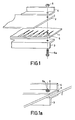
- reference numerals 1 and 2 denote printed circuit boards.
- the pattern of the printed circuit has a series of outputs which are provided on one side of the board in the form of parallel strips: that is to say, the series 5 on board 1 and a corresponding series, not shown, at the bottom side of board 2.
- the two series constitute a number of pairs of printed connectors.
- the edge areas of the boards on which the conducting strips are provided are coated with a conductive paste in accordance with the invention.
- Fig. 1a shows the combination after assembly;
- the boards are pressed each other by means of supporting strips 3 and 4, secured by nuts 6 engaged with bolts 6a.
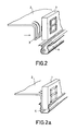
- Fig. 2 shows a liquid crystal board 1, the rear side of which is provided with a series of parallel outputs, not shown in this drawing.
- the flexible printed circuit foil 2 has a corresponding series of parallel outputs 3 of the printed circuit pattern, which is not shown in the drawing.
- the edge areas bearing the conducting strips of the two boards are coated with a conductive paste.
- Fig. 2 shows how the two parts are kept pressed together by means of a spring 4.
- the solution is cooled to a temperature at which is forms a jelly-like paste.
- the layers are applied by means of a brush or by dipping.
- the assemblies in accordance with these two embodiments are heated to arid maintained at 100°C and the resistance of the assemblies is measured after 24, 72 and 170 hours.
- the resistance is stable with a tendency to decrease.
Landscapes
- Engineering & Computer Science (AREA)
- Manufacturing & Machinery (AREA)
- Microelectronics & Electronic Packaging (AREA)
- Combinations Of Printed Boards (AREA)
- Conductive Materials (AREA)
- Parts Printed On Printed Circuit Boards (AREA)
- Adhesives Or Adhesive Processes (AREA)
Applications Claiming Priority (2)
| Application Number | Priority Date | Filing Date | Title |
|---|---|---|---|
| NL8103303 | 1981-07-10 | ||
| NL8103303A NL8103303A (nl) | 1981-07-10 | 1981-07-10 | Samengesteld lichaam. |
Publications (1)
| Publication Number | Publication Date |
|---|---|
| EP0070071A1 true EP0070071A1 (de) | 1983-01-19 |
Family
ID=19837772
Family Applications (1)
| Application Number | Title | Priority Date | Filing Date |
|---|---|---|---|
| EP82200839A Withdrawn EP0070071A1 (de) | 1981-07-10 | 1982-07-06 | Zusammenbau mit einer gedruckten Schaltungskarte |
Country Status (3)
| Country | Link |
|---|---|
| EP (1) | EP0070071A1 (de) |
| JP (1) | JPS5817691A (de) |
| NL (1) | NL8103303A (de) |
Cited By (8)
| Publication number | Priority date | Publication date | Assignee | Title |
|---|---|---|---|---|
| GB2123224A (en) * | 1982-06-30 | 1984-01-25 | Nippon Mektron Kk | Connecting circuit boards using conductive adhesive |
| EP0166627A1 (de) * | 1984-03-30 | 1986-01-02 | Boussois S.A. | Verbindung einer Schaltung auf einem starren Träger mit einer Schaltung auf mindestens einem biegsamen Träger |
| EP0268412A1 (de) * | 1986-11-10 | 1988-05-25 | Thomas & Betts Corporation | Flexibles Schaltkabel mit anisotropisch leitendem Klebstoff |
| EP0471148A3 (en) * | 1990-08-16 | 1993-06-02 | Technosales Company Establishment | Device for disconnecting and/or connecting of bus lines at a computer and circuit for a multiuser/multitask system with graphic capability |
| US5276817A (en) * | 1990-08-16 | 1994-01-04 | Technosales Company Establishment | System for splitting and connecting computer bus lines |
| EP0696092A3 (de) * | 1994-08-01 | 1996-10-02 | Sumitomo Electric Industries | Verbindungsanordnung für Stecker |
| EP0803558A3 (de) * | 1996-04-25 | 1998-10-21 | Lucent Technologies Inc. | Leitfähige Fixiereinlagen |
| DE10350568A1 (de) * | 2003-10-30 | 2005-02-10 | Ticona Gmbh | Verfahren zur Herstellung von Folienkabeln und Leiterbahnträgern für gedruckte Schaltungen sowie damit erhältliche gedruckte Schaltungen und Folienkabel |
Citations (5)
| Publication number | Priority date | Publication date | Assignee | Title |
|---|---|---|---|---|
| GB363075A (en) * | 1930-02-17 | 1931-12-17 | Vaw Ver Aluminium Werke Ag | A method of obtaining good contact between conductors of aluminium and its alloys |
| US3157735A (en) * | 1961-06-27 | 1964-11-17 | Aluminum Co Of America | Metallic particle compositions for mechanically joined electrical conductors |
| GB1161730A (en) * | 1967-10-23 | 1969-08-20 | Ncr Co | Electrical circuit controlling device |
| US4113981A (en) * | 1974-08-14 | 1978-09-12 | Kabushiki Kaisha Seikosha | Electrically conductive adhesive connecting arrays of conductors |
| EP0036226A1 (de) * | 1980-03-17 | 1981-09-23 | Koninklijke Philips Electronics N.V. | Elektrische Verbindungsmittel |
-
1981
- 1981-07-10 NL NL8103303A patent/NL8103303A/nl not_active Application Discontinuation
-
1982
- 1982-07-06 EP EP82200839A patent/EP0070071A1/de not_active Withdrawn
- 1982-07-07 JP JP57117033A patent/JPS5817691A/ja active Pending
Patent Citations (5)
| Publication number | Priority date | Publication date | Assignee | Title |
|---|---|---|---|---|
| GB363075A (en) * | 1930-02-17 | 1931-12-17 | Vaw Ver Aluminium Werke Ag | A method of obtaining good contact between conductors of aluminium and its alloys |
| US3157735A (en) * | 1961-06-27 | 1964-11-17 | Aluminum Co Of America | Metallic particle compositions for mechanically joined electrical conductors |
| GB1161730A (en) * | 1967-10-23 | 1969-08-20 | Ncr Co | Electrical circuit controlling device |
| US4113981A (en) * | 1974-08-14 | 1978-09-12 | Kabushiki Kaisha Seikosha | Electrically conductive adhesive connecting arrays of conductors |
| EP0036226A1 (de) * | 1980-03-17 | 1981-09-23 | Koninklijke Philips Electronics N.V. | Elektrische Verbindungsmittel |
Cited By (8)
| Publication number | Priority date | Publication date | Assignee | Title |
|---|---|---|---|---|
| GB2123224A (en) * | 1982-06-30 | 1984-01-25 | Nippon Mektron Kk | Connecting circuit boards using conductive adhesive |
| EP0166627A1 (de) * | 1984-03-30 | 1986-01-02 | Boussois S.A. | Verbindung einer Schaltung auf einem starren Träger mit einer Schaltung auf mindestens einem biegsamen Träger |
| EP0268412A1 (de) * | 1986-11-10 | 1988-05-25 | Thomas & Betts Corporation | Flexibles Schaltkabel mit anisotropisch leitendem Klebstoff |
| EP0471148A3 (en) * | 1990-08-16 | 1993-06-02 | Technosales Company Establishment | Device for disconnecting and/or connecting of bus lines at a computer and circuit for a multiuser/multitask system with graphic capability |
| US5276817A (en) * | 1990-08-16 | 1994-01-04 | Technosales Company Establishment | System for splitting and connecting computer bus lines |
| EP0696092A3 (de) * | 1994-08-01 | 1996-10-02 | Sumitomo Electric Industries | Verbindungsanordnung für Stecker |
| EP0803558A3 (de) * | 1996-04-25 | 1998-10-21 | Lucent Technologies Inc. | Leitfähige Fixiereinlagen |
| DE10350568A1 (de) * | 2003-10-30 | 2005-02-10 | Ticona Gmbh | Verfahren zur Herstellung von Folienkabeln und Leiterbahnträgern für gedruckte Schaltungen sowie damit erhältliche gedruckte Schaltungen und Folienkabel |
Also Published As
| Publication number | Publication date |
|---|---|
| JPS5817691A (ja) | 1983-02-01 |
| NL8103303A (nl) | 1983-02-01 |
Similar Documents
| Publication | Publication Date | Title |
|---|---|---|
| KR910005533B1 (ko) | 전기적 상호접속수단 및 접속방법 | |
| US4640981A (en) | Electrical interconnection means | |
| US4588456A (en) | Method of making adhesive electrical interconnecting means | |
| US4642421A (en) | Adhesive electrical interconnecting means | |
| US7625220B2 (en) | System for connecting a camera module, or like device, using flat flex cables | |
| US3731254A (en) | Jumper for interconnecting dual-in-line sockets | |
| JPH0850967A (ja) | 印刷プラスチツク回路および接触子とその製法 | |
| KR850008605A (ko) | 무선장치용 인쇄회로기판 및 회로조립체 | |
| KR840000080A (ko) | 혼성집적회로부품 및 그 부착방법 | |
| EP1347470A1 (de) | Elektrische Bauelemente mit leitfähigem Polymer | |
| KR100939607B1 (ko) | 회로의 접속 구조 및 접속 방법 | |
| EP0070071A1 (de) | Zusammenbau mit einer gedruckten Schaltungskarte | |
| EP0170703A1 (de) | Verbindungsstück in form eines films und dessen herstellungsverfahren | |
| EP1104046A3 (de) | Verfahren für Schaltungsaufbau und Schaltungsverbindungsanordnung in elektrischem Anschlusskasten | |
| JP2748615B2 (ja) | 導電性接着剤 | |
| US20030015349A1 (en) | Printed wiring board having wiring patterns and connection terminals | |
| JPH03196482A (ja) | 高圧電極 | |
| EP0198697A2 (de) | Adapter für einen gedruckten Leiterplattenverbinder | |
| US4708659A (en) | PC board connector with shorting bus bar | |
| EP0130462A3 (de) | Gedruckte Schaltung | |
| US3264596A (en) | Printed circuit board connector | |
| JP4080417B2 (ja) | エラストマコネクタ | |
| JPS5821391A (ja) | 電子部品の実装装置 | |
| JPS61133586A (ja) | コネクタ− | |
| JPS5855401Y2 (ja) | 表示装置 |
Legal Events
| Date | Code | Title | Description |
|---|---|---|---|
| PUAI | Public reference made under article 153(3) epc to a published international application that has entered the european phase |
Free format text: ORIGINAL CODE: 0009012 |
|
| 17P | Request for examination filed |
Effective date: 19820706 |
|
| AK | Designated contracting states |
Designated state(s): CH DE FR GB LI NL SE |
|
| STAA | Information on the status of an ep patent application or granted ep patent |
Free format text: STATUS: THE APPLICATION IS DEEMED TO BE WITHDRAWN |
|
| 18D | Application deemed to be withdrawn |
Effective date: 19840814 |
|
| RIN1 | Information on inventor provided before grant (corrected) |
Inventor name: VERWEG, FRANSISCUS G.C. Inventor name: STEINMETZ, ANTHONY Inventor name: ARNOLD, JACOBUS JOHANNES Inventor name: GERRITSEN, FREDERIK HENDRIK |