EP0071265A1 - Circuit comparateur MOS susceptible d'intégration monolithique - Google Patents
Circuit comparateur MOS susceptible d'intégration monolithique Download PDFInfo
- Publication number
- EP0071265A1 EP0071265A1 EP82106842A EP82106842A EP0071265A1 EP 0071265 A1 EP0071265 A1 EP 0071265A1 EP 82106842 A EP82106842 A EP 82106842A EP 82106842 A EP82106842 A EP 82106842A EP 0071265 A1 EP0071265 A1 EP 0071265A1
- Authority
- EP
- European Patent Office
- Prior art keywords
- inverter
- signal
- input
- output
- comparator
- Prior art date
- Legal status (The legal status is an assumption and is not a legal conclusion. Google has not performed a legal analysis and makes no representation as to the accuracy of the status listed.)
- Granted
Links
- 230000010354 integration Effects 0.000 title 1
- 238000012546 transfer Methods 0.000 claims abstract description 47
- 239000003990 capacitor Substances 0.000 claims abstract description 14
- 238000011156 evaluation Methods 0.000 claims description 7
- 239000004065 semiconductor Substances 0.000 claims description 3
- 238000000034 method Methods 0.000 claims description 2
- 238000010586 diagram Methods 0.000 description 4
- 230000009977 dual effect Effects 0.000 description 3
- 238000001208 nuclear magnetic resonance pulse sequence Methods 0.000 description 3
- 230000003321 amplification Effects 0.000 description 2
- 238000013461 design Methods 0.000 description 2
- 238000004519 manufacturing process Methods 0.000 description 2
- 238000005259 measurement Methods 0.000 description 2
- 238000003199 nucleic acid amplification method Methods 0.000 description 2
- 230000007704 transition Effects 0.000 description 2
- 230000000295 complement effect Effects 0.000 description 1
- 230000005611 electricity Effects 0.000 description 1
- 230000005669 field effect Effects 0.000 description 1
- 238000012913 prioritisation Methods 0.000 description 1
- 238000000926 separation method Methods 0.000 description 1
- 238000004904 shortening Methods 0.000 description 1
- 238000003860 storage Methods 0.000 description 1
- 230000001360 synchronised effect Effects 0.000 description 1
Images

Classifications
-
- G—PHYSICS
- G01—MEASURING; TESTING
- G01R—MEASURING ELECTRIC VARIABLES; MEASURING MAGNETIC VARIABLES
- G01R19/00—Arrangements for measuring currents or voltages or for indicating presence or sign thereof
- G01R19/165—Indicating that current or voltage is either above or below a predetermined value or within or outside a predetermined range of values
- G01R19/16504—Indicating that current or voltage is either above or below a predetermined value or within or outside a predetermined range of values characterised by the components employed
- G01R19/16519—Indicating that current or voltage is either above or below a predetermined value or within or outside a predetermined range of values characterised by the components employed using FET's
-
- H—ELECTRICITY
- H03—ELECTRONIC CIRCUITRY
- H03K—PULSE TECHNIQUE
- H03K5/00—Manipulating of pulses not covered by one of the other main groups of this subclass
- H03K5/22—Circuits having more than one input and one output for comparing pulses or pulse trains with each other according to input signal characteristics, e.g. slope, integral
- H03K5/24—Circuits having more than one input and one output for comparing pulses or pulse trains with each other according to input signal characteristics, e.g. slope, integral the characteristic being amplitude
- H03K5/2472—Circuits having more than one input and one output for comparing pulses or pulse trains with each other according to input signal characteristics, e.g. slope, integral the characteristic being amplitude using field effect transistors
- H03K5/249—Circuits having more than one input and one output for comparing pulses or pulse trains with each other according to input signal characteristics, e.g. slope, integral the characteristic being amplitude using field effect transistors using clock signals
-
- H—ELECTRICITY
- H03—ELECTRONIC CIRCUITRY
- H03M—CODING; DECODING; CODE CONVERSION IN GENERAL
- H03M1/00—Analogue/digital conversion; Digital/analogue conversion
- H03M1/12—Analogue/digital converters
- H03M1/34—Analogue value compared with reference values
- H03M1/36—Analogue value compared with reference values simultaneously only, i.e. parallel type
- H03M1/361—Analogue value compared with reference values simultaneously only, i.e. parallel type having a separate comparator and reference value for each quantisation level, i.e. full flash converter type
- H03M1/362—Analogue value compared with reference values simultaneously only, i.e. parallel type having a separate comparator and reference value for each quantisation level, i.e. full flash converter type the reference values being generated by a resistive voltage divider
Definitions
- the invention relates to a monolithically integrable MOS comparator circuit for comparing a signal voltage to be applied to the signal input of the comparator with the reference voltage to be applied to the reference input of the comparator, in which at least two amplifier stages connected in series and with respect to the supply voltage are provided.
- Comparator circuits of this type are common per se and can be designed in various ways.
- One possibility is to combine the two amplifier stages, each designed as an inverter, to form a flip-flop, which on one side e.g. is acted upon by the memory content of an addressed binary memory cell and on the other hand by the memory content of a reference cell designed and dimensioned in the same way as the memory cell.
- Another possibility is to use a comparator designed as a differential amplifier, the two branches of which are given by MOS transistors.
- comparators designed in this way are less suitable for use in fast analog-digital converters.
- fast analog-to-digital converters can be constructed from voltage comparators operating in parallel.
- a total of (2 n - 1) of such comparators is required in the case of an analog-digital converter operating in parallel operation with n bit resolution.
- this draws the disadvantage of a considerable space requirement in the circuit receiving semiconductor chips, unless you want to be satisfied with a small number of bits for the A / D converter.
- the known comparator cells lead to a considerable power requirement. It would therefore be desirable to design the individual comparator cells in such a way that they have a very small area requirement and require little electricity.
- the stroke of the measuring voltage of 3 V is large in comparison with the supply voltages of 3.5-5 V to be used for integrated circuits for known reasons.
- the comparator should be sufficiently fast and sensitive for the signal input voltage in this large range in order to be able to compare the input signal with the reference signal.
- a comparator corresponding to the definition given at the outset is designed such that the signal input and the reference input of the comparator are alternately connected to the same pole of a capacitor via a clock-controlled transfer transistor, the second pole of which is connected directly to the control input of a first amplifier stage designed as an inverter and is connected to the output of this first inverter via a further transfer transistor, that furthermore the output of this first inverter is connected via a fourth transfer transistor to the control input of a second amplifier stage, also designed as an inverter, and the output of this second inverter is used on the one hand as a signal output of the comparator and on the other hand is connected to the signal input of a third inverter which corresponds to the first and to the second inverter, the signal output of which is used both as the second signal output of the comparator and also as h is connected via a fifth transfer transistor to the control input of the second inverter, and in which finally the two clock signals switching the signal input or the reference input of the comparator to the
- the one clock signal can be identical to the clock signal switching the reference input to said capacitor and the other clock signal can be identical to the clock signal switching the signal input to the capacitor, as is the case with the circuit of the comparator according to the invention shown in FIG. However, it is also possible to swap the roles of the two clock sequences controlling the input transfer transistors when controlling the other transfer transistors.
- the invention is that a multi-stage, e.g. MOS amplifier implemented in n-channel technology is switched over in such a way that in a first clock phase all three amplifier stages (given by one of the inverters each) produce a high amplification factor in series, and that in a second clock phase the last two amplifier stages then form a flip- Flop are interconnected, which then amplifies the signal so far through its feedback that a logical decision is brought about and is effective as digital information on the output until the end of this clock phase.
- a multi-stage e.g. MOS amplifier implemented in n-channel technology is switched over in such a way that in a first clock phase all three amplifier stages (given by one of the inverters each) produce a high amplification factor in series, and that in a second clock phase the last two amplifier stages then form a flip- Flop are interconnected, which then amplifies the signal so far through its feedback that a logical decision is brought about and is effective as digital information on the output until the end of this
- the chain of three amplifier stages i.e. the three inverters, thus works in the sensitive range if the signal voltage is approximately equal to the reference voltage.
- the output voltage is set at the output of the amplifier chain, that is to say at the output of the third inverter, in accordance with the difference between the signal voltage and the reference voltage.
- the other clock phase during which the first inverter representing the first amplifier stage is fed back.
- the two subsequent amplifier stages are separated from the preliminary stage and fed back to a flip-flop via a transfer switch, which is given by the transfer transistor mentioned in fourth place in the definition of the invention.
- This flip-flop swings to digital levels very quickly and stores the information until the next measurement phase for the signal input voltage.
- An essential advantage of the arrangement according to the invention is that the time in which the first inverter stage is negative feedback is also used in the second and third inverter stages, namely for amplification and storage. Another advantage is that the double use of the second and third inverter stages saves space and power loss.
- An arrangement corresponding to the invention also shortens the time in which the output signal is available at the signal output of the flip-flop temporarily formed from the second and the third inverter.
- this digital signal is only for the transfer of the signal into the circuit to be applied by the comparator, e.g. priority logic and decoder; important, so that the shortening has no disadvantages.
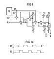
- FIG. 1 shows the circuit diagram of the comparator according to the invention
- FIG. 2 shows a block diagram for the use of the comparator according to the invention in a circuit for an analog-digital converter that works according to the parallel method.
- FIG. 1a shows the timing diagram for the operation of a comparator clock signals ⁇ 1 and 0 2 to be used according to the invention. You can, for example, by a clock generator TG. be delivered as described in DE-OS 27 13 319 (VPA 77 P 1027).
- the signal input SE of the comparator is connected to the same pole of a capacitor C via a first transfer transistor T1 and the reference input RE is connected via a second transfer transistor T2, which can be implemented, for example, as a MOS capacitor.
- the gate of the first transfer transistor T1 is controlled by the clock pulse sequence ⁇ 1 and the gate of the second transfer transistor T2 by the pulse sequence ⁇ 2 .
- the timing of these two pulse sequences ⁇ 1 and ⁇ 2 supplied by the clock generator TG is shown in Fig. 1a.
- the transfer transistors T1, T2 and the other transfer transistors T3 to T6 are of the normally-off type. The same applies to the driver transistors TT of the inverters 11, 12 and 13.
- the load transistors LT in the inverters in FIG. 1 are normally on. However, normally-off load transistors LT can also be used if the circuit is modified in a corresponding manner. In the example, all of the transistors are of the n-channel type, which, in the interest of a higher switching speed, is cheaper than the likewise possible use of p-channel MOS-FETs.
- the driver transistors TT, on the one hand, and the load transistors, on the other hand, and also the transfer transistors, are preferably each dimensioned the same, so that there is a minimum of relative tolerances during manufacture.
- the capacitor C which is acted upon by the signal input SE or the reference input RE, is, as can be seen from FIG. 1, with its other pole directly at the input of the inverter forming the first amplifier stage 11, which is given by the gate of the associated driver transistor TT. This is connected with its source connection to the reference potential O V and with its drain at the output of the inverter I1 and via the source-drain path of the load transistor LT of the inverter 11 connected as a diode to the first supply potential U.
- the output of the first inverter I1 leads via the third transfer gate T3 controlled by the reference clock ⁇ 2 back to the control input of the first inverter I1, that is to say to the gate of its driver transistor TT.
- the signal output of the first inverter I1 is also connected to the control input of the second inverter I2 and thus to the second amplifier stage of the comparator according to the invention via the fourth transfer transistor T4, which is controlled by the signal clock ⁇ 1 which connects the signal input SE to the capacitor C.
- the signal output of the second inverter I2 is, according to the definition of the invention, at the control input of a third inverter I3 and thus at the gate of the driver transistor TT of this inverter.
- the three inverters I1, I2, I3 are completely identical to one another in terms of their structure and in terms of connection to the reference potential and to the supply voltage U.
- the output of the third inverter I3 is also connected to the input of the second inverter I2 via a fifth transfer transistor T5.
- the output of the third inverter I3 forms the Q output of the RS flip-flops which arise from the inverters I2 and I3 when the transfer transistors are connected appropriately, during the Q Output of this flip-flop is identical to the signal output of the second inverter I2.
- the two outputs Q and Q are the signal outputs of the comparator.
- FIG. 2 In the block diagram of an analog-digital converter operating in parallel operation according to FIG. 2, a number of comparators K according to FIG. 1 corresponding to the desired resolution n is provided, the signal inputs SE (not shown in more detail in FIG. 2) to the one to be evaluated by -Analog signal applied signal input E of the A / D converter.
- a resistor R consisting of a chain of n series-connected and identical resistors R lying between the supply potential U and the reference potential forms a voltage divider, the divider points of which are each assigned to one of the comparators K, each having a divider point with the reference input RE (not closer in FIG. 2 referred to) one of the provided comparators K is connected.
- Each of the comparators K- is assigned a NOR gate N with three signal inputs each, in that the non-inverting output Q of this comparator K is connected to the one signal input of the associated NOR gate N.
- the Q output of the individual comparators K is connected to a second signal input of the NOR gate N, which corresponds to the evaluator stage, which is in each case one bit lower, i.e. whose comparator K is assigned.
- An exception to this is the NOR gate N assigned to the comparator K of the lowest evaluator level, as can be seen from FIG. 2.
- the Q output of the individual comparators K is connected to a further input of the NOR gate N, which is assigned to the respective next higher evaluation stage.
- An exception shown in FIG. 2 is the NOR gate assigned to the highest evaluator level.
- the NOR gates N are used to convert the code into the form "1-out of n", i.e. in the case of Fig. 2 in the form "1-out-8".
- the output of the individual NOR gates N leads to one input each via a transfer transistor T.
- Code converter which is given, for example, by a ROM memory R O M. This is used to convert the code into a dual code.
- the clock signal ⁇ 2 is provided, which, according to the definition of the invention, is used to control the third and fifth transfer transistors, i.e. the transistors T3 and T5 of the comparator shown in FIG. 1 Signals 0 1 and 0 2 are provided to control the n comparators K together.
- Each comparator K of the circuit shown in FIG. 2 compares the analog signal voltage at signal input E with the reference voltage assigned to it due to the connection to the voltage divider.
- the comparators K for which the signal voltage is less than the reference voltage (upper group) provide a logic "1" at their output Q and the rest of the comparators K (lower group) a logic "0".
- the information of interest lies at the point at which the transition from the lower group to the upper group of comparators K is given.
- the NOR gates N determine the location of this transition. 2, only that NOR gate N will assume the logic "1" state at its output, the upper neighboring comparator K (ie the comparator of the next higher evaluation stage) at its inverting output Q the signal provides logic "0".
- the signal at the Q output of the respective lower neighboring comparator (that is to say the comparator of the next lower evaluation stage) is located at a third input of the NOR gate N assigned to the evaluation stage under consideration and therefore acts in the sense of prioritizing if a comparator works incorrectly and an offset Has errors of two levels. Without this prioritization, two NOR gates would then be at their outputs go to logical "1".
- the NOR gates N form a "1-out-of-n-code" from the "x-out of n-code" of the comparators K.
- the "1-out-of-n-code" signal arrives in a read-only memory ROM, which converts this signal into a dual code.
- the signal outputs of the read-only memory ROM are each connected via a transfer transistor t to the input of an amplifier AU, the outputs of which, in their entirety, supply the dual digital signal corresponding to the applied analog signal E.
- the one of the two clock signals ⁇ 1 and ⁇ 2 is used to control the transfer transistors t, which is provided according to the definition of the invention for controlling the fourth transfer transistor T4 in the comparators K provided, that is to say the clock signal ⁇ 1 .
- the other clock signal ⁇ 2 goes to the input of an amplifier AT corresponding to the amplifiers AU.
- the signal appearing at the output of this amplifier AT forms the clock during the evaluation of the digital output signal of the converter, which is supplied to the entirety of the output amplifiers AU.
- the separation of the signal run through time-shifted transfer transistors T and t enables the gates to have a longer switching time with the same information. throughput compared to a circuit with direct signal throughput. In addition, the output of the signals is synchronized even with different gate delay times.
- the design of the transfer transistors T and t suitably correspond to the transfer transistors in the comparators K provided.
Landscapes
- Physics & Mathematics (AREA)
- General Physics & Mathematics (AREA)
- Nonlinear Science (AREA)
- Engineering & Computer Science (AREA)
- Theoretical Computer Science (AREA)
- Analogue/Digital Conversion (AREA)
- Manipulation Of Pulses (AREA)
Priority Applications (1)
| Application Number | Priority Date | Filing Date | Title |
|---|---|---|---|
| AT82106842T ATE19438T1 (de) | 1981-07-31 | 1982-07-28 | Monolithisch integrierbare moskomparatorschaltung. |
Applications Claiming Priority (2)
| Application Number | Priority Date | Filing Date | Title |
|---|---|---|---|
| DE19813130391 DE3130391A1 (de) | 1981-07-31 | 1981-07-31 | Monolithisch integrierbare komparatorschaltung |
| DE3130391 | 1981-07-31 |
Publications (2)
| Publication Number | Publication Date |
|---|---|
| EP0071265A1 true EP0071265A1 (fr) | 1983-02-09 |
| EP0071265B1 EP0071265B1 (fr) | 1986-04-23 |
Family
ID=6138285
Family Applications (1)
| Application Number | Title | Priority Date | Filing Date |
|---|---|---|---|
| EP82106842A Expired EP0071265B1 (fr) | 1981-07-31 | 1982-07-28 | Circuit comparateur MOS susceptible d'intégration monolithique |
Country Status (5)
| Country | Link |
|---|---|
| US (2) | US4532438A (fr) |
| EP (1) | EP0071265B1 (fr) |
| JP (1) | JPS5827424A (fr) |
| AT (1) | ATE19438T1 (fr) |
| DE (2) | DE3130391A1 (fr) |
Cited By (2)
| Publication number | Priority date | Publication date | Assignee | Title |
|---|---|---|---|---|
| EP0291191A1 (fr) * | 1987-05-11 | 1988-11-17 | Hewlett-Packard Company | Comparateur de tension analogique à NMOS |
| EP0404476A3 (fr) * | 1989-06-19 | 1991-01-23 | RCA Thomson Licensing Corporation | Circuit comparateur |
Families Citing this family (28)
| Publication number | Priority date | Publication date | Assignee | Title |
|---|---|---|---|---|
| JPS59176924A (ja) * | 1983-03-28 | 1984-10-06 | Nec Corp | A/d変換回路 |
| US4591830A (en) * | 1984-11-15 | 1986-05-27 | Motorola, Inc. | Comparator cell for analog-to-digital flash converter |
| JPS61196614A (ja) * | 1985-02-26 | 1986-08-30 | Mitsubishi Electric Corp | チヨツパ型比較器 |
| JPH0753313Y2 (ja) * | 1986-06-05 | 1995-12-06 | カシオ計算機株式会社 | A/d変換回路 |
| DE3723919A1 (de) * | 1987-07-18 | 1989-01-26 | Philips Patentverwaltung | Vergleichsschaltung |
| JPH01106517A (ja) * | 1987-10-19 | 1989-04-24 | Mitsubishi Electric Corp | 比較回路 |
| US5113091A (en) * | 1988-05-20 | 1992-05-12 | Texas Instruments Incorporated | Apparatus and method for comparing signals |
| US4983973A (en) * | 1989-05-22 | 1991-01-08 | Brooktree Corporation | Non-linear analog-to-digital converter |
| US5119098A (en) * | 1989-06-20 | 1992-06-02 | Sony Corporation | Full flash analog-to-digital converter |
| US5084704A (en) * | 1990-02-02 | 1992-01-28 | Grumman Aerospace Corporation | Focal plane analog-to-digital converter |
| US5170155A (en) * | 1990-10-19 | 1992-12-08 | Thomson S.A. | System for applying brightness signals to a display device and comparator therefore |
| US5157397A (en) * | 1991-01-28 | 1992-10-20 | Trw Inc. | Quantizer and related method for improving linearity |
| US5200623A (en) * | 1991-12-04 | 1993-04-06 | Grumman Aerospace Corp. | Dual integration circuit |
| JP3006320B2 (ja) * | 1992-10-21 | 2000-02-07 | モトローラ株式会社 | 高効率ドライバ−を有する電圧変換回路 |
| US5686935A (en) * | 1995-03-06 | 1997-11-11 | Thomson Consumer Electronics, S.A. | Data line drivers with column initialization transistor |
| US5600345A (en) * | 1995-03-06 | 1997-02-04 | Thomson Consumer Electronics, S.A. | Amplifier with pixel voltage compensation for a display |
| DE69623153T2 (de) * | 1995-03-06 | 2003-04-17 | Thomson Multimedia, Boulogne | Treiberschaltungen für Datenleitungen mit einem gemeinsamen Rampensignal für ein Anzeigesystem |
| US5673063A (en) * | 1995-03-06 | 1997-09-30 | Thomson Consumer Electronics, S.A. | Data line driver for applying brightness signals to a display |
| KR0175049B1 (ko) * | 1996-03-19 | 1999-04-01 | 김광호 | 플레쉬 a/d 변환기 |
| US5894283A (en) * | 1997-04-03 | 1999-04-13 | Advanced Micro Devices, Inc. | Method and apparatus for converting analog signals into pulse signals with simultaneous analog signal compression |
| US5861829A (en) * | 1997-04-28 | 1999-01-19 | Marvell Technology Group, Ltd. | High-speed, low power, medium resolution analog-to-digital converter and method of stabilization |
| US8098790B2 (en) * | 2004-03-18 | 2012-01-17 | Holtec International, Inc. | Systems and methods for storing spent nuclear fuel |
| WO2012075329A2 (fr) * | 2010-12-01 | 2012-06-07 | Crocus Technology, Inc. | Appareil, système et procédé d'appariement de formes avec un moteur de vérification ultra-rapide à base de cellules flash |
| EP3284093B1 (fr) | 2015-04-14 | 2021-08-04 | Cambou, Bertrand, F. | Circuits de mémoire faisant appel à un état de blocage |
| WO2016182596A1 (fr) | 2015-05-11 | 2016-11-17 | Cambou Bertrand F | Circuit de mémoire utilisant des matrices de mémoire à accès aléatoire dynamique |
| US9588908B2 (en) | 2015-06-02 | 2017-03-07 | Bertrand F. Cambou | Memory circuit using resistive random access memory arrays in a secure element |
| CN108562784B (zh) * | 2018-03-14 | 2024-03-29 | 杭州思泰微电子有限公司 | 一种应用于磁电流传感器的快速过流检测电路 |
| TWI739083B (zh) * | 2019-04-02 | 2021-09-11 | 國立中興大學 | 無偏壓超閥值比較器 |
Citations (2)
| Publication number | Priority date | Publication date | Assignee | Title |
|---|---|---|---|---|
| US4045686A (en) * | 1974-11-25 | 1977-08-30 | Hitachi, Ltd. | Voltage comparator circuit |
| US4197472A (en) * | 1977-07-18 | 1980-04-08 | Tokyo Shibaura Denki Kabushiki Kaisha | Voltage comparator having capacitively cascade-connected inverting amplifiers |
Family Cites Families (8)
| Publication number | Priority date | Publication date | Assignee | Title |
|---|---|---|---|---|
| US3676702A (en) * | 1971-01-04 | 1972-07-11 | Rca Corp | Comparator circuit |
| JPS5421152A (en) * | 1977-07-18 | 1979-02-17 | Toshiba Corp | Comparison circuit |
| GB1564671A (en) * | 1978-04-12 | 1980-04-10 | Hughes Microelectronics Ltd | Comparator |
| JPS5544284A (en) * | 1978-09-25 | 1980-03-28 | Mitsubishi Electric Corp | Voltage comparison circuit |
| US4250406A (en) * | 1978-12-21 | 1981-02-10 | Motorola, Inc. | Single clock CMOS logic circuit with selected threshold voltages |
| US4417233A (en) * | 1979-02-28 | 1983-11-22 | Matsushita Electric Industrial Co., Ltd. | Fully parallel threshold type analog-to-digital converter |
| JPS55135418A (en) * | 1979-04-10 | 1980-10-22 | Sharp Corp | Comparator circuit |
| US4449118A (en) * | 1981-11-30 | 1984-05-15 | Rca Corporation | Switching circuitry as for a flash A/D converter |
-
1981
- 1981-07-31 DE DE19813130391 patent/DE3130391A1/de not_active Withdrawn
-
1982
- 1982-07-07 US US06/396,142 patent/US4532438A/en not_active Expired - Fee Related
- 1982-07-28 DE DE8282106842T patent/DE3270759D1/de not_active Expired
- 1982-07-28 AT AT82106842T patent/ATE19438T1/de not_active IP Right Cessation
- 1982-07-28 EP EP82106842A patent/EP0071265B1/fr not_active Expired
- 1982-07-29 JP JP57132910A patent/JPS5827424A/ja active Pending
-
1985
- 1985-06-17 US US06/745,693 patent/US4617549A/en not_active Expired - Fee Related
Patent Citations (2)
| Publication number | Priority date | Publication date | Assignee | Title |
|---|---|---|---|---|
| US4045686A (en) * | 1974-11-25 | 1977-08-30 | Hitachi, Ltd. | Voltage comparator circuit |
| US4197472A (en) * | 1977-07-18 | 1980-04-08 | Tokyo Shibaura Denki Kabushiki Kaisha | Voltage comparator having capacitively cascade-connected inverting amplifiers |
Non-Patent Citations (1)
| Title |
|---|
| Patent Abstracts of Japan, Vol. 5, No. 17, 31 January 1981; & JP-A-55 146 056 * |
Cited By (3)
| Publication number | Priority date | Publication date | Assignee | Title |
|---|---|---|---|---|
| EP0291191A1 (fr) * | 1987-05-11 | 1988-11-17 | Hewlett-Packard Company | Comparateur de tension analogique à NMOS |
| EP0404476A3 (fr) * | 1989-06-19 | 1991-01-23 | RCA Thomson Licensing Corporation | Circuit comparateur |
| TR24862A (tr) * | 1989-06-19 | 1992-07-01 | Rca Licensing Corp | Fet karsilastirma devresi |
Also Published As
| Publication number | Publication date |
|---|---|
| DE3270759D1 (en) | 1986-05-28 |
| JPS5827424A (ja) | 1983-02-18 |
| DE3130391A1 (de) | 1983-02-24 |
| US4617549A (en) | 1986-10-14 |
| EP0071265B1 (fr) | 1986-04-23 |
| ATE19438T1 (de) | 1986-05-15 |
| US4532438A (en) | 1985-07-30 |
Similar Documents
| Publication | Publication Date | Title |
|---|---|---|
| EP0071265B1 (fr) | Circuit comparateur MOS susceptible d'intégration monolithique | |
| DE60027973T2 (de) | Digital-Analog-Wandler des Stromtyps | |
| DE4304898C2 (de) | Differenzverstärkerschaltung | |
| DE2811074C2 (de) | Komplementäre, leistungslose Komparator/Inverter-Schaltung | |
| DE69807592T2 (de) | Chopper-Komparator für Spannungen | |
| EP0300560B1 (fr) | Circuit de comparison | |
| DE69720128T2 (de) | Schneller, verbrauchsarmer Chopper Komparator mit störungsfreier Funktion bei Variation des logischen Schwellwertes der Inverter | |
| DE2647982A1 (de) | Logische schaltungsanordnung in integrierter mos-schaltkreistechnik | |
| WO1992020156A1 (fr) | Circuit logique pour circuits asynchrones avec un bloc logique a canal n et un bloc logique a canal p inverse du premier | |
| DE3200894A1 (de) | "schiedsgerichtsschaltung" | |
| DE3318537A1 (de) | Schnell arbeitender analog-digital-konverter | |
| DE2702681A1 (de) | Paralleler analog-digitalkonverter | |
| DE69613983T2 (de) | Spannungsvergleicher mit mindestens einem Isolierschicht-MOS-Transistor und damit ausgerüstete Analog-Digital-Wandler | |
| DE69510413T2 (de) | Komparator und Mehrfachvergleichs-A/D-Wandler unter Anwendung des Interpolationsprinzips | |
| DD248010A5 (de) | Analog/digital-umsetzer | |
| EP0360888B1 (fr) | Modulateur CMOS d'impulsions en durée | |
| DE2838310B1 (de) | Schaltungsanordnung zur Umsetzung von Digital-Signalen,insbesondere PCM-Signalen,in diesen entsprechende Analog-Signale,mit einem R-2R-Kettennetzwerk | |
| DE102008059120A1 (de) | Verfahren zur Steuerung einer Verzögerungszeit einer Impulsverzögerungsschaltung und Impulsverzögerungsschaltung zur Anwendung eines solchen Verfahrens | |
| DE102008050001A1 (de) | Digital-Analog-Umsetzer | |
| DE69416554T2 (de) | Ringoszillatorschaltung für spannungsgesteuerten Oszillator mit frequenzunabhängigem Tastverhältnis | |
| EP0345623A2 (fr) | Dispositif de commutation pour signaux à large bande | |
| EP0100432A2 (fr) | Transformateur de niveau de signal | |
| DE3872833T2 (de) | Kaskaden-ad-umsetzer. | |
| DE3144513C1 (de) | Schaltungsanordnung in MOS-Technik zur Erzeugung eines Nachfolgetaktes aus mindestens einem Setztakt | |
| EP0515424B1 (fr) | Circuit de codage |
Legal Events
| Date | Code | Title | Description |
|---|---|---|---|
| PUAI | Public reference made under article 153(3) epc to a published international application that has entered the european phase |
Free format text: ORIGINAL CODE: 0009012 |
|
| AK | Designated contracting states |
Designated state(s): AT DE FR GB |
|
| 17P | Request for examination filed |
Effective date: 19830224 |
|
| GRAA | (expected) grant |
Free format text: ORIGINAL CODE: 0009210 |
|
| AK | Designated contracting states |
Kind code of ref document: B1 Designated state(s): AT DE FR GB |
|
| REF | Corresponds to: |
Ref document number: 19438 Country of ref document: AT Date of ref document: 19860515 Kind code of ref document: T |
|
| REF | Corresponds to: |
Ref document number: 3270759 Country of ref document: DE Date of ref document: 19860528 |
|
| ET | Fr: translation filed | ||
| PLBE | No opposition filed within time limit |
Free format text: ORIGINAL CODE: 0009261 |
|
| STAA | Information on the status of an ep patent application or granted ep patent |
Free format text: STATUS: NO OPPOSITION FILED WITHIN TIME LIMIT |
|
| 26N | No opposition filed | ||
| PGFP | Annual fee paid to national office [announced via postgrant information from national office to epo] |
Ref country code: GB Payment date: 19910625 Year of fee payment: 10 |
|
| PGFP | Annual fee paid to national office [announced via postgrant information from national office to epo] |
Ref country code: AT Payment date: 19910628 Year of fee payment: 10 |
|
| PGFP | Annual fee paid to national office [announced via postgrant information from national office to epo] |
Ref country code: FR Payment date: 19910718 Year of fee payment: 10 |
|
| PG25 | Lapsed in a contracting state [announced via postgrant information from national office to epo] |
Ref country code: GB Effective date: 19920728 Ref country code: AT Effective date: 19920728 |
|
| GBPC | Gb: european patent ceased through non-payment of renewal fee |
Effective date: 19920728 |
|
| PG25 | Lapsed in a contracting state [announced via postgrant information from national office to epo] |
Ref country code: FR Effective date: 19930331 |
|
| REG | Reference to a national code |
Ref country code: FR Ref legal event code: ST |
|
| PGFP | Annual fee paid to national office [announced via postgrant information from national office to epo] |
Ref country code: DE Payment date: 19960917 Year of fee payment: 15 |
|
| PG25 | Lapsed in a contracting state [announced via postgrant information from national office to epo] |
Ref country code: DE Free format text: LAPSE BECAUSE OF NON-PAYMENT OF DUE FEES Effective date: 19980401 |