EP0073116A2 - Circuits intégrés de traitement de données - Google Patents
Circuits intégrés de traitement de données Download PDFInfo
- Publication number
- EP0073116A2 EP0073116A2 EP82304165A EP82304165A EP0073116A2 EP 0073116 A2 EP0073116 A2 EP 0073116A2 EP 82304165 A EP82304165 A EP 82304165A EP 82304165 A EP82304165 A EP 82304165A EP 0073116 A2 EP0073116 A2 EP 0073116A2
- Authority
- EP
- European Patent Office
- Prior art keywords
- digital data
- bits
- array
- processing
- cells
- Prior art date
- Legal status (The legal status is an assumption and is not a legal conclusion. Google has not performed a legal analysis and makes no representation as to the accuracy of the status listed.)
- Granted
Links
Images








Classifications
-
- G—PHYSICS
- G06—COMPUTING OR CALCULATING; COUNTING
- G06F—ELECTRIC DIGITAL DATA PROCESSING
- G06F7/00—Methods or arrangements for processing data by operating upon the order or content of the data handled
- G06F7/38—Methods or arrangements for performing computations using exclusively denominational number representation, e.g. using binary, ternary, decimal representation
- G06F7/48—Methods or arrangements for performing computations using exclusively denominational number representation, e.g. using binary, ternary, decimal representation using non-contact-making devices, e.g. tube, solid state device; using unspecified devices
- G06F7/52—Multiplying; Dividing
- G06F7/523—Multiplying only
- G06F7/53—Multiplying only in parallel-parallel fashion, i.e. both operands being entered in parallel
- G06F7/5306—Multiplying only in parallel-parallel fashion, i.e. both operands being entered in parallel with row wise addition of partial products
-
- G—PHYSICS
- G06—COMPUTING OR CALCULATING; COUNTING
- G06F—ELECTRIC DIGITAL DATA PROCESSING
- G06F15/00—Digital computers in general; Data processing equipment in general
- G06F15/76—Architectures of general purpose stored program computers
- G06F15/80—Architectures of general purpose stored program computers comprising an array of processing units with common control, e.g. single instruction multiple data processors
- G06F15/8007—Architectures of general purpose stored program computers comprising an array of processing units with common control, e.g. single instruction multiple data processors single instruction multiple data [SIMD] multiprocessors
- G06F15/8023—Two dimensional arrays, e.g. mesh, torus
-
- G—PHYSICS
- G06—COMPUTING OR CALCULATING; COUNTING
- G06F—ELECTRIC DIGITAL DATA PROCESSING
- G06F17/00—Digital computing or data processing equipment or methods, specially adapted for specific functions
- G06F17/10—Complex mathematical operations
- G06F17/14—Fourier, Walsh or analogous domain transformations, e.g. Laplace, Hilbert, Karhunen-Loeve, transforms
- G06F17/145—Square transforms, e.g. Hadamard, Walsh, Haar, Hough, Slant transforms
-
- G—PHYSICS
- G06—COMPUTING OR CALCULATING; COUNTING
- G06F—ELECTRIC DIGITAL DATA PROCESSING
- G06F17/00—Digital computing or data processing equipment or methods, specially adapted for specific functions
- G06F17/10—Complex mathematical operations
- G06F17/15—Correlation function computation including computation of convolution operations
-
- G—PHYSICS
- G06—COMPUTING OR CALCULATING; COUNTING
- G06F—ELECTRIC DIGITAL DATA PROCESSING
- G06F7/00—Methods or arrangements for processing data by operating upon the order or content of the data handled
- G06F7/38—Methods or arrangements for performing computations using exclusively denominational number representation, e.g. using binary, ternary, decimal representation
- G06F7/48—Methods or arrangements for performing computations using exclusively denominational number representation, e.g. using binary, ternary, decimal representation using non-contact-making devices, e.g. tube, solid state device; using unspecified devices
- G06F7/544—Methods or arrangements for performing computations using exclusively denominational number representation, e.g. using binary, ternary, decimal representation using non-contact-making devices, e.g. tube, solid state device; using unspecified devices for evaluating functions by calculation
- G06F7/5443—Sum of products
-
- G—PHYSICS
- G06—COMPUTING OR CALCULATING; COUNTING
- G06F—ELECTRIC DIGITAL DATA PROCESSING
- G06F2207/00—Indexing scheme relating to methods or arrangements for processing data by operating upon the order or content of the data handled
- G06F2207/38—Indexing scheme relating to groups G06F7/38 - G06F7/575
- G06F2207/3804—Details
- G06F2207/3808—Details concerning the type of numbers or the way they are handled
- G06F2207/3832—Less usual number representations
- G06F2207/3836—One's complement
-
- G—PHYSICS
- G06—COMPUTING OR CALCULATING; COUNTING
- G06F—ELECTRIC DIGITAL DATA PROCESSING
- G06F2207/00—Indexing scheme relating to methods or arrangements for processing data by operating upon the order or content of the data handled
- G06F2207/38—Indexing scheme relating to groups G06F7/38 - G06F7/575
- G06F2207/3804—Details
- G06F2207/386—Special constructional features
- G06F2207/388—Skewing
-
- G—PHYSICS
- G06—COMPUTING OR CALCULATING; COUNTING
- G06F—ELECTRIC DIGITAL DATA PROCESSING
- G06F2207/00—Indexing scheme relating to methods or arrangements for processing data by operating upon the order or content of the data handled
- G06F2207/38—Indexing scheme relating to groups G06F7/38 - G06F7/575
- G06F2207/3804—Details
- G06F2207/386—Special constructional features
- G06F2207/3884—Pipelining
- G06F2207/3892—Systolic array
-
- G—PHYSICS
- G06—COMPUTING OR CALCULATING; COUNTING
- G06F—ELECTRIC DIGITAL DATA PROCESSING
- G06F7/00—Methods or arrangements for processing data by operating upon the order or content of the data handled
- G06F7/38—Methods or arrangements for performing computations using exclusively denominational number representation, e.g. using binary, ternary, decimal representation
- G06F7/48—Methods or arrangements for performing computations using exclusively denominational number representation, e.g. using binary, ternary, decimal representation using non-contact-making devices, e.g. tube, solid state device; using unspecified devices
- G06F7/499—Denomination or exception handling, e.g. rounding or overflow
- G06F7/49994—Sign extension
Definitions
- the invention concerns improvements in or relating to integrated circuits and especially, but not exclusively to modular architectures at bit level particularly suitable for large scale integration (LSI) and very large scale integrated (VLSI) data processors.
- LSI large scale integration
- VLSI very large scale integrated
- Multiplier digits may, therefore, be fed in and product digits output at a rate faster than is allowed by the ripple-through design.
- Prior art pipelined arrays have included Guild arrays,shift-and-add arrays and carry-save arrays.
- broadcasting leads to delays which severely limit the maximum clock frequency attainable as the total capacitance loading on the appropriate line (gate capacitance plus interconnect capacitance) may be sizeable.
- Large current (and area) drivers can be used to improve propagation speeds on such a line, but they themselves impose a delay - the driver amplifer delay - on the relevant signal. Moreover the physical size of the driver required often forces a compromise on circuit speed.
- An object of the invention is to provide a systematic approach at bit level to integrated circuit design which allows fast circuit operation.
- a digital data processor including
- the processor is arranged for pipelined operation and has a digital data input means which includes means for inputting digital words corresponding to at least two parameters such that each word's bits enter the array staggered in time and position and, after processing, a final resulting word is output from the array such that its bits are staggered in time and position.
- the stagger interval in time is of an integral number of clock pulse cycles duration and the stagger interval in distance is of one processor cell repeat distance.
- a regular array of processing cells for a large digital data processor may be constructed by directly interfacing a plurality of processing cell arrays from smaller digital data processors without making modifications to the smaller arrays.
- the data processor may comprise a pipelined multiplier for calculating the product.
- the a, c are expressed as l-bit words
- the b are expressed as m-bit words
- the s, s o are expressed as (l+m)-bit words
- the processing cells and interconnections are arranged such that a cell receiving in parallel digits a, b, c and s of numbers a, b, c and s combined with s o outputs digits
- the data input means comprises means for inputting the numbers s o , a, b and c to the array of processing cells.
- the pipelined multiplier may be adapted for calculating the product where a and b are signed binary numbers in sign-magnitude form. This may be achieved by multiplying together the magnitudes of a and b and additionally providing an EXCLUSIVE-OR gate for calculation of the sign of s.
- the processing cell array preferably consists of a rectangular sub-array of lxm processing cells adjacent to a triangular sub-array of l 2(l+1) cells.
- the digital data input means is then preferably arranged for inputting the digits of b in a staggered manner to the m cells along an edge of the rectangular sub-array and for inputting the digits of a in a staggered manner to the l cells along an adjacent edge of the rectangular sub-array.
- the data input means may be arranged to input the number a to the processing cell array in a staggered manner in l bit two's complement notation and to input the number b to the array in a staggered manner in (l+m)-bit two's complement notation.
- the data processor may comprise a circuit for calculating the matrix-vector multiplication
- the digital data processor may comprise a 'bit-slice' multiplier for calculating Y
- the processing cells are arranged to form a regular, repeated pattern and may, for example, form a two dimensional (2D) square lattice configuration.
- each cell's immediate neighbours consist of four neighbours which lie in directions at 90 0 to each other along, say, the North, South, East and West directions and four lying along the NW, NE, SE and SW directions.
- the latches and cell interconnections may then be disposed such that four input connections are arranged for inputting four bits to each cell from a first four associated latches and four output connections are arranged for outputting four bits to a second four associated latches.
- the data processor cell array may include higher level processing cells consisting of a plurality of smaller processing cells with internal latches removed to provide a larger basic processing cell.
- a higher level processing cell may be provided from N 2 (where N >1) basic processing cells.
- the logic required for a higher level processing cell may be designed particularly for the cell instead of being provided by existing lower level logic.
- the input means is arranged to allow the bits of digital numbers a and b or x and Z to be fed to the input means in parallel from an external source and arranged to impose a delay to each bit so that the bits arrive at the processing cell array in a staggered manner.
- a cell operation may extend for the duration of a first type of clock pulse followed by a second type of clock pulse such that, for each first type of clock pulse, each latch releases the bit latched therein and, for each second type of clock pulse, each latch accepts an incoming bit.
- the pipelined multiplier is for use in calculating the binary number, s, where: with a, b and c as unsigned four-bit numbers, s as an unsigned eight-bit number, s° a number which must be expressed within eight bits and which has a value sufficiently low to keep s(n) within eight bits.
- the multiplier includes an array, 10, of identical processing cells, 12, the cells forming a square lattice arrangement and being interconnected by conducting lines.
- a cell, 12 has input lines 14, 16, 18 and 20 for bringing data bits into the cell and output lines 22, 24, 26 and 28 for taking data bits out of the cell. Each line transfers one bit to or from cell 12 in one cell operation.
- the cell, 12, is a gated full adder which operates such that, for bits a, b, c and s input to the cell on lines 18, 14, 20 and 16 respectively, and bits a', b', c' and s' output on lines 28, 22, 26 and 24 respectively.
- Latches in the form of memory sites 30, 32, 34, 36 and 38, each for storing a single bit, are disposed in lines 16, 22, 24, 26 and 28 respectively.
- each of the cells, 12, is governed by a clocking means (not shown in the diagrams) which outputs clock pulses such that a first pulse causes each memory site to output its contents into the adjoining line in the directions shown in Fig 2 and a second pulse causes each memory site to store a resulting incoming bit.
- a clocking means not shown in the diagrams
- sites equivalent to 30, 32, 36 and 38 output their stored bits to a processing cell equivalent to cell 12, so that it may perform a cell operation.
- sites equivalent to 34 on occurrence of a first type of clock pulse, output their stored bits to memory sites equivalent to 30.
- the array, 10, of processing cells in Fig 1 may be considered to be made up of a square array of sixteen cells enclosed within the area ABCD plus a triangular array of ten cells within the area ADE.
- the digits of input numbers a enter the array, 10, across the edge BC whilst the digits of input numbers b enter the array across the edge AB.
- the digits of a(n) are then passed down a delay line array, 56, of latches of the same type as memory sites 30, 32, 34, 36 and 38 so that they are input to the cell array, 10, across the edge BC in a staggered manner.
- the digits of b are input to the multiplier in parallel via ports 48, 50, 52 and 54 such that b o (n) enters at port 48, b 1 (n) at port 50, b2(n) at port 52 and b 3 (n) at port 54.
- the digits of b(n) are then passed down a delay line array, 58, of latches so that they are input to array 10 across the edge AB in a staggered manner.
- the passage of the digits along the delay line arrays is governed by the same clocking means which governs the passage of digits through the array, 10. Only two types of non-overlapping clock pulses are therefore required to control the whole multiplier.
- delay line arrays equivalent to arrays 56 and 58 are provided on separate chips which are interfaced to a chip carrying the processing cell array, 10.
- the values of s°(n) and c(n) are provided for by programming the multiplier so that s o o (n) is latched into site 60 at the same time that a o (n) arrives at edge BC, s o 1 (n) is latched into site 62 at the same time that a 1 (n) arrives at edge BC, s o 2 (n) is latched into site 64 at the same time that a 2 (n) arrives at edge BC, s o 3 (n) is latched
- s o 4 (n) is latched into site 68 at the same time that b 1 (n) arrives at edge AB
- s o 5 (n) is latched into site 70 at the same time that b 2 (n) arrives at edge AB
- s o 6 (n) is latched into site 72 at the same time that b 3 (n) arrives at edge AB
- s o 7 (n) is latched into site 74 one clock cycle after s o 6 (n) is latched into site 72.
- co(n) is latched into site 76
- c 1 (n) is latched into site 78
- c 2 (n) is latched into site 80
- c 3 (n) is latched into site 82 at the same times that a o (n), a 1 (n), a 1 (n) and a 3 (n) respectively arrive at edge BC.
- the numbers s o (n) and c(n) may, for example, be numbers carried over from a previous computation (not indicated in Fig 1).
- s(n) is output across edge CE of array 10 in a staggered manner as illustrated in Fig 1.
- the least significant bit, s o (n) emerges at port 84 five pulse cycles after a(n) is input to ports 40-46 and s 1 (n), s 2 (n), s 3 (n), s 4 ( n ), s5(n), s 6 (n) and s 7 (n) emerge at ports 86, 88, 90 , 92, 94, 96 and 98 respectively, s 7 (n) emerging twelve pulse cycles after a(n) is input.
- the triangular array, ADE thus serves to process the 'carry over' bits of s(n). Although only ten processing cells are required for the carry-over section, for simplicity of fabrication, they may be provided by an additional 4 x 4 cell square array with six of the square array cells redundant.
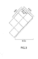
- Fig 3 illustrates how the multiplier of Fig 1 may be extended for use in multiplying together two unsigned eight-bit numbers.
- the extended multiplier seven of the basic 4 x 4 processing cell square arrays are used with three 4 x 4 arrays for processing the carry-over digits.
- the multiplier of Fig 1 only ten of the cells in two of the three 4 x 4 carry-over arrays are used, leaving six cells redundant.
- the pipelined multiplier of Fig 1 may be adapted for use with signed binary numbers where the sign-magnitude representation is used by addition of an EXCLUSIVE-OR gate for processing the sign bits. The magnitude portion of the numbers may then be processed as in Fig 1.
- the multiplier array may be constructed from basic processing cells which are more complex than cell 12.
- a basic cell may readily be constructed, for example, from four of the cells, 12, with internal latches between the cells removed. This cell would then take in two digits of a(n) and two digits of b(n) in one clock cycle.
- the logic for the "macrocell" may be designed particularly for dealing with two bits of both a(n) and b(n) for greater efficiency.
- data words have a number of bits which is divisible by four.
- a macrocell equivalent to a 4 x 4 array of cells, 12, may then be used.
- the numbers a(n) and b(n) are first considered in eight-bit two's complement notation. Any integer in the region -2 7 to 2 7 -1 may be represented uniquely in this way and, in particular, a four-bit two's complement number takes its original four-bit two's complement form with the sign bit extended into the four most significant places. For a(n) positive, its sign bit is zero and therefore four bits are sufficient to represent it in eight-bit two's complement form.
- the product of two four-bit two's complement numbers must be within the range -2 7 to 2 7 -1. Consequently the entire calculation of a(n) x b(n) may be carried out in eight-bit two's complement rotation. For a(n) positive the calculation is effected by multiplying the four-bit two's complement form of a(n) by the eight-bit two's complement form of b(n) and ignoring terms in 2 8 and greater which are generated in the process.
- the result, s(n) is the product a(n) x b(n) in eight-bit two's complement form.
- Fig 4 this is performed in the multiplier shown which includes an array, 100, comprising two sixteen-cell square arrays of processing cells identical to the square array ABCD of Fig 1.
- the digits of a(n) in four-bit two's complement form are input along edge FG of array 100 and the digits of b(n) in eight-bit two's complement form are input along edge FI of the array.
- the digits of a(n), b(n) and s°(n) are input so as to move through the multiplier in a staggered manner.
- the digits b o (n), b 1 (n-1), b 2 (n-2), b 3 ( n - 3 ), b 4 (n-4), b5(n - 5), b 6 ( n-6 ), b 7 (n-7) arrive along edge FI for input simultaneously with the arrival of a 3 ( n ), a 2 ( n- 1), a 1 (n-2) and a o (n-3) along edge FG.
- the multiplier includes an array, 102, consisting of two adjacent sixteen-cell square arrays of identical processing cells, one of which is indicated at 104.
- a cell, 104 is shown in more detail in Fig 6.
- Input lines 14, 16, 18 and 20 bring data into the cell in the form of bits b, s, a and c respectively in a similar manner to the equivalent lines of Fig 2. Also, in a similar manner, output lines 22, 24, 26 and 28 take data away from the cell in the form of bits b', s', c' and a' respectively. Additionally, a fifth line, 106, brings a 'd' control input to the cell, 104, such that
- the d lines of the eight cells 104 adjacent to edge JM are all set to '1' in order to supply the first term of equation "(1)" whilst the remaining cells in the array have blank inputs (equivalent to 0) on their d lines, 106, in order to supply the second term of equation "(1)".
- the value of a3 is input on c 3 line 108 so as to supply the third term of equation "(1)".
- c(n) is set to zero.
- the c 2 (n), c 1 (n) and co(n) latches along edge JK are therefore set to 0.
- Numbers a(n) and b(n) in four-bit and eight-bit two's complement form respectively are then input in a staggered manner along edges JK and JM respectively as shown in the diagram, the result, s(n), being output in staggered manner along edge KL of the array 102.
- the array for the multiplier of Fig 5 is particularly useful compared with prior art multipliers as the correction terms of equation "(1)" are incorporated into the array in one operation without the need for implementing additional operations and processing hardware.
- multiplication of four-bit two's complement numbers a(n) and b(n) is performed using the form ie three correction terms are involved and processed individually.
- the d input is supplied on every cell in Fig 5, it may alternatively be provided only on the cells along the edge JM. However, to retain the iterative nature of the design the input is preferably supplied on all cells.
- Fig 7 depicts an array of processing cells, 110, for performing a one-bit Walsh transform ie a transform of the type
- the processor of Fig 7 is for use with a 4 x 4 matrix W and five-bit two's complement numbers x and y.
- the diagram in Fig 7 illustrates the arrangement of the bits involved in the processing immediately prior to calculation of:
- the elements of W and x(1), x(2), x(3) and x(4) are input to memory sites as shown (x(4) and some of the digits of x(3) and x(2) are not shown in Fi g 7 ).
- Memory sites not containing the elements of x, y or W as shown initially contain blank information (equivalent to digital value 0). These sites are indicated by crosses such as 114 in the upper section of Fig 7 above line NP. For clarity, no crosses are shown in the lower section of Fig 7 below NP.
- Fig 7 The arrangement of Fig 7 is somewhat simplified in that it implies that the w ij are single bit numbers occupying one conducting line each. However, in order to accommodate blank (0) values as well as 1 and -1, the w ij must take a two bit form, (u ij , v ij ).
- the array, 110, of Fig 7 consists of 7 x 5 identical processing cells such as 116 which is shown in more detail in Fig 8.
- the cell, 116 has input lines 118, 119, 120, 122 and 124 for bringing input bits x, u, v, c and y respectively and lines 126, 128, 129, 130 and 132 for outputting bits x', c', v', u' and y' respectively.
- Latches 134, 136, 138, 139 and 140 in the form of memory sites, each for storing a single bit are disposed in lines 132, 118, 119, 120 and 122 respectively.
- a clocking means (not shown) which, in one clock cycle, outputs a first type of clock pulse which causes each memory site to output its stored bit followed by a second type of clock pulse which causes each memory site to store an incoming bit.
- a clocking means not shown
- the W elements and accompanying blanks move vertically downwards by one processing cell repeat distance per clock cycle
- the X elements and adjacent blanks move horizontally to the right by one repeat distance per clock cycle
- the Y elements and adjacent blanks move horizontally to the left by one repeat distance per clock cycle.
- the operation of the processor may be better understood by considering the sequence of events occurring in four of the cells, 116A, 116B, 116C and 116D.
- cell 116B receives 0 inputs on each of its lines 118, 119, 120, 122 and 124.
- cell 116D receives 0 inputs on each of its input lines 118, 119, 120, 122 and 124 and outputs 0 on each of its output lines 126, 128, 129, 130 and 132.
- cell 116B receives:
- cell 116D receives: and and, on the second clock pulse, outputs
- the first digit to be output from the processor is y 0 (1) which emerges at port 142 four clock cycles after the processing begins.
- y 1 (1) then emerges at port 144 after five clock cycles with y 2 (1) reaching port 146 and y 0 (2) reaching port 142 after six clock cycles etc.
- the matrix multiplication is completed when y 4 (4) reaches port 148 sixteen clock cycles after processing begins.
- the numbers, x originally take three-bit, two's complement form, but are extended to five-bit two's complement form for simplicity. This may be appreciated by considering that, in three-bit two's complement form, x, will lie in the range Additionally, for a four-point transform Therefore, the maximum value of y is 12 and the minimum value of Z is -16 y thus lies within the range -2 4 to 2 4- 1 and can therefore be represented in five-bit two's complement form.
- a macrocell array may also be used with the Walsh Transform processor.
- the Fig 7 processor may be adopted for the less complicated matrix multiplication where the w ij take only the values 0 or 1. In this case the w .. would take their conventional one-bit form.
- the processor array may then be considered as a 'bit slice' array and several bit slice arrays may be employed for matrix multiplication where the w.. are multi-bit numbers.
- the Walsh transform processor array of Fig 7 may be employed alongside a stack of other similar processor arrays to cater for multi-bit w ij values.
- the x are made to remain stationary while the Z move one processing cell to the left.
- the y are then made to remain stationary while the x move one processing cell to the right. The result is a reduction in the required number of processing cells.
- an improved processing cell, 160 has input lines 161, 162, 163 and 164 for bringing input bits x, w, c and y respectively and output lines 165, 166, 167 and 168 for outputting bits x', c', w' and y' respectively.
- Latches are also shown associated with cell 160. However, unlike the latches shown in Figs 2, 6, and 8, in Fig 9 each latch is depicted as two half latches. Thus half latches 169, 170, 171, 172, 173, 174, 175 and 176 are disposed in lines 162, 163, 165, 164, 166, 167, 168 and 161 respectively.
- the cell 160 includes a feed back line, 177, in which are disposed two half latches, 178 and 179, and a switch, 180.
- Line 177 carries a digit, y fb , into the cell.
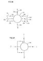
- Fig 10 illustrates a master/slave latch consisting of a master section, 181, and a slave section, 182.
- the latch is controlled by two square wave clocking waveforms, and ⁇ , which are illustrated graphically (voltage vs time) in Fig 11.
- Passage of data bits through the master section, 181, is governed by the pulses and passage of data bits through the slave section, 182, is governed by the ⁇ pulses.
- the latch may be considered as consisting of a separate master half, 181, and a separate slave half, 182.
- latches 169 and 170 are controlled by ⁇ 1
- switch 180 is controlled by ⁇ 2 and such that, on occurrence of a ⁇ 2 peak, the switch closes to connect feed back line 177 to cell 160 and, on occurrence of a ⁇ 2 peak, the switch closes to connect line 164 to the processing cell.
- each x value input to the cell takes part in two processing cell operations before the succeeding x value is input.
- the y input values are likewise updated at half the frequency of the w and c values. However, in their case, the value y is input to the cell for the first of the two operations and the value y fb is input for the second.
- the logic operations of cell 160 may be summed up as: where
- a data processor having a complete array of cells similar to the processing cell of Fig 9 is shown for calculating.
- the data processor has an array, 183, consisting of 4 x 5 processing cells of similar nature to the cell 160 of Fig 9.
- pads, 184 along the upper edge of array 183 for inputting the values of w and along the left-most edge of the array are pads, 185, for inputting the values of x and outputting the values of z.
- An array of latches, 186 is provided between the pads, 185 and the left hand edge of array 183 in order to provide time skew for the input x bits and time deskew for the output y' bits, allowing the x to be input in parallel and the Z to be output in parallel.
- the effect of employing a processing cell as in Fig 9 instead of a processing cell as in Fig 8 is to reduce the 7 x 5 cells (Fig 7) required for a four-point transform to 4 x 5 cells. Consequently, although the Fig 9 cell is more complex than the Fig 8 cell, the final data processor occupies a reduced chip area. In addition, fewer input pads are required in the Fig 13 array than in the Fig 7 array.
- the array of Figure 15 is adapted to carry out the N-point convolution operation: where the a(i) represent a set of positive predetermined coefficient words and the x(n-i) represent a sequence of positive input variables.
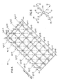
- the array of Figure 15 consists of a square lattice, 200, of 10 x 5 identical prceassing cells, 212, interconnected by conducting lines. The array is shown within the rectangle A'B'C'D'.
- Figure 16 illustrates in detail the operation of a cell, 212.
- a cell, 212 has input lines 214, 216, 218 and 220 for bringing data bits into the cell and output lines 222, 224, 226 and 228 for taking data bits out of the cell. Each line transfers one bit to or from the cell in one cell operation.
- the cell, 212 is a gated full adder which operates such that for bits a, c, s and x input on lines 218, 220, 216 and 214 respectively, and bits a', c', s'and x' output on lines 228, 226, 224 and 222 respectively. and Latches in the form of memory sites 230, 232, 234 and 236, each for storing a single bit, are disposed in lines 216, 220, 218 and 214 respectively.
- each of the cells 212 is governed by a clocking means consisting of two clocks (not shown in the diagram) which output clock pulses such that a first pulse causes each memory site to output its consents into the adjoining line in the directions shown in Figure 16 and a second pulse causes each memory site to store a resulting incoming bit.
- sites 230, 232, 234 and 236 output their contents to processing cell 212 so that the cell operation may be performed on these bits.
- the particular time illustrated in Figure 15 is the time at which the calculation of y(9) and y(10) is taking place.
- cells 212 in array 200 are indicated by square boxes and the interconnecting conducting lines and associated memory sites have been omitted.
- Array 200 consists of ten rows of five cells, 212.
- the value of s input to the first (top) row of cells along edge B'C' is initialised to zero and the value of c input to the fifth (right-most) column of cells along edge C'D' is also made zero.
- the array is therefore arranged to constantly input the value zero to these cells on each clock cycle.
- the bits of x and a which make up a single word are input alternately with zeros and that the x bits may be generally considered to form rightward-leaning parallelograms whilst the bits of a may be generally considered to form leftward-leaning parallelograms.
- the least significant bit of each word enters array 200 first from the left followed two clock cycles later by the next least significant bit etc.
- the most significant bit of each word, a enters array 200 first from the right, followed two clock cycles later by the next most significant bit, etc.
- Region 202 in Figure 15 is associated with the calculation of y(9) and region 204 is associated with the calculation of y(10).
- the cell of Figure 17 is a full adder, 238, having inputs c and s, the value of s being the same as the value of s' output from a vertically neighbouring cell, 212, adjacent to edge A'D'.
- Cell 238 outputs its own partial product, s', and a carry bit, c', this value of s' then being fed back to the input of the cell to be used in the subsequent full adder operation.
- Figure 15 shows that the bits of x and a pass along the rows of processing cells in array 200 cyclically.
- a 2 (2) has emerged from the eighth row along edge A'B' of array 200 following processing by cell numbered 212b in Figure 15,it must on the next clock cycle be input across edge C'D' to cell numbered 212c of the eighth row in Figure 15.
- a result, y accumulates along edge A'D' every seven clock cycles.
- a result, y is accumulated every 2t-1 clock cycles.
- the example of Figure 15 is a simplification of a real convolution processor.
- the maximum width of y would be more than 2t-1 bits.
- extra half adder cells are required along edge A'B' in order to deal with the maximum word width of the accumulating product, y, in any particular row.
- the number of full adder cells, 238, provided along edge A'D' must also be increased.
- the words x and a may be extended to a width equal to the maximum width of y. In the example of Figure 1 5 ,the number of cells in array 200 would be increased accordingly.
- the processor of Figure 15 may be adapted to deal with non-positive x and a by expressing both the variables, x. and the coefficient words, a, in two's complement form and extending their word widths to the maximum width of any y before inputting them to the array.
- a processor as illustrated in Figurel8 may then be used to perform the convolution operation.
- Figure 18 illustrates the example of a ten point convolution equivalent to that of equation '(2)' above where the maximum width of y is taken to be three bits.
- the x and a are therefore expressed in three bit , two's complement form. Since the maximum width of y is three bits, any bits of four or more may be ignored.
- the result is an array, 300, of 10 x 3 processing cells, 212, each identical to cell 212 of Figure 16. Regions within array 300 which produce non-zero results are indicated by triangular regions 302 and 304. At the instant shown in Figure 18,region 302 is involved in calculation of y(9) and region 304 is involved in calculation of y(10).
- an alternative method of accommodating the full width of any y is by providing extra cells to the left of array 300 according to the maximum width of y in any row of the array.
- the bits of x and a move cyclically through the processing cells of array 300 of Figure 18.
- edges of array 300 to be defined by A"B"C"D" and the width of words x and a to be l bits
- a bit of a coefficient word a which emerges from the array along A"B" is again input to the same row across edge C"D" l-1 clock cycles later.
- a bit of a variable x which emerges from the array across C"D" is again input across edge A"B" to the next higher row l-2 clock cycles later.
- the bits of a word a therefore move cyclically within a particular row whilst the bits of the words x spiral up the array.
- the necessary delays of l-1 and l-2 clock cycles may be provided by clocking the bits of a and x respectively back through l-1 and l-2 latches before again introducing them into the array. From this it can be seen that, although ten input pins are required along C"D" to input the bits of coefficient words a, only one input pin is required at the bottom of A"B" to input all bits of every x.
- the processor of Figure 18 may be modified for use in adaptive filtering by allowing for the input pins along C"D" to be disabled at an appropriate time to input new values of a.
- a truncated array is illustrated in Figure 1 9.
- the array, 400, of cells is for a five point convolution in which the a and x words take two's complement form and are sign extended to four bits wide which is the full range of the result.
- the results, y, have been truncated by removing the right hand-most column of cells.
- the l ' clock cycle delays are thus provided by adding an extra latch, 402, to each processing cell, 412, and the l ' + 1 clock cycle delays are provided by adding an extra latch, 404, to each cell in addition to a supplemental latch, 406, at the right hand side of each row of cells.
- the bits of x and a are then clocked back through these latches after leaving the array before re-entering again.
- FIG. 20 shows the processing cell, 412, of Figure 19 in more detail.
- the array of Figure 19 is also accompanied by a row of full adder cells, 238, identical to the cell of Figure 17 for accumulating the results, y, at the bottom of the array.
- Fig 24 depicts in a very simplified form an instantaneous picture of the interaction of variables, x with coefficients a in part of a convolution operation similar to that illustrated in Fig 15. For simplicity only those cells at which the a and x do not take a zero value are shown in Fig 24.
- bits of coefficient words a which lie on line 600 of Fig 24 are least significant bits of the a
- the bits on line 602 are next least significant bits and the bits on line 604 are most significant bits.
- the bits of the x which lie on line 606 are least significant bits
- the bits on line 608 are next least significant bits and the bits on line 610 are most significant bits.
- x and a take the form of three-bit two's complement numbers it can be seen that at the processing cells shown shaded in Fig 24 a sign (most significant) bit meets a non-sign bit whilst at the remaining cells either a sign bit meets a sign bit or a non-sign bit meets a non-sign bit.
- the processing cell array can be split into two regions having different types of cells. These regions are illustrated as regions A and B in Fig 25. For a proaessing c ⁇ ll array as illustrated in Fig 25 to be able to perform a convolution operation, the shaded cells in region A must be able to distinguish between:
- FIG. 6 A processing cell, 612, suitable for inclusion in region A is illustrated in Fig 26.
- the d input to the top cell of the column is conveniently perpetually set to 0 as there are . no shaded cells in this column.
- the d input is conveniently set to 1 at all times.
- the d input is conveniently set to 1 according to the following format:
- processing cells of region B of Fig 25 are made up of cells equivalent to cell 212 of Fig 16.
- extra half adder cells for accommodating word growth of y may be included to the left of region A and truncation of the B region is possible if the least significant bits of y are not required.
- the above ideas are not confined to the convolution operation.
- the convolution arrays may, for example, be straightforwardly adapted to perform a correlation operation ie to perform the calculation:
- the correlation array is the same as that of Figure 17 except that a(0) is input to the first (top-most) row, a(1) to the second row etc instead of a(0) being input to the tenth (bottom-most) row, a(1) to the ninth row etc as in the convolution array of Figure 18.
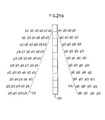
- an array, 500 is indicated schematically by a column of boxes. Each box represents a row of processing cells equivalent to a row of cells in Figure 18.
- the arrangement of variables, x, and coefficient words, a, needed for the correlation operation to take place is indicated at 502 and 504 respectively.
- each x and each a is input in a bit serial fashion with zeros separating the bits of each word, but with no zeros separating the bits of successive words. It will also be appreciated that the repetition of values of x and a is effected by recycling these words as in the Figure 18 embodiment.
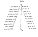
- Figure 21(b) illustrates the equivalent word level diagram for the convolution processor of Figure 18.
- Figure 22 illustrates at word level in a similar manner to Figure 21the arrangement of multi-bit variables, x, and coefficient words a for carrying out the matrix-vector multiplication.
- Figure 23 depicts in a similar manner to Figure 22 the word level arrangement of variables. x, and coefficient words, a, for carrying out the banded matrix-vector multiplication.
- truncation by one bit was illustrated. In general, however, truncation by more than one bit may be adopted provided that a corresponding correction term is added to the resulting L and provided that delay latches are included in order to preserve the integrity of the timing.
- the invention aslows the fabrication of frocessors with regular, repetitive designs.
- the design problem is restricted to the design of a single processing cell. Having proven a single cell, the whole array of identical cells is ince the array consists merely of single cells connected to immediate neighbouring cells.
- the iterative property of the design is advantageous in allowing processors able to deal with more bits per number to be made.
- the processors are enlarged merely by adding more processing cells to the array and this can be done without cost to the speed of operation of the processors.
- this may be expanded to allow multiplication of a(n) (l bits per word) by b(n) (m bits per word) by providing a rectangular array of l x m processing cells adjoined to a triangular array of % (l+1) cells.
- data words have a number of bits which is divisible by four, thus allowing the sixteen cell square array to become a unit array which may be -used as a basic building block.
- the larger building block may be constructed with all internal latches removed so as to effectively form a new unit processing cell.
- additional circuits are incorporated to allow correction terms to be processed therefore preventing simple adjoining of basic modules without reprogramming for fabrication of a larger multiplier.
- the latency of the inventive processors ie the nett number of clock cycles required between input of data and output of a complete answer
- this disadvantage is offset by the fact that the pipelining allows input of a data word at each clock cycle or at every second clock cycle according to the type of processor.
- the final clock rate is a function of the delay in processing one batch of data bits in a processing cell only and the maximum rate attainable is equal to the processing cell delay.
- the inventive design allows this delay to be made very small.
- the inventive processor design promotes high frequency processing since, in one clock cycle, data is passed only as far as the nearest latch - a distance which can be made very small, particularly in VLSI. Transmission of data over long connecting lines and resulting time delays, especially the long delays resulting when transmission line effects come into play, are, therefore, avoided. The associated problems of introducing stray capacitance when using extensive data transmission lines are also avoided thereby eliminating the need for large drivers to broadcast the data across the chip. Equally alleviated are the difficulties concerning power dissipation of large drivers and the drivers themselves both taking up large amounts of chip area and introducing further driver chain time delays. In the inventive design the necessary driving is effectively incorporated into the latching circuits, thereby giving a distributed power consumption.
- synchronisation of timing is readily achieved as the processing cells are of simple design and data is transmitted to neighbouring cells only. Additionally, propagation delays are made independent of data word size unlike, for example, prior art pipelined and ripple-through processors in which one processing step includes the broadcasting of a bit of b(n) to each bit of a(n) before the processing step is complete.
- a further advantage of the inventive design is that, by avoiding driving problems, the size of the processor is not limited by data word size.
- a still further advantage of the inventive design is the economy in chip area used as a result of interconnections running between immediately neighbouring processing cells only.
- control of the inventive processor is additionally relatively simple since very few types of clock signals are required for controlling the latches.
- the inventive processor may be considered as consisting of successive pipeline stages.
- the timing constraints for the inventive processor are therefore,firstly, that the timing line path lengths should be arranged so that pulses within any given stage are synchronised, and, secondly, that the delays between adjacent stages are such that, when a first stage is outputting bits to a neighbouring stage, the neighbouring stage comes under the influence of a timing pulse controlling storage of data and not a timing pulse which controls output of data. If the neighbouring stage were under the influence of a timing pulse controlling output of data, the data would pass through the neighbouring stage without being latched into the memory sites. Complete synchronisation between stages is therefore not necessary, a degree of delay being tolerable.
- multiplexing of data words may be employed so as to economise on the number of input and output pins required in a single chip processor although this may decrease the overall speed of the processor.
- a further modification of the inventive design involves inclusion of a degree of fault tolerance.
- the regularity of the design makes this particularly simple. For example, if a particular processing cell is found to be malfunctioning, the row and column containing the cell may be made redundant and a means of by-passing cells incorporated into the cell design so as to avoid use of the cells on the row and column.
- the by-pass connections may be activated using, for example, a form of matrix address control or may be activated using burning of on-chip links by means of, for instance, current pulse or laser techniques.
- a chip incorporating the inventive design may take the form of an uncommitted cell array, the necessary circuit connections for the required array being formed in a subsequent metallisation process.
- the invention is particularly suited to this type of design since many applications require similar cells. The possible variations are therefore readily accommodated on the chip for later wiring. Additionally, due to the regularity of the architecture, laying of subsequent metallisations is relatively uncomplicated.
- the inventive design may operate at a sufficiently high frequency to enable use of dynamic latches and, therefore, be particularly suited for the use of MOS technology.
- dynamic By using dynamic in contrast to the more bulky static latches, a minimum of chip area is therefore occupied by latches.
- the increased design problems associated with MOS eg the need for good impedance matching and good synchronisation in opening and closing of transmission gates so as to prevent back-flow of charge
- the concomitant complex testing and simulation of the circuits required during design are alleviated as a result of the regularity of the architecture.
- the additional difficulty arising from the need to minimise stray capacity in order to minimise required driving power is also alleviated due to the minimum of interconnecting lines in the inventive design.
Landscapes
- Engineering & Computer Science (AREA)
- Physics & Mathematics (AREA)
- General Physics & Mathematics (AREA)
- Theoretical Computer Science (AREA)
- Computational Mathematics (AREA)
- Mathematical Analysis (AREA)
- Mathematical Optimization (AREA)
- Pure & Applied Mathematics (AREA)
- General Engineering & Computer Science (AREA)
- Mathematical Physics (AREA)
- Computing Systems (AREA)
- Data Mining & Analysis (AREA)
- Algebra (AREA)
- Databases & Information Systems (AREA)
- Software Systems (AREA)
- Computer Hardware Design (AREA)
- Complex Calculations (AREA)
Applications Claiming Priority (4)
| Application Number | Priority Date | Filing Date | Title |
|---|---|---|---|
| GB8125222 | 1981-08-18 | ||
| GB8125222 | 1981-08-18 | ||
| GB8211416 | 1982-04-20 | ||
| GB8211416 | 1982-04-20 |
Publications (3)
| Publication Number | Publication Date |
|---|---|
| EP0073116A2 true EP0073116A2 (fr) | 1983-03-02 |
| EP0073116A3 EP0073116A3 (en) | 1985-01-09 |
| EP0073116B1 EP0073116B1 (fr) | 1988-12-14 |
Family
ID=26280504
Family Applications (1)
| Application Number | Title | Priority Date | Filing Date |
|---|---|---|---|
| EP19820304165 Expired EP0073116B1 (fr) | 1981-08-18 | 1982-08-06 | Circuits intégrés de traitement de données |
Country Status (4)
| Country | Link |
|---|---|
| EP (1) | EP0073116B1 (fr) |
| CA (1) | CA1196422A (fr) |
| DE (1) | DE3279288D1 (fr) |
| GB (1) | GB2106287B (fr) |
Cited By (3)
| Publication number | Priority date | Publication date | Assignee | Title |
|---|---|---|---|---|
| EP0144123A3 (en) * | 1983-10-05 | 1986-03-19 | National Research Development Corporation | Digital data processor for multiplying data elements by coefficients |
| EP0186958A3 (en) * | 1984-12-18 | 1988-01-07 | National Research Development Corporation | Digital data processor for matrix-vector multiplication digital data processor for matrix-vector multiplication |
| WO1988007722A3 (fr) * | 1987-03-28 | 1988-10-20 | Stonefield Systems Plc | Ameliorations apportees a des processeurs vectoriels cellulaires |
Families Citing this family (3)
| Publication number | Priority date | Publication date | Assignee | Title |
|---|---|---|---|---|
| IT1182575B (it) * | 1985-09-27 | 1987-10-05 | Elsag | Sistema per realizzare elaborazioni convolutive veloci su informazioni rappresentative di immagini |
| US4769779A (en) * | 1985-12-16 | 1988-09-06 | Texas Instruments Incorporated | Systolic complex multiplier |
| GB2187579B (en) * | 1986-03-05 | 1989-11-15 | Secr Defence | Digital processor for convolution and correlation |
-
1982
- 1982-08-06 GB GB08222685A patent/GB2106287B/en not_active Expired
- 1982-08-06 DE DE8282304165T patent/DE3279288D1/de not_active Expired
- 1982-08-06 EP EP19820304165 patent/EP0073116B1/fr not_active Expired
- 1982-08-09 CA CA000409023A patent/CA1196422A/fr not_active Expired
Non-Patent Citations (7)
| Title |
|---|
| AUTOMATISME, vol. 21, no. 10, October 1976, pages 302-314, Paris, FR; M. MRAYATI et al.: "Conception et réalisation de filtres numériques" * |
| ELECTRONICS LETTERS, vol. 18, no. 6, March 1982, pages 241-243, London, GB; J.V. McCANNY et al.: "Implementation of signal processing functions using 1-bit systolic arrays" * |
| ELECTRONICS LETTERS, vol. 8, no. 4, 24th February 1972, pages 100-101, Hitchin, Herts, GB; K.J. DEAN et al.: "General iterative array" * |
| IEEE TRANSACTIONS ON COMPUTERS, vol. 21, no. 8, August 1972, pages 880-886, IEEE, New York, US; T.G. HALLIN et al.: "Pipelining of arithmetic functions" * |
| IEEE TRANSACTIONS ON COMPUTERS, vol. C-24, no. 3, March 1975, pages 317-322, New York, US; J. DEVERELL: "Pipeline iterative arithmetic arrays" * |
| SIGNAL PROCESSING: THEORIES AND APPLICATIONS, PROCEEDINGS OF EUSIPCO-80, FIRST EUROPEAN SIGNAL PROCESSING CONFERENCE, 16th-18th September 1980, Lausanne, CH, North-Holland Publishing Company, Amsterdam, NL; L. CIMINIERA et al.: "High speed correlator circuits" * |
| THE RADIO AND ELECTRONIC ENGINEER, vol. 45, no. 3, March 1975, pages 116-120, London, GB; P.M. THOMPSON et al.: "Digital arithmetic units for a high data rate" * |
Cited By (3)
| Publication number | Priority date | Publication date | Assignee | Title |
|---|---|---|---|---|
| EP0144123A3 (en) * | 1983-10-05 | 1986-03-19 | National Research Development Corporation | Digital data processor for multiplying data elements by coefficients |
| EP0186958A3 (en) * | 1984-12-18 | 1988-01-07 | National Research Development Corporation | Digital data processor for matrix-vector multiplication digital data processor for matrix-vector multiplication |
| WO1988007722A3 (fr) * | 1987-03-28 | 1988-10-20 | Stonefield Systems Plc | Ameliorations apportees a des processeurs vectoriels cellulaires |
Also Published As
| Publication number | Publication date |
|---|---|
| GB2106287A (en) | 1983-04-07 |
| GB2106287B (en) | 1986-01-02 |
| EP0073116B1 (fr) | 1988-12-14 |
| CA1196422A (fr) | 1985-11-05 |
| DE3279288D1 (en) | 1989-01-19 |
| EP0073116A3 (en) | 1985-01-09 |
Similar Documents
| Publication | Publication Date | Title |
|---|---|---|
| US4639857A (en) | Digital data processor incorporating an orthogonally connected logic cell array | |
| EP0186958B1 (fr) | Processeur de données numériques pour la multiplication de matrices et de vecteurs | |
| Thompson | Fourier Transforms in VLSI. | |
| Kung et al. | A Systolic 2-D Convolution Chip. | |
| US4736335A (en) | Multiplier-accumulator circuit using latched sums and carries | |
| US4489393A (en) | Monolithic discrete-time digital convolution circuit | |
| KR20010040263A (ko) | 고속의 정규 곱셈기 구조 | |
| EP0152046A2 (fr) | Circuit de multiplication | |
| EP0113391B1 (fr) | Multiplicateur numérique et méthode d'addition des produits partiels dans un multiplicateur numérique | |
| US4686645A (en) | Pipelined systolic array for matrix-matrix multiplication | |
| EP0471723B1 (fr) | Processeur numerique pour calculs de complements a deux | |
| Ngai et al. | Regular, area-time efficient carry-lookahead adders | |
| EP0237204B1 (fr) | Processeur numérique structuré en tranches de bits pour corrélation et convolution | |
| US4796219A (en) | Serial two's complement multiplier | |
| Odugu et al. | Implementation of low power and memory efficient 2D FIR filter architecture | |
| EP0073116B1 (fr) | Circuits intégrés de traitement de données | |
| US5047974A (en) | Cell based adder with tree structured carry, inverting logic and balanced loading | |
| KR100245944B1 (ko) | 승산장치 | |
| Smith et al. | Radix-4 modules for high-performance bit-serial computation | |
| US5072419A (en) | Binary tree multiplier constructed of carry save adders having an area efficient floor plan | |
| Thamizharasan et al. | Proficient architecture for vedic multiplier using various VLSI design techniques of optimized adder | |
| Ramamoorthy et al. | Fast multiplication cellular arrays for LSI implementation | |
| EP0174397A2 (fr) | Circuit logique comprenant une seule horloge pour logique à niveaux multiples, commandé par une charge fictive | |
| DADDAC | Some schemes for parallel multipliers | |
| US20260045296A1 (en) | Compact in-memory computer architecture |
Legal Events
| Date | Code | Title | Description |
|---|---|---|---|
| PUAI | Public reference made under article 153(3) epc to a published international application that has entered the european phase |
Free format text: ORIGINAL CODE: 0009012 |
|
| AK | Designated contracting states |
Designated state(s): DE FR NL |
|
| 17P | Request for examination filed |
Effective date: 19830805 |
|
| PUAL | Search report despatched |
Free format text: ORIGINAL CODE: 0009013 |
|
| AK | Designated contracting states |
Designated state(s): DE FR NL |
|
| 17Q | First examination report despatched |
Effective date: 19861217 |
|
| R17C | First examination report despatched (corrected) |
Effective date: 19870629 |
|
| GRAA | (expected) grant |
Free format text: ORIGINAL CODE: 0009210 |
|
| AK | Designated contracting states |
Kind code of ref document: B1 Designated state(s): DE FR NL |
|
| REF | Corresponds to: |
Ref document number: 3279288 Country of ref document: DE Date of ref document: 19890119 |
|
| ET | Fr: translation filed | ||
| PLBE | No opposition filed within time limit |
Free format text: ORIGINAL CODE: 0009261 |
|
| STAA | Information on the status of an ep patent application or granted ep patent |
Free format text: STATUS: NO OPPOSITION FILED WITHIN TIME LIMIT |
|
| 26N | No opposition filed | ||
| NLS | Nl: assignments of ep-patents |
Owner name: THE SECRETARY OF STATE FOR DEFENCE IN HER BRITANNI |
|
| REG | Reference to a national code |
Ref country code: FR Ref legal event code: TP |
|
| PGFP | Annual fee paid to national office [announced via postgrant information from national office to epo] |
Ref country code: FR Payment date: 20010705 Year of fee payment: 20 |
|
| PGFP | Annual fee paid to national office [announced via postgrant information from national office to epo] |
Ref country code: DE Payment date: 20010718 Year of fee payment: 20 |
|
| PGFP | Annual fee paid to national office [announced via postgrant information from national office to epo] |
Ref country code: NL Payment date: 20010719 Year of fee payment: 20 |
|
| REG | Reference to a national code |
Ref country code: FR Ref legal event code: TP |
|
| PG25 | Lapsed in a contracting state [announced via postgrant information from national office to epo] |
Ref country code: NL Free format text: LAPSE BECAUSE OF EXPIRATION OF PROTECTION Effective date: 20020806 |
|
| NLS | Nl: assignments of ep-patents |
Owner name: QINETIQ LIMITED |
|
| NLV7 | Nl: ceased due to reaching the maximum lifetime of a patent |
Effective date: 20020806 |