EP0073721A2 - Dispositif à semi-conducteur intégré à grand échelle comprenant un détecteur de défauts et son procédé de fabrication - Google Patents
Dispositif à semi-conducteur intégré à grand échelle comprenant un détecteur de défauts et son procédé de fabrication Download PDFInfo
- Publication number
- EP0073721A2 EP0073721A2 EP82401588A EP82401588A EP0073721A2 EP 0073721 A2 EP0073721 A2 EP 0073721A2 EP 82401588 A EP82401588 A EP 82401588A EP 82401588 A EP82401588 A EP 82401588A EP 0073721 A2 EP0073721 A2 EP 0073721A2
- Authority
- EP
- European Patent Office
- Prior art keywords
- wiring
- semiconductor device
- monitor
- lsi
- chips
- Prior art date
- Legal status (The legal status is an assumption and is not a legal conclusion. Google has not performed a legal analysis and makes no representation as to the accuracy of the status listed.)
- Granted
Links
Images


Classifications
-
- H—ELECTRICITY
- H10—SEMICONDUCTOR DEVICES; ELECTRIC SOLID-STATE DEVICES NOT OTHERWISE PROVIDED FOR
- H10P—GENERIC PROCESSES OR APPARATUS FOR THE MANUFACTURE OR TREATMENT OF DEVICES COVERED BY CLASS H10
- H10P74/00—Testing or measuring during manufacture or treatment of wafers, substrates or devices
- H10P74/27—Structural arrangements therefor
- H10P74/277—Circuits for electrically characterising or monitoring manufacturing processes, e.g. circuits in tested chips or circuits in testing wafers
-
- H—ELECTRICITY
- H10—SEMICONDUCTOR DEVICES; ELECTRIC SOLID-STATE DEVICES NOT OTHERWISE PROVIDED FOR
- H10W—GENERIC PACKAGES, INTERCONNECTIONS, CONNECTORS OR OTHER CONSTRUCTIONAL DETAILS OF DEVICES COVERED BY CLASS H10
- H10W20/00—Interconnections in chips, wafers or substrates
- H10W20/40—Interconnections external to wafers or substrates, e.g. back-end-of-line [BEOL] metallisations or vias connecting to gate electrodes
Definitions
- the present invention relates to a large-scale integration semiconductor device wherein a monitor element for monitoring the wiring formation condition is formed on the product chip of the semiconductor device.
- monitor chips are formed on appropriate positions of a wafer at the same time as the LSI product chips, as shown in Fig. 1.
- Figure 1 shows a semiconductor wafer 11 from which a large number of LSI chips 12 including monitor chips 13 are produced in matrix fashion.
- One of the monitor chips 13 has a circuit for monitoring the formation of active elements such as diodes and transistors.
- the monitor chip 13 is used for inspecting for faults arising from the manufacturing process of the LSI chips.
- LSI chips have been designed both for greater integration scale and increased dimensions. This has meant fewer product chips obtained from one piece of wafer. Under such conditions, it is not desirable to form monitor chips on wafers, each monitor chip would mean one less product chip.
- monitor chips on the wafer increases the time necessary for manufacturing LSI chips, especially when using the direct-step-and-repeat-method exposing process.
- Such LSI chips of increased integration scale have a greater area of metal wirings connecting the bulks than the area of active bulks in the chip.
- Recent developments in LSI manufacturing technology have also significantly reduced the possibility of faults in the active bulk area.
- the main factor behind faults in the product chips has become the formation of the multi--layer metal wirings. Faults in the active bulk area can now be neglected.-- Use of monitor chips to check only the wiring formation in product chips would be inefficient.
- the object of the present invention is to solve the above-mentioned problems in increased-integration-scale LSI semiconductor devices and to provide an LSI semiconductor device having a monitor element; formed in the unused area of the chip, for checking the wiring formation, thereby eliminating the need for monitor chips.
- an LSI semiconductor device having a monitor element.
- the monitor element comprises a wiring pattern for monitoring the wiring formation on the semiconductor substrate, and monitor terminal portions formed at both ends of said wiring pattern.
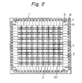
- Figure 2 shows a plan view of the LSI semiconductor device.
- the LSI semiconductor device may be manufactured by using a master-slice method.
- a plurality of basic cells BC are arranged in matrix fashion in a basic cell array 2.
- the basic cell array 2 is formed on the center of an LSI chip 1.
- Input/output buffers 3 are formed along the sides of the LSI chip 1.
- Signal pads 4 for input/ output buffers 3 are arranged in rows along the sides of the LSI chip 1.
- pads 5 and 6 for the ground GND and for the voltage source V cc are formed.
- the areas around the pads 5 and 6 are not used in the semiconductor device.
- a monitor element 7 and a monitor pad 8 are formed in one corner of the LSI chip 1.
- the monitor element 7 of Fig. 2 is illustrated in more detail in Fig. 3.
- Figure 3 shows an enlarged view of a corner of the LSI 1.
- the monitor element 7 is formed above a depression 9 formed in the unused area of the LSI chip 1.
- the monitor element 7 has a wiring pattern 71 and monitor terminal portions 72.
- the wiring pattern 71 has a wiring portion, and the wiring portion is formed in the same process step of forming a wiring layer for interconnecting the active elements such as diodes and transistors.
- the wiring pattern 71 of the monitor element 7 is formed along the step portion of the depression 9 in such a way that the wiring line of the wiring pattern 71 runs back and forth across the step of the depression 9.
- the ends of the wiring pattern 71 are connected to the pad for the voltage source 6 and the monitor pad 8 through the monitor terminal portions 72.
- FIG. 4A and 4B A principal portion of the wiring pattern 71 of the monitor element 7 is illustrated in Figs. 4A and 4B.
- Figure 4B is a sectional view of the above-mentioned portion along the line B-B.
- SB indicates a semiconductor substrate
- OF indicates an oxidation film of polysilicon or phosphosilicate glass (PSG)
- MW indicates a metal wiring layer.
- the structure of the metal wiring layer MW of Fig. 4B is used for monitoring the wiring formation of the LSI chip, i.e., to determine whether any faults have occurred in the wiring lines in the manufacturing process.
- FIG. 4C shows the sectional view of the wiring pattern 71 in which the disconnection of the metal wiring layer MW is produced by poor positioning or etching in the manufacturing process.
- the above-mentioned fault of the wiring layer can be detected by using the pad for voltage source 6 and the monitor pad 8 (Fig. 3).
- the line width of the wiring pattern 71 of the monitor element may be designed to be equal to the minimum line width of the wiring lines used for forming the semiconductor device in order to monitor the worst condition for the wiring formation.
- the wiring pattern 71 of the monitor element 7 according to the present invention may have a through hole portion as shown in Figs. 5A and 5B.
- Fig. 5A two wiring patterns 71' and 71" are connected to each other via a through hole.
- the wiring formation in an LSI chip can be monitored without using monitor chips. Therefore, the effective number of product chips produced from one wafer can be increased. Further, since it is not necessary to form two types of chips (product chips and monitor chips) on the same wafer, the efficiency of manufacture of the LSI chips can be increased, even when the direct-step-and-repeat-method exposing process is used. Still further, since the monitor elements are formed in the unused area (dead area) of the LSI chips, the overall area of the LSI chips can be used more efficiently.
Landscapes
- Semiconductor Integrated Circuits (AREA)
- Testing Or Measuring Of Semiconductors Or The Like (AREA)
- Design And Manufacture Of Integrated Circuits (AREA)
Applications Claiming Priority (2)
| Application Number | Priority Date | Filing Date | Title |
|---|---|---|---|
| JP135211/81 | 1981-08-28 | ||
| JP56135211A JPS602775B2 (ja) | 1981-08-28 | 1981-08-28 | モニタ機能付大規模集積回路及びその製造方法 |
Publications (3)
| Publication Number | Publication Date |
|---|---|
| EP0073721A2 true EP0073721A2 (fr) | 1983-03-09 |
| EP0073721A3 EP0073721A3 (en) | 1984-07-18 |
| EP0073721B1 EP0073721B1 (fr) | 1987-10-28 |
Family
ID=15146439
Family Applications (1)
| Application Number | Title | Priority Date | Filing Date |
|---|---|---|---|
| EP82401588A Expired EP0073721B1 (fr) | 1981-08-28 | 1982-08-26 | Dispositif à semi-conducteur intégré à grand échelle comprenant un détecteur de défauts et son procédé de fabrication |
Country Status (4)
| Country | Link |
|---|---|
| EP (1) | EP0073721B1 (fr) |
| JP (1) | JPS602775B2 (fr) |
| DE (1) | DE3277560D1 (fr) |
| IE (1) | IE53794B1 (fr) |
Cited By (5)
| Publication number | Priority date | Publication date | Assignee | Title |
|---|---|---|---|---|
| WO1988002182A1 (fr) * | 1986-09-17 | 1988-03-24 | The General Electric Company, P.L.C. | Procede de fabrication de circuits integres |
| WO1988002123A1 (fr) * | 1986-09-17 | 1988-03-24 | The General Electric Company, P.L.C. | Circuits integres |
| EP0374466A1 (fr) * | 1988-12-22 | 1990-06-27 | International Business Machines Corporation | Moniteurs pour procédé d'interconnexions en couches minces |
| EP0533269A3 (en) * | 1991-09-19 | 1994-05-18 | Ibm | Test structure for multi-layer, thin-film modules |
| EP0610922A3 (fr) * | 1993-02-12 | 1998-01-21 | Nec Corporation | Dispositif de mémoire à semi-conducteur |
Families Citing this family (3)
| Publication number | Priority date | Publication date | Assignee | Title |
|---|---|---|---|---|
| JP2590553B2 (ja) * | 1987-12-07 | 1997-03-12 | 日本電気株式会社 | 半導体装置 |
| CH684644A5 (de) | 1992-07-13 | 1994-11-15 | Eprova Ag | 5,10-Methylentetrahydrofolsäure-Cyclodextrin-Einschlussverbindungen. |
| US7240322B2 (en) * | 2005-04-04 | 2007-07-03 | International Business Machines Corporation | Method of adding fabrication monitors to integrated circuit chips |
Family Cites Families (1)
| Publication number | Priority date | Publication date | Assignee | Title |
|---|---|---|---|---|
| US4243937A (en) * | 1979-04-06 | 1981-01-06 | General Instrument Corporation | Microelectronic device and method for testing same |
-
1981
- 1981-08-28 JP JP56135211A patent/JPS602775B2/ja not_active Expired
-
1982
- 1982-08-26 EP EP82401588A patent/EP0073721B1/fr not_active Expired
- 1982-08-26 DE DE8282401588T patent/DE3277560D1/de not_active Expired
- 1982-08-30 IE IE2103/82A patent/IE53794B1/en not_active IP Right Cessation
Cited By (5)
| Publication number | Priority date | Publication date | Assignee | Title |
|---|---|---|---|---|
| WO1988002182A1 (fr) * | 1986-09-17 | 1988-03-24 | The General Electric Company, P.L.C. | Procede de fabrication de circuits integres |
| WO1988002123A1 (fr) * | 1986-09-17 | 1988-03-24 | The General Electric Company, P.L.C. | Circuits integres |
| EP0374466A1 (fr) * | 1988-12-22 | 1990-06-27 | International Business Machines Corporation | Moniteurs pour procédé d'interconnexions en couches minces |
| EP0533269A3 (en) * | 1991-09-19 | 1994-05-18 | Ibm | Test structure for multi-layer, thin-film modules |
| EP0610922A3 (fr) * | 1993-02-12 | 1998-01-21 | Nec Corporation | Dispositif de mémoire à semi-conducteur |
Also Published As
| Publication number | Publication date |
|---|---|
| JPS602775B2 (ja) | 1985-01-23 |
| EP0073721B1 (fr) | 1987-10-28 |
| IE822103L (en) | 1983-02-28 |
| IE53794B1 (en) | 1989-02-15 |
| DE3277560D1 (en) | 1987-12-03 |
| EP0073721A3 (en) | 1984-07-18 |
| JPS5848933A (ja) | 1983-03-23 |
Similar Documents
| Publication | Publication Date | Title |
|---|---|---|
| KR100294771B1 (ko) | 반도체장치 | |
| EP0494782B1 (fr) | Système de test et de vieillissement thermique pour une plaquette semi-conductrice et méthode pour sa fabrication | |
| EP0073149B1 (fr) | Module de montage pour puce semi-conductrice | |
| US6121677A (en) | Reduced size integrated circuits and methods using test pads located in scribe regions of integrated circuits wafers | |
| US5262719A (en) | Test structure for multi-layer, thin-film modules | |
| US6031257A (en) | Semiconductor integrated circuit device | |
| EP0109006B1 (fr) | Mémoire dynamique à accès aléatoire à voies d'accès de tension séparées, pour "brûlage" et méthodes de fabrication et de test d'une telle mémoire | |
| JPH0577184B2 (fr) | ||
| KR0142570B1 (ko) | 반도체 집적회로 장치 및 그 제조방법 | |
| US11901338B2 (en) | Interwafer connection structure for coupling wafers in a wafer stack | |
| JPH07111971B2 (ja) | 集積回路装置の製造方法 | |
| US20050139987A1 (en) | Semiconductor integrated circuit device | |
| EP0073721A2 (fr) | Dispositif à semi-conducteur intégré à grand échelle comprenant un détecteur de défauts et son procédé de fabrication | |
| US7105933B2 (en) | Semiconductor integrated circuit device and manufacturing method of the same | |
| JP2874682B2 (ja) | 半導体装置 | |
| US7238962B2 (en) | Semiconductor chip with test pads and tape carrier package using the same | |
| US4717988A (en) | Universal wafer scale assembly | |
| US6479306B1 (en) | Method for manufacturing semiconductor device | |
| US4942447A (en) | Borderless master slice CMOS device | |
| TW202501772A (zh) | 非對稱接墊結構及其應用 | |
| US20030227080A1 (en) | Multi-chip module | |
| JPH11330256A (ja) | 半導体装置およびその製造方法 | |
| JPH0542823B2 (fr) | ||
| KR100541798B1 (ko) | 반도체 장치의 테그 패턴 형성방법 | |
| CN219350223U (zh) | 芯片电路结构 |
Legal Events
| Date | Code | Title | Description |
|---|---|---|---|
| PUAI | Public reference made under article 153(3) epc to a published international application that has entered the european phase |
Free format text: ORIGINAL CODE: 0009012 |
|
| AK | Designated contracting states |
Designated state(s): DE FR GB |
|
| PUAL | Search report despatched |
Free format text: ORIGINAL CODE: 0009013 |
|
| AK | Designated contracting states |
Designated state(s): DE FR GB |
|
| 17P | Request for examination filed |
Effective date: 19841220 |
|
| 17Q | First examination report despatched |
Effective date: 19860225 |
|
| GRAA | (expected) grant |
Free format text: ORIGINAL CODE: 0009210 |
|
| AK | Designated contracting states |
Kind code of ref document: B1 Designated state(s): DE FR GB |
|
| REF | Corresponds to: |
Ref document number: 3277560 Country of ref document: DE Date of ref document: 19871203 |
|
| ET | Fr: translation filed | ||
| PLBE | No opposition filed within time limit |
Free format text: ORIGINAL CODE: 0009261 |
|
| STAA | Information on the status of an ep patent application or granted ep patent |
Free format text: STATUS: NO OPPOSITION FILED WITHIN TIME LIMIT |
|
| 26N | No opposition filed | ||
| PGFP | Annual fee paid to national office [announced via postgrant information from national office to epo] |
Ref country code: GB Payment date: 19920602 Year of fee payment: 11 |
|
| PGFP | Annual fee paid to national office [announced via postgrant information from national office to epo] |
Ref country code: FR Payment date: 19920828 Year of fee payment: 11 |
|
| PGFP | Annual fee paid to national office [announced via postgrant information from national office to epo] |
Ref country code: DE Payment date: 19921021 Year of fee payment: 11 |
|
| PG25 | Lapsed in a contracting state [announced via postgrant information from national office to epo] |
Ref country code: GB Effective date: 19930826 |
|
| GBPC | Gb: european patent ceased through non-payment of renewal fee |
Effective date: 19930826 |
|
| PG25 | Lapsed in a contracting state [announced via postgrant information from national office to epo] |
Ref country code: FR Effective date: 19940429 |
|
| PG25 | Lapsed in a contracting state [announced via postgrant information from national office to epo] |
Ref country code: DE Effective date: 19940503 |
|
| REG | Reference to a national code |
Ref country code: FR Ref legal event code: ST |