EP0077135B1 - Dispositif de stockage d'information comportant un film multicouche de Langmuir-Blodgett - Google Patents
Dispositif de stockage d'information comportant un film multicouche de Langmuir-Blodgett Download PDFInfo
- Publication number
- EP0077135B1 EP0077135B1 EP82304985A EP82304985A EP0077135B1 EP 0077135 B1 EP0077135 B1 EP 0077135B1 EP 82304985 A EP82304985 A EP 82304985A EP 82304985 A EP82304985 A EP 82304985A EP 0077135 B1 EP0077135 B1 EP 0077135B1
- Authority
- EP
- European Patent Office
- Prior art keywords
- film
- layer
- dye
- layers
- reading out
- Prior art date
- Legal status (The legal status is an assumption and is not a legal conclusion. Google has not performed a legal analysis and makes no representation as to the accuracy of the status listed.)
- Expired
Links
Images



Classifications
-
- G—PHYSICS
- G11—INFORMATION STORAGE
- G11C—STATIC STORES
- G11C19/00—Digital stores in which the information is moved stepwise, e.g. shift registers
- G11C19/30—Digital stores in which the information is moved stepwise, e.g. shift registers using opto-electronic devices, i.e. light-emitting and photoelectric devices electrically- or optically-coupled
-
- G—PHYSICS
- G03—PHOTOGRAPHY; CINEMATOGRAPHY; ANALOGOUS TECHNIQUES USING WAVES OTHER THAN OPTICAL WAVES; ELECTROGRAPHY; HOLOGRAPHY
- G03F—PHOTOMECHANICAL PRODUCTION OF TEXTURED OR PATTERNED SURFACES, e.g. FOR PRINTING, FOR PROCESSING OF SEMICONDUCTOR DEVICES; MATERIALS THEREFOR; ORIGINALS THEREFOR; APPARATUS SPECIALLY ADAPTED THEREFOR
- G03F7/00—Photomechanical, e.g. photolithographic, production of textured or patterned surfaces, e.g. printing surfaces; Materials therefor, e.g. comprising photoresists; Apparatus specially adapted therefor
- G03F7/004—Photosensitive materials
- G03F7/025—Non-macromolecular photopolymerisable compounds having carbon-to-carbon triple bonds, e.g. acetylenic compounds
Definitions
- This invention relates to an information holding device.
- the device is referred to below as a memory, though it is to be understood that the information may be held only briefly, in which case the device may function, for example, as a delay line, or the information may be held for a longer time, in which case the device may function as a normal memory.
- An object of the present invention is to provide such a memory, and in particular a memory employing a Langmuir-Blodgett film (hereinafter referred to as an L-B film).
- L-B film a Langmuir-Blodgett film
- Monolayers of dye substituted fatty acids commonly exhibit the characteristic absorption and fluorescence spectra of the isolated dye.
- Detailed investigations have been made of energy transfer from one type of dye in one monolayer to a second type of dye in neighbouring or more distant monolayers. If for example a sensitizer dye S which absorbs in the UV and emits in the blue is incorporated in an L-B film assembly with an acceptor dye A which absorbs in the blue and emits in the yellow then considerable energy transfer can occur. Under UV illumination the blue fluorescence is partially quenched by the presence of dye A and yellow fluorescence appears. The relative quencing of dye A fluorescence depends upon the proximity of dye S in a manner predicted by the classical electric dipole model.
- Electron as well as exciton transfer has been observed between different chromophores in multilayer assemblies.
- an electron is transferred from one molecule acting as the donor D to the second acting as acceptor A.
- Quenching of fluorescence is observed in monolayer assemblies if donor and acceptor are in the same monolayer or at the hydrophilic interface between adjacent monolayers.
- D and A layers are separated by a single fatty acid monolayer it has been possible to observe this transfer as a photocurrent.
- Photocurrents can be generated from a layer of an absorbing molecule located in a film of fatty acid layers if the excited state energy level of the absorber lies close to the potential barrier of the fatty acid layers. It is known that this is possible for the linear conjugated molecule quinquethienyl for which the excited state lies 0.4eV below the potential barrier of arachidate layers.
- L-B multilayer technique for the fabrication of supramolecular structures has been amply demonstrated, as described above.
- practical application of structures with photo-excited energy and charge transfer has been inhibited by the poor stability of L-B multilayers primarily composed of fatty acids. This arises from the low melting points of the long-chain fatty acids and the large amplitude molecular motions, which give rise to solid-state phase transitions below the melting points of the paraffinic crystals.
- the ceiling temperature of fatty-acid L-B multilayers is close to room temperature and they exhibit pronounced ageing, with consequent changes in physical properties, due to molecular re-arrangement within the L-B layers.
- the solid-state topochemical polymerization of certain di-substituted diacetylenes has been known for some time. This polymerization is insensitive to normal atmosphere and there followed development to investigate the properties of L-B films made from fatty-acids containing diacetylinic units. The topochemical polymerization was found to occur under UV in irradiation in air and the dimensional changes were sufficiently small that the final films were as perfect as the initial monomer films.
- polydiacetylene L-B multilayers The stability and quality of polydiacetylene L-B multilayers has been shown by their inclusion in MIS devices. Although the conditions for the formation of pin-hole free L-B monolayers are more stringent than those for the unsubstituted fatty acids they are now well documented in the literature so that routine fabrication is possible.
- the ceiling temperature of polydiacetylene L-B films has not been critically determined. Values in excess of 200°C are to be expected since this is the regime in which polydiacetylene crystals are observed to decompose. In one case the first stage of this decomposition has been identified as cleavage of the bulky, reactive sidegroups, probably initiated by absorbed oxygen.
- EP-A-21695 discloses an apparatus comprising a multi-layer L-B film, and means for applying a voltage between the faces of the film. Such an apparatus is described for use as a waveguide.
- an apparatus for carrying information comprising a multi-layer L-B film in which each layer is capable of carrying a charge; means for introducing charges into one side of the film comprising a photon source for impinging a beam of photons on said side; means for applying a voltage between the faces of the film to cause the charge carried by any layer to be transferred to the adjacent layer; means for detecting the charges carried by the film; and modulating means for modulating said photon beam in a time sequence which corresponds to the information to be carried by the multi-layer film.
- the layers of the Langmuir-Blodgett film are polymeric, and they may, for example, be formed of a polydiacetylene (PDA).
- PDA polydiacetylene
- Materials for the film which are particularly suitable are ones, like polydiacetylene, which have a conjugated bond structure, as such structures have a low energy gap.
- the embodiment shown in Fig. 1 comprises an L-B film 1 formed of a plurality of n layers 2 (eight are illustrated) of PDA. The layers are spaced a distance a apart from one another and the overall film thickness is d. Adjacent one face of the film 1 is a layer D of electron donor molecules which require a photon energy above w D to donate. w D is the energy needed to take an electron from the donor layer D and put it in the conductance band of the PDA. A source 3 of photon energy is provided, and the drawing also shows a means 4 for modulating the output of the source 3 in a manner described below. Adjacent the other face of the film 1 is a layer F of molecules which fluoresce on receiving an electron. An optical loop O feeds the output of the layer F back to the layer D. Since the quantum efficiency of the layer D and the layer F is less than unity the loop O must have gain.
- the optical signal produced by the layer F could be converted into an electrical signal which could then be amplified, or amplification of the optical signal could take place directly without such conversion.
- a voltage source 6 applies a d.c. voltage across the film 1 via electrodes 7. In some cases, as will be apparent from what is said below the layers D and F could themselves function as electrodes.
- An amplifier 5 is diagrammatically shown.
- the photon energy, for example light, emitted by the source 3 is pulse-code modulated by the modulation means 4, the pulses having a width ⁇ t and a period t/n, while the voltage V>V(h) is applied across the film. Because of the synchronism between the period of the pulse train and the jump time for an electron to jump from one plane to the next the pulse train is translated into a corresponding spatial charge distribution across the film. Thus, for example, if the pulse train emitted by the source 3 is 10011010 then after a time equal to t has elapsed there will be a corresponding respectively to the absence and presence of charge on an individual layer of the film. This charge pattern is continuously cycled through the device by the action of optical loop O.
- EAD electron arrival detection
- CD current differentiation
- Fig. 2 shows an embodiment employing current differentiation (CD).
- CD current differentiation
- This comprises a pair of devices 1 and 1' each comprising n layers 2,2' of PDA.
- Each device has a layer D of electron donor molecules but no layer F as in Fig. 1.
- Each device is provided with a source 3,3' of photon energy, in the form of a light-emitting diode (LED).
- Each device is further provided with a current differentiation detector 8,8' for detecting, in a manner described below, the current in the device.
- the current detector of each device is coupled to the LED of the other device so that information is continuously cycled around the arrangement consisting of the pair of devices.
- Each device is further provided, as in Fig. 1, with a device (not shown) for modulating the output of the source 3,3' and a voltage source 6 (not shown) for applying a d.c. voltage across the electrodes 7.
- Figs. 3a to 3f illustrate the operations of electron arrival detection and current differentiation for a bit pattern 0011100.
- Fig. 3a represents the charge density p as a function of position, the doubleheaded arrow denoting the direction of travel of the bits. The maximum charge in any one bit is q m .
- Fig. 3b represents the fluoresced power P from the layer F as a function of time t, the maximum power being ⁇ q m V L /T. This is what is detected by electron arrival detection, as in Fig. 1.
- Fig. 3c shows the current I due to exit only of the bit pattern, as a function of time.
- the signal to noise ratio of given detectors of fluorescence (EAD) or differentiated current (CD) is determined by the products P T and ⁇ l respectively. The maximum value of these is:- Even if ⁇ is small EAD is more sensitive than CD at sufficiently large n. Increasing the device area and operating field increase the signal strength.
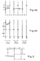
- Fig. 4 illustrates diagrammatically a film composed of alternate layers of two different materials, for example two types of PDA, which have different values of electron affinity A, differing by AA. Different PDA's of different side groups, have energy gaps differing by up to 0.25 eV and corresponding differences occur also in A. Thus AA can be as large as 10 times the thermal energy K B T (at room temperature). The jump times denoted in Figs. 4a and 4b are then
- alternating layers bits can be written into the device with the high field applied, stored for a time up to ⁇ 12 (s) with the field small or zero, and read out of the device with the high field re-applied.
- This alternating layer device is more complicated than the original device because the applied field now has to be controlled, i.e. it must be turned on and off in synchronism with the bits entering and leaving, but the information holding time is longer.
- the bits can be written and read at the same time of the multilayer using EAD, since the bits will move in opposite directions under the influence of the two fields.
- the last bit in will be the first bit out. If reading and writing are to be done at separate times, using the long hold time of the alternating layer device, it is possible to abandon EAD and use CD instead.
- the hold time can be increased by lowering the temperature and so lengthening T , 2 (s) until it equals T" .
- T 140K
- the hold time would be 2.17 hours. Further lowering of the temperature leaves the hold time unaffected.
- the first is the hold time before diffusion destroys the bit pattern when the field is on and the bits are being written in or read out.
- This time sets the maximum write-read time; i.e. it sets the maximum byte length as limited by diffusion.
- the second hold time is the time the bit pattern is retained statically in small or zero field before diffusion destroys the bit pattern.
- These hold times may be referred to respectively as the dynamic hold time and the static hold time.
- the dynamic hold time can be lengthened by using the previously described technique of storing one bit in M layers of which one has high A and (M-1) have low A. This exponentially lengthens ⁇ 11 which is the upper limit to the static hold time which can be reached on lowering the temperature.
- the electrodes both apply the electric field across the device and also supply the transit electrons from the D layer and collect the transit electrons at the F layer.
- They can be metals or doped semiconductors. They can be substrates onto which LB layers are deposited; or they can be evaporated or sputtered onto such LB layers. For semiconductor electrodes with photon energies below the semiconductor band-gap the electrode is transparent; otherwise the electrode is semitransparent (and opaque if thick).
- the layer D forming the electron photo-injector can be a metal, in which case D is also the electrode.
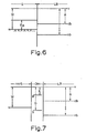
- the metal electrode is denoted M and the LB layer as LB.
- v is the reference energy of an unbound electron at rest
- cb is the conduction band edge of the material of the LB layer (e.g. PDA) at an energy A below V
- vb is the valence band edge of PDA or an energy I below V
- w is the Fermi level of the metal at an energy W below v.
- the available range of W is large so w D can virtually be chosen at will.
- Suitable metals for use as metal electrodes on PDA crystals include Ag, Al, Au, Cd, Cu, Ga, Hg, In, Mg, Pb, Zn, Sn.
- Alternatively D can be a p-type semiconductor, in which case it is also the electrode.
- Suitable semiconductors include Ge, Si, GaAs, GaSb, InP, InAs, InSb, HgTe.
- D is a dye molecule DM, shown in Fig. 7.
- the dye is a strong absorber of photons of energy (G-E), creating an exciton at energy level e.
- the exciton can auto-ionise to create an electron at level cb and a hole at level w if (G-E)>W-A.
- the net result of the photon absorption is electron injection.
- the auto-ionisation will only be efficient if DM is a mono- layer. LB monolayers of dye molecules can be produced, as is mentioned below in reference to the layer F.
- Fig. 7 Another possibility is for D to be a dye molecule DM, shown in Fig. 7.
- the dye is a strong absorber of photons of energy (G-E), creating an exciton at energy level e.
- the exciton can auto-ionise to create an electron at level cb and a hole at level w if (G-E)>W-A.
- w is the Fermi level of a metal or the valence band edge of a semiconductor, depending on whether the electrode is a metal M or a semiconductor S
- g is the electronic ground slate of the dye DM at energy G below V
- e is the first singlet excition state of the dye at energy E below v
- the other symbols have the same meaning as in Figs. 5 and 6.
- the electron arrival detector F can be a p-type semiconductor as shown in Fig. 8.
- the electron arriving at this electrode can enter the conduction band of the semiconductor provided W-E G >A.
- the electron is then a minority carrier in the p-type semiconductor and can recombine rapidly by emission of a photo of energy EG.
- the conditions for such recombination are identical to those required in a semiconductor laser or light-emitting diode, and thus well established.
- F is then analogous to an LED with the n-type electron injector replaced by the PDA multilayer. It is necessary that W ⁇ I so that dark injection of holes does not occur.
- F can be a dye molecule.
- Fig. 9 shows creation of the exciton by tunnelling of the arriving electron to the electrode. This process requires W-A>(G-E), and that F be a monolayer for efficiency. The subsequent rapid dye fluorescence is the signature of the electron arrival:
- the symbols in Fig. 9 have the same meaning as in Fig. 7.
- Fig. 10 shows a further scheme not relying on such a tunnelling process in a monolayer, and which would work with thicker dye layers.
- the symbols have the same meaning as in Fig. 9.
- the process involves the following steps:
- Step 1 occurs spontaneously in the dark and creates positively charged dye molecules. In other than a monolayer of dye and the positive charge will migrate in the applied field to the dye molecules adjacent to the PDA.
- the arriving electron which is highly mobile along the PDA chain, can then hunt in the plane of the film and find the positively charged dye molecule.
- Step 2 the electron enters the dye and forms the exciton.
- Step 3 is the rapid dye fluorescence. Migration of this exciton can be prevented by the methods described above.
- Fluorescing dyes in the required range have been studied at length for their use in dye lasers.
- Dyes can be put in layers by evaporation. If a dye of suitable values of E and G is incorporated in a molecule from which LB layers can be formed, then the dye can be put as mono- or multilayer at the D or F side of the PDA multilayer.
- LB layers can be formed from lightly substituted anthracene derivatives with aliphatic side chains, for example a derivative where the side chain has four CH2 units (known as C4) and a derivative where it has six CH2 units (known as C6). Attention is directed in this connection to the Journal Phys. Technol. Vol. 12, 1981 pp 69 to 87.
- LB films can be formed of derivatives of perylene to obtain perylene fluorescence in the same way.
- the layers of the memory as being of PDA.
- other materials which form LB films can be used instead.
- these are large conjugated organic molecules, because in such molecules the value of I-A is small and there is therefore less chance of impurity and defect trapping of the electrons destroying the spatial coherence of the memory.
- the molecules C4 and C6 mentioned above might be used for the memory, as might a derivative of perylene.
- suitable materials include compounds of the formula where m and n are integers.
- Film-forming compounds of this general formula are known where the values of (m,n) are (12,8), (10,8) (14,8), (16,2) or (16,0).
- a plurality of independent information holding devices can be created in unit area of a film. Three ways in which this can be done are:
Landscapes
- Physics & Mathematics (AREA)
- Spectroscopy & Molecular Physics (AREA)
- General Physics & Mathematics (AREA)
- Semiconductor Memories (AREA)
- Optical Recording Or Reproduction (AREA)
- Bipolar Transistors (AREA)
- Light Receiving Elements (AREA)
Claims (17)
Applications Claiming Priority (2)
| Application Number | Priority Date | Filing Date | Title |
|---|---|---|---|
| GB8130024 | 1981-10-05 | ||
| GB8130024 | 1981-10-05 |
Publications (2)
| Publication Number | Publication Date |
|---|---|
| EP0077135A1 EP0077135A1 (fr) | 1983-04-20 |
| EP0077135B1 true EP0077135B1 (fr) | 1986-05-07 |
Family
ID=10524958
Family Applications (1)
| Application Number | Title | Priority Date | Filing Date |
|---|---|---|---|
| EP82304985A Expired EP0077135B1 (fr) | 1981-10-05 | 1982-09-22 | Dispositif de stockage d'information comportant un film multicouche de Langmuir-Blodgett |
Country Status (5)
| Country | Link |
|---|---|
| US (1) | US4534015A (fr) |
| EP (1) | EP0077135B1 (fr) |
| JP (1) | JPS58141495A (fr) |
| DE (1) | DE3271021D1 (fr) |
| GB (1) | GB2108757A (fr) |
Families Citing this family (16)
| Publication number | Priority date | Publication date | Assignee | Title |
|---|---|---|---|---|
| GB8308309D0 (en) * | 1983-03-25 | 1983-05-05 | Qmc Ind Res | Information holding device |
| GB8409022D0 (en) * | 1984-04-06 | 1984-05-16 | Qmc Ind Res | Information holding device |
| JPH0770690B2 (ja) * | 1986-01-14 | 1995-07-31 | オリンパス光学工業株式会社 | 三次元トンネルメモリ装置 |
| EP0238759B1 (fr) * | 1986-03-25 | 1992-03-11 | Kabushiki Kaisha Toshiba | Procédé pour inscrire de l'information optique |
| EP0268370B1 (fr) * | 1986-10-13 | 1995-06-28 | Canon Kabushiki Kaisha | Commutateur |
| DE3752099T2 (de) * | 1986-12-24 | 1997-11-13 | Canon Kk | Aufzeichnungsgerät und Wiedergabegerät |
| GB8712057D0 (en) * | 1987-05-21 | 1987-06-24 | British Petroleum Co Plc | Optical modulators |
| JP2756254B2 (ja) * | 1988-03-25 | 1998-05-25 | キヤノン株式会社 | 記録装置及び再生装置 |
| US5270965A (en) * | 1988-03-28 | 1993-12-14 | Canon Kabushiki Kaisha | Method of driving device having metal-insulator-metal(mim)structure |
| JP2680849B2 (ja) * | 1988-08-29 | 1997-11-19 | オリンパス光学工業株式会社 | 三次元メモリ素子およびその制御方法 |
| US5033404A (en) * | 1988-10-26 | 1991-07-23 | Nima Technology Ltd. | Barrier mechanism for isolating drive chain from active chamber in Langmuir trough |
| GB8913417D0 (en) * | 1989-06-10 | 1989-08-02 | Emi Plc Thorn | Verification device for a security system |
| EP0411640A3 (en) * | 1989-08-04 | 1992-07-15 | Olympus Optical Co., Ltd. | Three-dimensional integrated memory |
| JP2821194B2 (ja) * | 1989-09-25 | 1998-11-05 | オリンパス光学工業株式会社 | 電荷転送素子とその駆動方法 |
| US5246740A (en) * | 1990-01-12 | 1993-09-21 | Matsushita Electric Industrial Co., Ltd. | Process for preparing a lamination of organic monomolecular films, and a chemical adsorbent used for the process |
| US5539100A (en) * | 1993-07-01 | 1996-07-23 | The United States Of America As Represented By The United States Department Of Energy | Organic solid state switches incorporating porphyrin compounds and method for producing organic solid state optical switches |
Family Cites Families (3)
| Publication number | Priority date | Publication date | Assignee | Title |
|---|---|---|---|---|
| US2833936A (en) * | 1956-01-04 | 1958-05-06 | Ibm | Electrooptical shift register system |
| NL7309000A (fr) * | 1973-06-28 | 1974-12-31 | ||
| US4431263A (en) * | 1979-06-25 | 1984-02-14 | University Patents, Inc. | Novel nonlinear optical materials and processes employing diacetylenes |
-
1982
- 1982-09-20 US US06/420,000 patent/US4534015A/en not_active Expired - Fee Related
- 1982-09-22 EP EP82304985A patent/EP0077135B1/fr not_active Expired
- 1982-09-22 DE DE8282304985T patent/DE3271021D1/de not_active Expired
- 1982-09-22 GB GB08227014A patent/GB2108757A/en not_active Withdrawn
- 1982-10-05 JP JP57174076A patent/JPS58141495A/ja active Pending
Also Published As
| Publication number | Publication date |
|---|---|
| JPS58141495A (ja) | 1983-08-22 |
| EP0077135A1 (fr) | 1983-04-20 |
| DE3271021D1 (en) | 1986-06-12 |
| US4534015A (en) | 1985-08-06 |
| GB2108757A (en) | 1983-05-18 |
Similar Documents
| Publication | Publication Date | Title |
|---|---|---|
| EP0077135B1 (fr) | Dispositif de stockage d'information comportant un film multicouche de Langmuir-Blodgett | |
| US4627029A (en) | Information holding device | |
| Ball et al. | Science at the atomic scale. | |
| Weibel et al. | Functional molecules in electronic circuits | |
| Bässler | Injection, transport and recombination of charge carriers in organic light‐emitting diodes | |
| US5136212A (en) | Electron emitting device, electron generator employing said electron emitting device, and method for driving said generator | |
| US4819210A (en) | Optical information writing method | |
| Gesquiere et al. | F− V/SMS: A New Technique for Studying the Structure and Dynamics of Single Molecules and Nanoparticles | |
| JP3303470B2 (ja) | 蛍光方法、蛍光装置、表示装置、スイッチング装置、蛍光記録方法、蛍光記録媒体、蛍光記録読み出し方法、蛍光記録読み出し装置及び蛍光記録消去方法 | |
| JPH0693258A (ja) | 有機薄膜素子 | |
| Yamaguchi et al. | Transport properties of photoexcited carriers in a fibonacci superlattice | |
| JPH05129645A (ja) | 光・電子デバイスを有する装置 | |
| Kranzelbinder et al. | Picosecond spectroscopy and hyperlinear photoluminescence in poly (para-phenylene)-type ladder polymers | |
| Tkachenko et al. | Photoelectric signals of chlorophyll a Langmuir-Blodgett films | |
| Bondar et al. | Arrays of size-dispersed ZnSe quantum dots as artificial antennas: Role of quasi-coherent regime and in-gap states of excitons for enhanced light harvesting and energy transfer | |
| Neubauer et al. | Local cathode luminescence resonant peak in hybrid organic nanocrystal systems | |
| Nagamura et al. | Transient photocurrents in monolayer assemblies containing amphipathic porphyrin upon excitation with a dye laser | |
| Moses | Charge quantum yield and transient transport properties of anthracene and amorphous selenium | |
| Lin et al. | Electronic process in organic solids | |
| US7196364B2 (en) | Molecular device, molecule array, rectifier device, rectifying method, sensor device, switching device, circuit device, logical circuit device, operational device and information processing device | |
| Uddin et al. | CdSe/ZnS Quantum dot size dependent carrier relaxation in hybrid organic/inorganic system | |
| Schroeder | Characterization of organic and inorganic optoelectronic semiconductor devices using advanced spectroscopic methods | |
| Greenham | Electrical properties of semiconductor nanocrystals | |
| Ebler et al. | Electrical detection of excitonic states by time-resolved conductance measurements | |
| Querner et al. | Fluorescence dynamics of semiconductor nanorod clusters studied by correlated atomic force, transmission electron, and fluorescence microscopy |
Legal Events
| Date | Code | Title | Description |
|---|---|---|---|
| PUAI | Public reference made under article 153(3) epc to a published international application that has entered the european phase |
Free format text: ORIGINAL CODE: 0009012 |
|
| AK | Designated contracting states |
Designated state(s): CH DE FR GB LI NL |
|
| 17P | Request for examination filed |
Effective date: 19830609 |
|
| GRAA | (expected) grant |
Free format text: ORIGINAL CODE: 0009210 |
|
| AK | Designated contracting states |
Kind code of ref document: B1 Designated state(s): CH DE FR GB LI NL |
|
| PG25 | Lapsed in a contracting state [announced via postgrant information from national office to epo] |
Ref country code: NL Effective date: 19860507 Ref country code: LI Effective date: 19860507 Ref country code: FR Free format text: THE PATENT HAS BEEN ANNULLED BY A DECISION OF A NATIONAL AUTHORITY Effective date: 19860507 Ref country code: CH Effective date: 19860507 |
|
| REF | Corresponds to: |
Ref document number: 3271021 Country of ref document: DE Date of ref document: 19860612 |
|
| REG | Reference to a national code |
Ref country code: CH Ref legal event code: PL |
|
| EN | Fr: translation not filed | ||
| NLV1 | Nl: lapsed or annulled due to failure to fulfill the requirements of art. 29p and 29m of the patents act | ||
| PLBE | No opposition filed within time limit |
Free format text: ORIGINAL CODE: 0009261 |
|
| STAA | Information on the status of an ep patent application or granted ep patent |
Free format text: STATUS: NO OPPOSITION FILED WITHIN TIME LIMIT |
|
| 26N | No opposition filed | ||
| PG25 | Lapsed in a contracting state [announced via postgrant information from national office to epo] |
Ref country code: DE Effective date: 19870602 |
|
| GBPC | Gb: european patent ceased through non-payment of renewal fee | ||
| PG25 | Lapsed in a contracting state [announced via postgrant information from national office to epo] |
Ref country code: GB Effective date: 19881121 |