EP0077862B1 - Procédé de caractérisation du comportement en fiabilité de dispositifs semi-conducteurs bipolaires - Google Patents
Procédé de caractérisation du comportement en fiabilité de dispositifs semi-conducteurs bipolaires Download PDFInfo
- Publication number
- EP0077862B1 EP0077862B1 EP81430036A EP81430036A EP0077862B1 EP 0077862 B1 EP0077862 B1 EP 0077862B1 EP 81430036 A EP81430036 A EP 81430036A EP 81430036 A EP81430036 A EP 81430036A EP 0077862 B1 EP0077862 B1 EP 0077862B1
- Authority
- EP
- European Patent Office
- Prior art keywords
- time
- eff
- determining
- manufacturing line
- reliability
- Prior art date
- Legal status (The legal status is an assumption and is not a legal conclusion. Google has not performed a legal analysis and makes no representation as to the accuracy of the status listed.)
- Expired
Links
Images

Classifications
-
- G—PHYSICS
- G01—MEASURING; TESTING
- G01R—MEASURING ELECTRIC VARIABLES; MEASURING MAGNETIC VARIABLES
- G01R31/00—Arrangements for testing electric properties; Arrangements for locating electric faults; Arrangements for electrical testing characterised by what is being tested not provided for elsewhere
- G01R31/28—Testing of electronic circuits, e.g. by signal tracer
- G01R31/2851—Testing of integrated circuits [IC]
- G01R31/2855—Environmental, reliability or burn-in testing
- G01R31/2856—Internal circuit aspects, e.g. built-in test features; Test chips; Measuring material aspects, e.g. electro migration [EM]
- G01R31/2858—Measuring of material aspects, e.g. electro-migration [EM], hot carrier injection
-
- G—PHYSICS
- G01—MEASURING; TESTING
- G01R—MEASURING ELECTRIC VARIABLES; MEASURING MAGNETIC VARIABLES
- G01R31/00—Arrangements for testing electric properties; Arrangements for locating electric faults; Arrangements for electrical testing characterised by what is being tested not provided for elsewhere
- G01R31/26—Testing of individual semiconductor devices
- G01R31/2607—Circuits therefor
- G01R31/2608—Circuits therefor for testing bipolar transistors
-
- G—PHYSICS
- G01—MEASURING; TESTING
- G01R—MEASURING ELECTRIC VARIABLES; MEASURING MAGNETIC VARIABLES
- G01R31/00—Arrangements for testing electric properties; Arrangements for locating electric faults; Arrangements for electrical testing characterised by what is being tested not provided for elsewhere
- G01R31/26—Testing of individual semiconductor devices
- G01R31/2642—Testing semiconductor operation lifetime or reliability, e.g. by accelerated life tests
-
- H—ELECTRICITY
- H10—SEMICONDUCTOR DEVICES; ELECTRIC SOLID-STATE DEVICES NOT OTHERWISE PROVIDED FOR
- H10W—GENERIC PACKAGES, INTERCONNECTIONS, CONNECTORS OR OTHER CONSTRUCTIONAL DETAILS OF DEVICES COVERED BY CLASS H10
- H10W10/00—Isolation regions in semiconductor bodies between components of integrated devices
- H10W10/01—Manufacture or treatment
- H10W10/031—Manufacture or treatment of isolation regions comprising PN junctions
-
- H—ELECTRICITY
- H10—SEMICONDUCTOR DEVICES; ELECTRIC SOLID-STATE DEVICES NOT OTHERWISE PROVIDED FOR
- H10W—GENERIC PACKAGES, INTERCONNECTIONS, CONNECTORS OR OTHER CONSTRUCTIONAL DETAILS OF DEVICES COVERED BY CLASS H10
- H10W10/00—Isolation regions in semiconductor bodies between components of integrated devices
- H10W10/30—Isolation regions comprising PN junctions
Definitions
- the present invention relates to the field of semiconductor integrated circuits and more particularly to a method for characterizing the reliability behavior of bipolar semiconductor devices, manufactured on a given line and using a given technology, according to the first Part of claim 1.
- other, potential faults which can only be detected later after a certain operating time For example, the well known phenomenon of electromigration of aluminum grains in aluminum conductors, which causes, by the accumulation of these grains, the bursting of the covering silica layer.
- the problem of electromigration has received an elegant solution with the use of an aluminum-copper metallurgy, we can in particular refer to the document US ⁇ A ⁇ 3,725,309 (IBM). Defects of the latter type are called reliability and they are often catastrophic because they require intervention in machines installed in customers with all the disadvantages that this entails.
- the aim of reliability studies is therefore to accelerate the ripening of these potential defects which deteriorate over time, and to highlight them before the marketing of microchips.
- the microchips produced during manufacture are fixed to ceramic substrates to constitute electronic modules.
- These modules are in turn mounted on cards which include other auxiliary circuits and provide the measurement functions for a certain number of parameters.
- the cards are placed "under constraints", that is to say that they are introduced into an oven while voltages are applied to them, which can be the different nominal operating voltages of said modules (this is the process known as "burn in”).
- the temperature of the oven and the duration of the operation depend on the nature of the chips. Baking times of the order of 1000 hours (three weeks) are completely normal.
- the failure time T time to fail
- the failure time T is defined as the time taken for a failure to occur. happen. If for example after 500 hours of steaming, we have 50% of the modules that are faulty, we will say that the T 50 is 500 hours.
- the semiconductor industry therefore needs a method for characterizing the reliability of bipolar devices which preferably is carried out at the chip level and no longer at the module level, and which avoids having to resort to the step steaming (which involves the generation of special cards and extremely long lead times).
- the present invention as characterized in claim 1 proposes to solve this problem, by experimentally establishing a correlation between certain so-called predominant parameters among the electrical parameters characterizing the charges in the oxide, grouped in a reliability function R, and the reliability results provided in the form of a failure time, for example the T 50 .
- This experimental study having shown that these instability phenomena come essentially from two, among the numerous physical and electrical parameters, which characterize the passivation oxide, namely the number of charges in the oxide and the density of interface states.
- test structure and this is one of the advantages of the invention, is constituted simply, from a parasitic PNP transistor, as it was mentioned above, and which has been used as an FET transistor, the isolation region, acting as source, the base region, drain and the base contact, acting as door electrode (it is connected to the drain).
- the method of the present invention which provides direct and rapid determination of the failure time (for example the T 5o ), by simple electrical measurements, firstly comprises preliminary steps for calibrating the production line in question. These steps consist in: developing on said production line, bipolar semiconductor devices comprising at least one FET type test structure; selecting a plurality of these devices; the calculation for each of the devices 'selected from the test structure, a reliability function R equal to the product N SS .
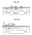
- FIG. 1A there is shown a conventional NPN bipolar transistor comprising emitter, base and collector regions, sub-collector and collector crossing regions, formed in a box isolated from the epitaxial layer by isolation regions.
- the reliability fault results from a leakage current which is established in the parasitic transistor, between the two P-type regions.
- this leakage current had due to instabilities in the charge of the passivation oxide.
- An FET transistor is therefore used, the source region of which is constituted by the upper isolation region and the drain by the base region of the NPN transistor; the surface of the epitaxial layer located between these regions forms the channel region.
- the FET transistor shown in FIG. 1B constitutes the test structure. The only constraint is that the threshold voltage V T of the FET must be less than the breakdown voltage of the junction, to make the measurements possible.
- the leakage current which appears between the two regions P seems to result from the presence of charges induced on the surface of the silicon. That is to say, it can be created by mobile charges in the oxide or by injection of carriers from silicon. A negative charge is however necessary at the Si-Si0 2 interface to create a conductive path in the silicon.
- Such a condition can occur when there are negative mobile ions in the oxide which can drift towards the interface during baking; stationary negative ions, neutralized by positive mobile ions, which can drift from the interface leaving a negative charge in place, injecting electrons from silicon to the oxide and trapping the electrons in the oxide.
- the leakage current did not depend on the physical parameters of the oxide (density, quality, etc.) but on certain electrical parameters N eff (charge density in the oxide), N ss (density d 'interface states) and, N D (concentration of the epitaxial layer), hereinafter called preponderant parameters which alone characterized both the electronic current which occurs during steaming (composed of the diffusion current, the recombination current at the interface, the electron emission current from silicon to the oxide created by electronic emission and by tunnel effect) and the trapping of electrons in the oxide (depending on the number of traps, etc.).
- the V r of the test FET transistor shown in FIG. 1B is measured and it is biased at a slightly lower voltage (for example two volts).
- the equations which describe the behavior of the FET, in weak inversion are known in the literature, one can in particular refer to the article: "Inadequacy of the Classical Theory of the MOS Transistor Under Weak Inversion" by RJ Van Overstraeten et al., IEEE Trans. On Electron Devices, Vol. ED20, December 1973.
- the FET is polarized so that it is in strong inversion, and therefore in saturation.
- the equations that govern the FET under these conditions can be found in the following reference: NATO: “Advanced Study Institute for IC Design” July 19-29, 1977 FM Klaasen-Review of Physical Models for MOS Transistor. Published by the clergy University of Louvain.
- the threshold voltage V T in saturation V TS is provided by the relation: expression in which V S is the potential of the source region, ⁇ F the Fermi potential at equilibrium, ⁇ ms the metal-silicon output work, Q ox the equivalent charge of the oxide and k a known coefficient such that : where ⁇ si is the permittivity of silicon.
- N eff is a function of E ox (through C ox ) and of N D (through k), so we can write:
- N D is a parameter of the process and that it is in principle known from the specification. This measurement is only for a more precise determination.
- the problem is to determine E ox .
- ⁇ ox is the permittivity of the oxide
- ⁇ P the mobility of the holes
- W and L represent respectively the width and the length of the FET device (see Figure 1B).
- the quantities W and L are determined from an optical measurement, and I is determined by calculation.
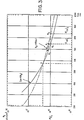
- Figure 3 shows in a real particular case, the shape of these curves, the intersection of curves H and 1 provides the solutions E ox and N D (in the case shown in Figure 3, we find E ox ⁇ 570 nm and N D ⁇ 2,210 16 atoms / cm 3. The values found for E ox and N D are reported in equation (8), hence the determination of N eff , and in equation (4) for the determination of N SS .
- FIG. 4 The block diagram of the calculation of the preponderant parameters of the reliability function R, that is to say N eff , N o and N ss is shown in FIG. 4.
- the presence of block 21 means that all the starting data which results direct measurements, both electrical (V TS1 , V TS2 . V S1 , V S2 , ⁇ , s ...) and optical (W, L) are developed to constitute the working database.
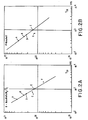
- the standard product corresponded practically to batch C of FIG. 2A whereas the product after annealing in hydrogen is reference in F on this same figure, and has a T 50 of 2000 hours. This improvement was therefore detected immediately, the calculation of the reliability function being carried out quickly using the calculation technique described below (part III and FIG. 4). This variant in the annealing step could be implemented immediately on the production line.
Landscapes
- Engineering & Computer Science (AREA)
- Physics & Mathematics (AREA)
- General Physics & Mathematics (AREA)
- Microelectronics & Electronic Packaging (AREA)
- Environmental & Geological Engineering (AREA)
- Computer Hardware Design (AREA)
- General Engineering & Computer Science (AREA)
- Testing Or Measuring Of Semiconductors Or The Like (AREA)
- Testing Of Individual Semiconductor Devices (AREA)
- Bipolar Transistors (AREA)
Priority Applications (4)
| Application Number | Priority Date | Filing Date | Title |
|---|---|---|---|
| EP81430036A EP0077862B1 (fr) | 1981-10-28 | 1981-10-28 | Procédé de caractérisation du comportement en fiabilité de dispositifs semi-conducteurs bipolaires |
| DE8181430036T DE3173901D1 (en) | 1981-10-28 | 1981-10-28 | Process for characterising the reliability behaviour of bipolar semiconductor devices |
| JP57135806A JPS5879732A (ja) | 1981-10-28 | 1982-08-05 | バイポ−ラ半導体装置の診断方法 |
| US06/435,139 US4520448A (en) | 1981-10-28 | 1982-10-18 | Method of characterizing reliability in bipolar semiconductor devices |
Applications Claiming Priority (1)
| Application Number | Priority Date | Filing Date | Title |
|---|---|---|---|
| EP81430036A EP0077862B1 (fr) | 1981-10-28 | 1981-10-28 | Procédé de caractérisation du comportement en fiabilité de dispositifs semi-conducteurs bipolaires |
Publications (2)
| Publication Number | Publication Date |
|---|---|
| EP0077862A1 EP0077862A1 (fr) | 1983-05-04 |
| EP0077862B1 true EP0077862B1 (fr) | 1986-02-26 |
Family
ID=8188600
Family Applications (1)
| Application Number | Title | Priority Date | Filing Date |
|---|---|---|---|
| EP81430036A Expired EP0077862B1 (fr) | 1981-10-28 | 1981-10-28 | Procédé de caractérisation du comportement en fiabilité de dispositifs semi-conducteurs bipolaires |
Country Status (4)
| Country | Link |
|---|---|
| US (1) | US4520448A (ja) |
| EP (1) | EP0077862B1 (ja) |
| JP (1) | JPS5879732A (ja) |
| DE (1) | DE3173901D1 (ja) |
Families Citing this family (26)
| Publication number | Priority date | Publication date | Assignee | Title |
|---|---|---|---|---|
| IT1215273B (it) * | 1985-05-09 | 1990-01-31 | Ates Componenti Elettron | Procedimento e dispositivo per identificare transistori parassiti in una struttura integrata. |
| US4860080A (en) * | 1987-03-31 | 1989-08-22 | General Electric Company | Isolation for transistor devices having a pilot structure |
| US5646540A (en) * | 1989-04-19 | 1997-07-08 | Interuniversitair Micro-Elektronic Centrum Vzw | Apparatus and method for measuring electromagnetic ageing parameter of a circuit element and predicting its values |
| US5262672A (en) * | 1989-08-09 | 1993-11-16 | National Semiconductor Corporation | Apparatus for improvement of interconnection capacitance |
| US5107320A (en) * | 1989-08-09 | 1992-04-21 | National Semiconductor Corporation | Method and apparatus for improvement of interconnection capacitance |
| US5410490A (en) * | 1991-09-03 | 1995-04-25 | Hewlett-Packard Company | Electromigration verification method and apparatus |
| US5519336A (en) * | 1992-03-03 | 1996-05-21 | Honeywell Inc. | Method for electrically characterizing the insulator in SOI devices |
| US5325054A (en) * | 1992-07-07 | 1994-06-28 | Texas Instruments Incorporated | Method and system for screening reliability of semiconductor circuits |
| US5394101A (en) * | 1993-01-15 | 1995-02-28 | National Semiconductor Corporation | Method for detecting mobile ions in a semiconductor device |
| US5600578A (en) * | 1993-08-02 | 1997-02-04 | Advanced Micro Devices, Inc. | Test method for predicting hot-carrier induced leakage over time in short-channel IGFETs and products designed in accordance with test results |
| US5598102A (en) * | 1993-08-19 | 1997-01-28 | Texas Instruments Incorporated | Method for detecting defects in semiconductor insulators |
| JPH07130817A (ja) * | 1993-10-30 | 1995-05-19 | Sony Corp | 金属配線の信頼性評価方法及び金属配線の信頼性評価装置 |
| US5486772A (en) * | 1994-06-30 | 1996-01-23 | Siliconix Incorporation | Reliability test method for semiconductor trench devices |
| US5485097A (en) * | 1994-08-08 | 1996-01-16 | Advanced Micro Devices, Inc. | Method of electrically measuring a thin oxide thickness by tunnel voltage |
| JP3206374B2 (ja) * | 1995-06-19 | 2001-09-10 | 松下電器産業株式会社 | 回路機能ブロックの信頼性試験方法 |
| DE19610065A1 (de) * | 1996-03-14 | 1997-09-18 | Siemens Ag | Verfahren zur Abschätzung der Lebensdauer eines Leistungshalbleiter-Bauelements |
| WO1998045719A1 (en) | 1997-04-04 | 1998-10-15 | University Of Florida | Method for testing and diagnosing mos transistors |
| US5986281A (en) * | 1997-10-23 | 1999-11-16 | Lucent Technologies, Inc. | Circuit and method for predicting failure rates in a semiconductor device |
| US6425111B1 (en) * | 1999-12-30 | 2002-07-23 | The Board Of Trustees Of The Leland Stanford Junior University | Saturation region transistor modeling for geometric programming |
| CN100375257C (zh) * | 2003-05-23 | 2008-03-12 | 上海宏力半导体制造有限公司 | 用以厘清漏电流发生原因的半导体测试结构 |
| JP4675043B2 (ja) * | 2003-12-26 | 2011-04-20 | 株式会社豊田中央研究所 | バイポーラトランジスタ、バイポーラトランジスタの特性変動モデル式特定方法、及びバイポーラトランジスタの良否判定方法 |
| US7298159B1 (en) * | 2005-07-07 | 2007-11-20 | National Semiconductor Corporation | Method of measuring the leakage current of a deep trench isolation structure |
| US8935143B2 (en) | 2010-12-15 | 2015-01-13 | IP Cube Partners Co., Ltd. | Semiconductor sensor reliability |
| US8680523B2 (en) | 2010-12-16 | 2014-03-25 | IP Cube Partners (ICP) Co., Ltd. | Sensor for semiconductor degradation monitoring and modeling |
| RU2694169C1 (ru) * | 2018-12-21 | 2019-07-09 | Федеральное государственное бюджетное образовательное учреждение высшего образования "Национальный исследовательский Мордовский государственный университет им. Н.П. Огарёва" | Способ определения предельной величины блокирующего напряжения силовых транзисторов |
| US11754625B2 (en) * | 2020-01-30 | 2023-09-12 | Kla Corporation | System and method for identifying latent reliability defects in semiconductor devices |
Family Cites Families (7)
| Publication number | Priority date | Publication date | Assignee | Title |
|---|---|---|---|---|
| US3335340A (en) * | 1964-02-24 | 1967-08-08 | Ibm | Combined transistor and testing structures and fabrication thereof |
| US3889188A (en) * | 1973-07-30 | 1975-06-10 | Ibm | Time zero determination of FET reliability |
| US3939381A (en) * | 1974-03-22 | 1976-02-17 | Mcm Industries, Inc. | Universal burn-in fixture |
| GB1559583A (en) * | 1975-07-18 | 1980-01-23 | Tokyo Shibaura Electric Co | Complementary mosfet device and method of manufacturing the same |
| US4180439A (en) * | 1976-03-15 | 1979-12-25 | International Business Machines Corporation | Anodic etching method for the detection of electrically active defects in silicon |
| US4144493A (en) * | 1976-06-30 | 1979-03-13 | International Business Machines Corporation | Integrated circuit test structure |
| US4281449A (en) * | 1979-12-21 | 1981-08-04 | Harris Corporation | Method for qualifying biased burn-in integrated circuits on a wafer level |
-
1981
- 1981-10-28 EP EP81430036A patent/EP0077862B1/fr not_active Expired
- 1981-10-28 DE DE8181430036T patent/DE3173901D1/de not_active Expired
-
1982
- 1982-08-05 JP JP57135806A patent/JPS5879732A/ja active Granted
- 1982-10-18 US US06/435,139 patent/US4520448A/en not_active Expired - Fee Related
Also Published As
| Publication number | Publication date |
|---|---|
| JPS5879732A (ja) | 1983-05-13 |
| US4520448A (en) | 1985-05-28 |
| JPS632141B2 (ja) | 1988-01-18 |
| EP0077862A1 (fr) | 1983-05-04 |
| DE3173901D1 (en) | 1986-04-03 |
Similar Documents
| Publication | Publication Date | Title |
|---|---|---|
| EP0077862B1 (fr) | Procédé de caractérisation du comportement en fiabilité de dispositifs semi-conducteurs bipolaires | |
| FR2593640A1 (fr) | Dispositif semi-conducteur monolithique integre comportant des transistors a jonction bipolaire, des transistors cmos et dmos, des diodes a faible fuite et procede pour sa fabrication | |
| US9627502B2 (en) | Circuit arrangement and method of forming a circuit arrangement | |
| CN101926005B (zh) | 用于消除多晶硅/金属板电容器中的工艺相关缺陷的结构及方法 | |
| KR20090074206A (ko) | 반도체 웨이퍼의 평가방법 | |
| EP0797252B1 (fr) | Substrat de type silicium sur isolant pour la fabrication de transistors et procédé de préparation d'un tel substrat | |
| JP5751531B2 (ja) | 半導体基板の評価方法、評価用半導体基板、半導体装置 | |
| JP5434491B2 (ja) | 半導体基板の評価方法及び半導体デバイスの製造方法 | |
| JP5967019B2 (ja) | 半導体ウェーハの評価方法 | |
| US5841294A (en) | Method for measuring leakage current in junction region of semiconductor device | |
| EP3772093A1 (fr) | Procédé de fabrication comprenant une définition d'une longueur effective de canal de transistors mosfet | |
| US7335518B2 (en) | Method for manufacturing semiconductor device | |
| FR3136109A1 (fr) | Dispositif semiconducteur du type silicium sur isolant et procédé de fabrication correspondant | |
| Jerome et al. | The effect of trench processing conditions on complementary bipolar analog devices with SOI/Trench isolation | |
| FR3066025A1 (fr) | Procede de caracterisation electrique de transistor mos sur soi | |
| US7351595B2 (en) | Method for manufacturing semiconductor device | |
| JP3163756B2 (ja) | 半導体装置および半導体装置の製造方法 | |
| US20060267118A1 (en) | Semiconductor device and method of manufacturing the same | |
| JPH10509276A (ja) | Cmos集積回路用のエピタキシャル半導体ウエーハ | |
| US7043328B2 (en) | Method for manufacturing semiconductor device utilizing monitor wafers | |
| FR3057104A1 (fr) | Transistors a effet de champ de type fdsoi | |
| JP3303833B2 (ja) | 半導体装置及びその製造方法 | |
| FR2667726A1 (fr) | Dispositif a semi-conducteur ayant une couche d'arret de canal dopee double et procede de fabrication. | |
| JP2005150208A (ja) | Soiウェーハの評価方法 | |
| CN119069348A (zh) | 绝缘栅双极晶体管的制造方法 |
Legal Events
| Date | Code | Title | Description |
|---|---|---|---|
| PUAI | Public reference made under article 153(3) epc to a published international application that has entered the european phase |
Free format text: ORIGINAL CODE: 0009012 |
|
| 17P | Request for examination filed |
Effective date: 19811125 |
|
| AK | Designated contracting states |
Designated state(s): DE FR GB |
|
| GRAA | (expected) grant |
Free format text: ORIGINAL CODE: 0009210 |
|
| AK | Designated contracting states |
Designated state(s): DE FR GB |
|
| REF | Corresponds to: |
Ref document number: 3173901 Country of ref document: DE Date of ref document: 19860403 |
|
| PLBE | No opposition filed within time limit |
Free format text: ORIGINAL CODE: 0009261 |
|
| STAA | Information on the status of an ep patent application or granted ep patent |
Free format text: STATUS: NO OPPOSITION FILED WITHIN TIME LIMIT |
|
| 26N | No opposition filed | ||
| PGFP | Annual fee paid to national office [announced via postgrant information from national office to epo] |
Ref country code: DE Payment date: 19911102 Year of fee payment: 11 |
|
| PGFP | Annual fee paid to national office [announced via postgrant information from national office to epo] |
Ref country code: FR Payment date: 19920928 Year of fee payment: 12 |
|
| PG25 | Lapsed in a contracting state [announced via postgrant information from national office to epo] |
Ref country code: DE Effective date: 19930701 |
|
| PGFP | Annual fee paid to national office [announced via postgrant information from national office to epo] |
Ref country code: GB Payment date: 19930922 Year of fee payment: 13 |
|
| PG25 | Lapsed in a contracting state [announced via postgrant information from national office to epo] |
Ref country code: FR Effective date: 19940630 |
|
| REG | Reference to a national code |
Ref country code: FR Ref legal event code: ST |
|
| PG25 | Lapsed in a contracting state [announced via postgrant information from national office to epo] |
Ref country code: GB Effective date: 19941028 |
|
| GBPC | Gb: european patent ceased through non-payment of renewal fee |
Effective date: 19941028 |