EP0079209B1 - Verfahren zum Antreiben eines thermischen Kopfes - Google Patents
Verfahren zum Antreiben eines thermischen Kopfes Download PDFInfo
- Publication number
- EP0079209B1 EP0079209B1 EP82305888A EP82305888A EP0079209B1 EP 0079209 B1 EP0079209 B1 EP 0079209B1 EP 82305888 A EP82305888 A EP 82305888A EP 82305888 A EP82305888 A EP 82305888A EP 0079209 B1 EP0079209 B1 EP 0079209B1
- Authority
- EP
- European Patent Office
- Prior art keywords
- shift register
- picture data
- data
- serial
- inputted
- Prior art date
- Legal status (The legal status is an assumption and is not a legal conclusion. Google has not performed a legal analysis and makes no representation as to the accuracy of the status listed.)
- Expired
Links
Images

Classifications
-
- H—ELECTRICITY
- H04—ELECTRIC COMMUNICATION TECHNIQUE
- H04N—PICTORIAL COMMUNICATION, e.g. TELEVISION
- H04N1/00—Scanning, transmission or reproduction of documents or the like, e.g. facsimile transmission; Details thereof
- H04N1/04—Scanning arrangements, i.e. arrangements for the displacement of active reading or reproducing elements relative to the original or reproducing medium, or vice versa
- H04N1/19—Scanning arrangements, i.e. arrangements for the displacement of active reading or reproducing elements relative to the original or reproducing medium, or vice versa using multi-element arrays
- H04N1/191—Scanning arrangements, i.e. arrangements for the displacement of active reading or reproducing elements relative to the original or reproducing medium, or vice versa using multi-element arrays the array comprising a one-dimensional [1D] array
- H04N1/192—Simultaneously or substantially simultaneously scanning picture elements on one main scanning line
- H04N1/193—Simultaneously or substantially simultaneously scanning picture elements on one main scanning line using electrically scanned linear arrays, e.g. linear CCD arrays
- H04N1/1931—Simultaneously or substantially simultaneously scanning picture elements on one main scanning line using electrically scanned linear arrays, e.g. linear CCD arrays with scanning elements electrically interconnected in groups
-
- H—ELECTRICITY
- H03—ELECTRONIC CIRCUITRY
- H03M—CODING; DECODING; CODE CONVERSION IN GENERAL
- H03M9/00—Parallel/series conversion or vice versa
Definitions
- the present invention relates to a method of, and an apparatus for, driving a thermal head used for thermal recording.
- a thermal head is selectively driven to cause a portion of a sheet of thermosensitive paper placed in contact with the thermal head to generate color to record information thereon.
- a number of heating elements are aligned in the thermal head. It is not efficient to separately drive these heating elements at different times in view of recording speed requirements. Accordingly, in ordinary recording apparatus, a plurality of heating elements are simultaneously driven. To this end in such an apparatus, serial picture data is inputted to a shift register and then converted therein into parallel picture data is response to which the heating elements are driven. In the case where the heating elements are grouped and to be driven group after group a number times per one line in such an apparatus, however it is necessary to replace old picture data set in the shift register by new data a corresponding number times for one line.
- a counter has been provided in the conventional apparatus to count every time pieces of picture data corresponding to the number of the heating elements to be driven simultaneously have been inputted to the shift register and produce a signal indicating the completion of setting of data.
- the transfer of the picture data to the shift register is stopped and then restarted after the driving of the concerned heating elements has been attained.
- the replacement of picture data in the shift register has been achieved in this manner.
- FR-A-2 461 413 there is shown an apparatus for driving an electric styli printing head which uses a counter to count picture elements as they are input to a shift register.
- US-A-3 946 379 describes a serial-to-parallel converter circuit for devices such as computers which handle digital information as groups of bits, called characters or bytes. Such a group of bits commonly comprises a start bit, a set of data bits, and one or more stop bits.
- serial data is converted to parallel data in a shift register.
- the circuit detects the presence of a start bit on an input line and this serially clocks data into the shift register.
- clocking the serial data into the shift register is terminated and a strobe signal is produced to indicate the availability of a complete character in the shift register for parallel shifting out.
- this document does not show how to eliminate a counter converting serial picture data in a thermal recording apparatus. Such serial data is not divided into groups each of which commences with a start bit.
- An object of the present invention is to provide, in order to eliminate the above-mentioned drawback, a method of, and an apparatus for, driving a thermal head in which it is not necessary to provide any counter for counting the picture data inputted to a shift register even in the case where all the heating elements are grouped into plural blocks and driven block after block.
- a method of driving a thermal head in which serial picture data to be recorded on one line is inputted to a shift register which produces parallel picture data corresponding to said input serial picture data to drive heating elements of the thermal head by said parallel picture data characterized in that said method comprises the steps of inputting serial picture data into a plurality of one line buffer memories, transferring serial picture data from said buffer memories to said shift register, gating the data flow from said buffer memories into said shift register so that, when serial picture data is inputted into said shift register from one of said buffer memories, new serial picture data is inputted into another one of said buffer memories, applying a data reset signal to said shift register to clear the contents thereof following the driving of the thermal head and before inputting new serial picture data, adding a distinguishing data element in front of said serial picture data as it is transferred from a buffer memory to said shift register, said data distinguishing element being derived from said data reset signal, determining a time frame which follows the time when a predetermined amount of picture data to be simultaneously recorded has been inputted
- an apparatus for driving a thermal head having heating elements comprising a shift register which receives serial picture data to be recorded on one line and produces parallel picture data corresponding to said serial picture data to drive said heating elements
- said apparatus further comprises a plurality of one line buffer memories for receiving said serial picture data, gating means for transferring serial picture data from said buffer memories to said shift register so that, when serial picture data is inputted into said shift register from one of said buffer memories, new serial picture data is inputted into another one of said buffer memories, means for applying a data reset signal to said shift register to clear the contents thereof following the driving of the thermal head and before inputting new serial picture, means for adding a distinguishing data element derived from said data reset signal in front of said serial picture data as it is transferred from a buffer memory to said shift register, means for determining a time frame when a predetermined amount of picture data to be simultaneously recorded has been inputted to said shift register by detecting the presence of said distinguishing data element at an output terminal of said shift register, means for
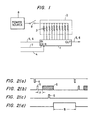
- a shift register 1 is connected to a plurality of heating elements 3 of a thermal head 2 which are to be simultaneously driven.
- a data reset signal 4 is applied to a reset terminal R of the shift register 1 in a timing relationship shown in Fig. 2(a) in advance to the transfer of picture data.
- the shift register 1 is reset in response to the data reset signal 4.
- a dummy bit 5 and picture data 6 are successively supplied in this order to a data input terminal IN of the shift register 1 (Fig. 2(b)), in accordance with a clock signal 7 supplied to a clock input terminal CK of the shift register 1.
- the dummy bit 5 and the picture data 6 are shifted in the shift register 1 in response to the clock signal 7 until the dummy bit 5 is outputted from a data output terminal OUT (Fig. 2(c)).
- the recording apparatus stops the input of the picture data 6 at this time and connects the heater elements 3 to a power source 8 through a switch 9 so that the thermal head 2 is driven for a predetermined period B (Fig. 2(d)). Thereafter, the contents of the shift register 1 are cleared by the data reset signal 4, so that the same operation discussed above may be repeated to achieve thermosensitive recording on the recording paper.
- Fig. 3 shows a recording apparatus comprising a thermal head 11 for attaining recording by recording twice, one portion after another on every line.
- the thermal head 11 is provided with two blocks of heater elements, and a shift register driver integrated circuit 13.
- the respective blocks of heater elements 12, and 12 z are aligned at an interval of 8 dots/mm along a distance of 216 mm.
- the shift register driver 13 is an integrated circuit constituted by a shift register having a bit capacity of 864 bits and a switching circuit for driving the heater elements 12, and 12 2 .
- Such IC's are well known in this technology.
- the recording apparatus comprises two one-line buffers 14, and 14 2 that are arranged such that when picture data 17 for a certain line is being inputted into one of the one-line buffers, picture data 18 for one previous line comes out of the other one-line buffer, by the actuation of the change-over switches 15 and 16 provided at the input side of each of the one-line buffers 14, and 14 2 and at the output side of the same, respectively.
- a sequencer 21 receives a phase signal 19 generated for every line in synchronism with the change-over of the change-over switches 15 and 16 and produces a data reset signal 22 after the lapse of a predetermined time from the reception of the phase signal 19.
- the data reset signal 22 is supplied to a reset terminal R of the shift register driver IC 13 to clear picture data which has been used for the previous recording.
- the data reset signal 22 is also applied to a first delay circuit 24 through an inverter 23 and delayed by 0.5 ps therein to be formed into a dummy bit 25.
- the dummy bit 25 is supplied not only to a second delay circuit 26 but to a data input terminal IN of the shift register driver IC 13 through an OR circuit 27.
- the second delay circuit 26 delays the dummy bit 25 by a slight time to form a dummy bit input clock signal 28.
- the dummy bit input clock signal 28 is applied not only to the sequencer 21 but also to a clock input terminal CK of the shift register driver IC 13.
- the dummy bit 25 is inputted to the shift register driver IC 13.
- the sequencer 21 detects this timing by the dummy bit input clock signal 28 to produce 1 MHz clock signal 31 for actuating the shift register driver IC 13 to start the data shifting sequence.
- the clock signal 31 is also applied to the first and second one-line buffers 14, and 14 2 .
- the first one-line buffer 14 When in a status where the change-over switch 16 is selecting the first one-line buffer 14, as shown in Fig. 2, the first one-line buffer 14, outputs the picture data 18.
- the picture data 18 is applied to the data input terminal IN of the shift register driver IC 13 through the OR circuit 27, and inputted to and shifted in the shift register driver IC 13 in synchronism with the clock signal 31 applied to the clock input terminal CK through the OR circuit 29.
- the sequencer 21 stops the sending-out of the clock signal 31 after the lapse of 4 ps from the time when the dummy bit 25 has been outputted from the shift register driver IC 13.
- the transfer of the picture data 18 from the first one-line buffer 14 1 is stopped and the shifting of data in the shift register driver IC 13 is also stopped.
- 864 bits of picture data have been inputted to the shift register driver IC 13.
- a power source 32 is connected to the 864 number of heating elements 12 1 through one of the contacts of a switch 33 which is now actuated as shown in Fig. 3, the heating elements 12 1 are selected allowed to pass a current to generate heat, so that the thermosensitive recording is attained on one-half of one line.
- the sequencer 21 produces a data reset signal at a predetermined time to clear the data in the shift register driver IC 13.
- picture data for the remainder half of the one line is inputted into the shift register driver IC 13.
- the switch 33 is actuated at this time, to close the other contact to connect the power source 32 to the heater elements 12 2 , thereby accomplishing the thermosensitive recording on the remainder half of the one line.
- thermosensitive recording on one line Upon the completion of thermosensitive recording on one line, the change-over switches 15 and 16 are actuated to output from the second one-line buffer 14 2 a picture data. A phase signal 19 is supplied to the sequencer 21 so that the series of operations as mentioned above are restarted.
- the picture data inputted into a shift register is controlled without using a counter, there are advantages that the components or parts constituting the apparatus may be reduced in number and the apparatus may be accordingly improved by its reliability.
- the present invention is not limited to the method. Further, although a shift register driver IC is used in the embodiment, it is possible to replace the shift register driver IC by a shift register and a driver circuit which are separately provided as individual devices.
Landscapes
- Engineering & Computer Science (AREA)
- Theoretical Computer Science (AREA)
- Multimedia (AREA)
- Signal Processing (AREA)
- Electronic Switches (AREA)
- Facsimile Heads (AREA)
Claims (5)
Applications Claiming Priority (2)
| Application Number | Priority Date | Filing Date | Title |
|---|---|---|---|
| JP56177132A JPS5881183A (ja) | 1981-11-06 | 1981-11-06 | サ−マルヘツド駆動方法 |
| JP177132/81 | 1981-11-06 |
Publications (3)
| Publication Number | Publication Date |
|---|---|
| EP0079209A2 EP0079209A2 (de) | 1983-05-18 |
| EP0079209A3 EP0079209A3 (en) | 1984-08-29 |
| EP0079209B1 true EP0079209B1 (de) | 1986-08-27 |
Family
ID=16025731
Family Applications (1)
| Application Number | Title | Priority Date | Filing Date |
|---|---|---|---|
| EP82305888A Expired EP0079209B1 (de) | 1981-11-06 | 1982-11-05 | Verfahren zum Antreiben eines thermischen Kopfes |
Country Status (4)
| Country | Link |
|---|---|
| US (1) | US4477820A (de) |
| EP (1) | EP0079209B1 (de) |
| JP (1) | JPS5881183A (de) |
| DE (1) | DE3272931D1 (de) |
Families Citing this family (5)
| Publication number | Priority date | Publication date | Assignee | Title |
|---|---|---|---|---|
| JPH0377473A (ja) * | 1989-08-21 | 1991-04-03 | Ricoh Co Ltd | 画像情報記憶装置 |
| US5315320A (en) * | 1990-09-29 | 1994-05-24 | Kyocera Corporation | Mirror image printing printhead |
| US5805195A (en) * | 1996-03-26 | 1998-09-08 | Oyo Instruments, Inc. | Diode-less thermal print head and method of controlling same |
| JP4688281B2 (ja) * | 2000-12-01 | 2011-05-25 | 富士通コンポーネント株式会社 | サーマルヘッド |
| JP4873905B2 (ja) * | 2005-09-01 | 2012-02-08 | 富士通コンポーネント株式会社 | サーマルヘッド駆動方法及びサーマルヘッド駆動回路 |
Family Cites Families (6)
| Publication number | Priority date | Publication date | Assignee | Title |
|---|---|---|---|---|
| US3946379A (en) * | 1974-05-31 | 1976-03-23 | Rca Corporation | Serial to parallel converter for data transmission |
| US4141018A (en) * | 1976-11-08 | 1979-02-20 | Tokyo Shibaura Electric Co., Ltd. | Thermal recording head and drive circuit |
| CA1089921A (en) * | 1977-10-24 | 1980-11-18 | Steven Kos | Printer with moving printing head |
| US4284953A (en) * | 1977-12-23 | 1981-08-18 | Motorola, Inc. | Character framing circuit |
| FR2461413A1 (fr) * | 1979-07-13 | 1981-01-30 | Cit Alcatel | Circuit de commande de stylets d'une barrette d'impression d'image |
| JPS56109068A (en) * | 1980-02-04 | 1981-08-29 | Nippon Telegr & Teleph Corp <Ntt> | Recorder for multitone |
-
1981
- 1981-11-06 JP JP56177132A patent/JPS5881183A/ja active Pending
-
1982
- 1982-11-05 EP EP82305888A patent/EP0079209B1/de not_active Expired
- 1982-11-05 DE DE8282305888T patent/DE3272931D1/de not_active Expired
- 1982-11-08 US US06/440,061 patent/US4477820A/en not_active Expired - Lifetime
Also Published As
| Publication number | Publication date |
|---|---|
| EP0079209A2 (de) | 1983-05-18 |
| DE3272931D1 (en) | 1986-10-02 |
| EP0079209A3 (en) | 1984-08-29 |
| US4477820A (en) | 1984-10-16 |
| JPS5881183A (ja) | 1983-05-16 |
Similar Documents
| Publication | Publication Date | Title |
|---|---|---|
| US3984844A (en) | Thermal recording apparatus | |
| EP0068702B1 (de) | Thermischer Drucker | |
| US2932688A (en) | Electrical storage of intelligence | |
| US5646672A (en) | Thermal head apparatus | |
| EP0295953B1 (de) | Druckverfahren für thermische Drucker | |
| EP0061314B1 (de) | Wärmeempfindliches Aufzeichnungsgerät | |
| EP0079209B1 (de) | Verfahren zum Antreiben eines thermischen Kopfes | |
| EP0113250B1 (de) | Thermodruckkopf | |
| US4415904A (en) | Thermal head driving method | |
| US4224641A (en) | Abnormality indication system of facsimile apparatus | |
| EP0016457B1 (de) | Apparat zum Aufzeichnen der auf einer Kathodenstrahlröhre angezeigten Daten | |
| US4510506A (en) | Recording apparatus | |
| CA2034964C (en) | Printer | |
| JPS61230466A (ja) | ライン型サ−マルヘツド駆動方法 | |
| EP0378201B1 (de) | Drucker | |
| JPS58161465A (ja) | 記録制御方式 | |
| SU1319042A1 (ru) | Устройство дл управлени и обмена данными | |
| JPS6322763Y2 (de) | ||
| JP2858442B2 (ja) | 記録ヘッド駆動装置 | |
| JPH0379371A (ja) | 印字制御回路 | |
| JPH0434864B2 (de) | ||
| JPH07304201A (ja) | プリントヘッド駆動ic | |
| JPS6313390B2 (de) | ||
| JPH01249365A (ja) | 感熱記録制御方式 | |
| KR20060010426A (ko) | 열전사헤드의 구동방법 및 장치 |
Legal Events
| Date | Code | Title | Description |
|---|---|---|---|
| PUAI | Public reference made under article 153(3) epc to a published international application that has entered the european phase |
Free format text: ORIGINAL CODE: 0009012 |
|
| AK | Designated contracting states |
Designated state(s): DE FR GB |
|
| PUAL | Search report despatched |
Free format text: ORIGINAL CODE: 0009013 |
|
| AK | Designated contracting states |
Designated state(s): DE FR GB |
|
| 17P | Request for examination filed |
Effective date: 19840711 |
|
| GRAA | (expected) grant |
Free format text: ORIGINAL CODE: 0009210 |
|
| AK | Designated contracting states |
Kind code of ref document: B1 Designated state(s): DE FR GB |
|
| ET | Fr: translation filed | ||
| REF | Corresponds to: |
Ref document number: 3272931 Country of ref document: DE Date of ref document: 19861002 |
|
| PLBE | No opposition filed within time limit |
Free format text: ORIGINAL CODE: 0009261 |
|
| STAA | Information on the status of an ep patent application or granted ep patent |
Free format text: STATUS: NO OPPOSITION FILED WITHIN TIME LIMIT |
|
| 26N | No opposition filed | ||
| PGFP | Annual fee paid to national office [announced via postgrant information from national office to epo] |
Ref country code: GB Payment date: 19961028 Year of fee payment: 15 |
|
| PGFP | Annual fee paid to national office [announced via postgrant information from national office to epo] |
Ref country code: DE Payment date: 19961108 Year of fee payment: 15 |
|
| PGFP | Annual fee paid to national office [announced via postgrant information from national office to epo] |
Ref country code: FR Payment date: 19961111 Year of fee payment: 15 |
|
| PG25 | Lapsed in a contracting state [announced via postgrant information from national office to epo] |
Ref country code: GB Free format text: LAPSE BECAUSE OF NON-PAYMENT OF DUE FEES Effective date: 19971105 |
|
| PG25 | Lapsed in a contracting state [announced via postgrant information from national office to epo] |
Ref country code: FR Free format text: THE PATENT HAS BEEN ANNULLED BY A DECISION OF A NATIONAL AUTHORITY Effective date: 19971130 |
|
| GBPC | Gb: european patent ceased through non-payment of renewal fee |
Effective date: 19971105 |
|
| PG25 | Lapsed in a contracting state [announced via postgrant information from national office to epo] |
Ref country code: DE Free format text: LAPSE BECAUSE OF NON-PAYMENT OF DUE FEES Effective date: 19980801 |
|
| REG | Reference to a national code |
Ref country code: FR Ref legal event code: ST |