EP0080058B1 - Structure intermédiaire utilisée dans la fabrication de dispositifs semi-conducteurs, procédé pour la fabrication de transistors à effet de champ et transistors - Google Patents
Structure intermédiaire utilisée dans la fabrication de dispositifs semi-conducteurs, procédé pour la fabrication de transistors à effet de champ et transistors Download PDFInfo
- Publication number
- EP0080058B1 EP0080058B1 EP82109508A EP82109508A EP0080058B1 EP 0080058 B1 EP0080058 B1 EP 0080058B1 EP 82109508 A EP82109508 A EP 82109508A EP 82109508 A EP82109508 A EP 82109508A EP 0080058 B1 EP0080058 B1 EP 0080058B1
- Authority
- EP
- European Patent Office
- Prior art keywords
- layer
- central
- forming
- layers
- central layer
- Prior art date
- Legal status (The legal status is an assumption and is not a legal conclusion. Google has not performed a legal analysis and makes no representation as to the accuracy of the status listed.)
- Expired
Links
Images








Classifications
-
- H—ELECTRICITY
- H10—SEMICONDUCTOR DEVICES; ELECTRIC SOLID-STATE DEVICES NOT OTHERWISE PROVIDED FOR
- H10D—INORGANIC ELECTRIC SEMICONDUCTOR DEVICES
- H10D30/00—Field-effect transistors [FET]
- H10D30/01—Manufacture or treatment
- H10D30/061—Manufacture or treatment of FETs having Schottky gates
-
- H—ELECTRICITY
- H10—SEMICONDUCTOR DEVICES; ELECTRIC SOLID-STATE DEVICES NOT OTHERWISE PROVIDED FOR
- H10D—INORGANIC ELECTRIC SEMICONDUCTOR DEVICES
- H10D30/00—Field-effect transistors [FET]
- H10D30/80—FETs having rectifying junction gate electrodes
- H10D30/87—FETs having Schottky gate electrodes, e.g. metal-semiconductor FETs [MESFET]
- H10D30/871—Vertical FETs having Schottky gate electrodes
-
- H—ELECTRICITY
- H10—SEMICONDUCTOR DEVICES; ELECTRIC SOLID-STATE DEVICES NOT OTHERWISE PROVIDED FOR
- H10D—INORGANIC ELECTRIC SEMICONDUCTOR DEVICES
- H10D62/00—Semiconductor bodies, or regions thereof, of devices having potential barriers
- H10D62/10—Shapes, relative sizes or dispositions of the regions of the semiconductor bodies; Shapes of the semiconductor bodies
- H10D62/17—Semiconductor regions connected to electrodes not carrying current to be rectified, amplified or switched, e.g. channel regions
- H10D62/213—Channel regions of field-effect devices
- H10D62/221—Channel regions of field-effect devices of FETs
-
- H—ELECTRICITY
- H10—SEMICONDUCTOR DEVICES; ELECTRIC SOLID-STATE DEVICES NOT OTHERWISE PROVIDED FOR
- H10D—INORGANIC ELECTRIC SEMICONDUCTOR DEVICES
- H10D62/00—Semiconductor bodies, or regions thereof, of devices having potential barriers
- H10D62/80—Semiconductor bodies, or regions thereof, of devices having potential barriers characterised by the materials
- H10D62/82—Heterojunctions
-
- H—ELECTRICITY
- H10—SEMICONDUCTOR DEVICES; ELECTRIC SOLID-STATE DEVICES NOT OTHERWISE PROVIDED FOR
- H10D—INORGANIC ELECTRIC SEMICONDUCTOR DEVICES
- H10D62/00—Semiconductor bodies, or regions thereof, of devices having potential barriers
- H10D62/80—Semiconductor bodies, or regions thereof, of devices having potential barriers characterised by the materials
- H10D62/82—Heterojunctions
- H10D62/824—Heterojunctions comprising only Group III-V materials heterojunctions, e.g. GaN/AlGaN heterojunctions
-
- H—ELECTRICITY
- H10—SEMICONDUCTOR DEVICES; ELECTRIC SOLID-STATE DEVICES NOT OTHERWISE PROVIDED FOR
- H10P—GENERIC PROCESSES OR APPARATUS FOR THE MANUFACTURE OR TREATMENT OF DEVICES COVERED BY CLASS H10
- H10P50/00—Etching of wafers, substrates or parts of devices
- H10P50/60—Wet etching
- H10P50/61—Electrolytic etching
- H10P50/617—Electrolytic etching of Group III-V materials
Definitions
- the invention relates to a field effect transistor and a method of making a field effect transistor.
- the invention seeks to enable the production of transistors and other semiconductor devices having extremely small dimensions.
- a field effect transistor having a vertical structure and comprising a central channel region forming a heterojunction with each of a pair of outer regions which serve as the source and the drain, and a gate electrode functionally associated with the channel region, the channel region being in the form of a web connecting the pair of outer regions and of a material which has an electron energy work function substantially equal to that of the material of at least one of the outer regions, and having a thickness of the order of magnitude of the transport length of a charge carrier in the semiconductor material which it is composed of.
- a method of making a field effect transistor in a portion of a monocrystalline semiconductor body having a first outer layer, a central layer and a second outer layer each of said first and second outer layers being of semiconductor material different from the semiconductor material of the central layer and forming a heterojunction with the central layer, the thickness of said central layer being of the order of magnitude of the transport length of a charge carrier in the semiconductor material of that layer, and at least two adjacent layers of the body having substantially equal electron energy work functions; the method comprising removing areas of the second outer and central layers on each side of said portion, removing an area of the second outer layer at one end of said portion, etching the central layer of said portion to form a web connecting the first and second outer layers of said portion, forming insulation on the exposed surfaces of the first and second outer layers, forming a Schottky barrier electrode on the web and providing electrical contacts to the first and second outer layers of said portion.
- One of the most critical dimensions in semiconductors is the carrier transport length of the region of the device which charge carriers, either majority or minority, must traverse between junctions.
- Many of the limitations on device fabrication are related to deleterious effects on this dimension caused by processing step degradation, heat, or impurity location imprecision.
- an intermediate structure consists of a monocrystalline semiconductor member 1 having at least three layers 2, 3 and 4.
- the outer layers 2 and 4 are of a semiconductor material different from that of the central layer 3 and make respective semiconductor carrier responsive heterojunctions 5 and 6 with the central layer 3.
- the layer 3 thickness between the junctions 5 and 6 is the carrier transport dimension in the final semiconductor device.
- FIG. 2 there is shown the result of a processing operation wherein through the upper surface an opening 8 is made that exposes both the layer 2 and the layer 3 and permits a device to be fabricated in an elongate portion 9 having a precise carrier transport dimension already established by the thickness of layer 3 and external contacting capability established by layers 2 and 4 and the exposed portion of layer 3.
- This intermediate structure permits a number of processing advantages. It permits low temperature fabrication, photoetch thinning, selective oxidation and selective plating.
- One particular device advantage is the ability to minimize work function differences between regions of a field effect transistor device.
- a field effect transistor (FET) structure can be provided wherein multiple semiconductor materials having carefully selected work functions operate to prevent boundary limitations between regions of the device such that limits are avoided on how short the field effect channel can be.
- a structure is provided wherein the work function is the same in all the regions of the device. This permits the energy band edges to change abruptly in going from one region to another and permits the electron concentration profile to also change abruptly. The result of this is that allowance does not have to be made for the boundary carrier condition from one device to the other and the dimensions can be held to much tighter tolerances. This is of importance in the integrated circuit technology wherein the difference between one-half micron gate width in a device and one micron gate width may make the difference between 64,000 and 128,000 devices per one square one-eighth inch (3.2 mm).
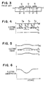
- a conventional field effect transistor is shown wherein a source region 10 is adjacent to a channel region 11 which in turn is adjacent to a drain region 12, the source and drain regions being labelled n + indicative of higher conductivity and the lower conductivity channel region being labelled n, as is conventional in the art.
- the regions are made in a substrate and have ohmic contacts 13, 14 and 15, respectively, to the source, channel and drain.
- Figs. 4, 5 and 6 are electron energy and concentration diagrams taken along the line A-A' of Fig. 3 with the assumptions that the sections of the device are separated in Fig. 3 and the electron affinity X having subscripts 10, 11 and 12 is the same for all three regions whereas the work function labelled ⁇ with subscripts 10, 11 and 12 for the regions may differ since it goes from the vacuum level to the Fermi level.
- FIG. 3 A prior art type structure as illustrated in Fig. 3 would have constraints on the dimensions of the channel relaxed with the work function matching technique as set forth in Figs. 7 through 10.
- a source region 16 a channel region 17 and a drain region 18 in standard field effect transistor relationships wherein the regions 16, 17 and 18 correspond respectively to layers 2, 3 and 4 of Fig. 1.
- the device is a heterojunction device in which at least two of the regions are of different semiconductor materials.
- region 16, region 17 and region 18 are of different semiconductor materials, chosen such that the work function of all three are the same.
- the structure of Fig. 7 also shows the channel region 17 as having gate electrodes 19 and 20, respectively, on each side which can be used to reduce either channel resistance or device area or both compared with the conventional device of Fig. 3.
- Fig. 7 The structure of Fig. 7 is made up of different semiconductor materials so chosen that the electron work function as shown in Fig. 8 in each of the regions isequal as set forth in Equation 1, the components of which are obtained from Equations 2, 3 and 4.
- an electron energy diagram is provided for the structure of Fig. 7 wherein the subscripts 16, 17 and 18 are employed.
- the energy diagram is taken along the line B-B' of Fig. 7 with the assumption that the sections of the device are separated.
- the materials of the various regions are chosen so that the work functions ⁇ 16 , ( ⁇ 17 and ⁇ 18 are equal whereas the electron affinities may differ.
- the effect of this on the structure may be seen in connection with Fig. 9 wherein the electron energy is shown, assuming the sections of the device are now adjacent to each other.
- the energy band diagram permits the band edges to change abruptly in going from one region to another and some of the physical dimension of the central channel region does not have to be allowed for the variation in band energy.
- the electron concentration changes abruptly in going from one region to another so that the electron concentration in the channel region is not influenced by the regions adjacent to it and this may be compared with Fig. 6 wherein the electron concentration is significantly influenced by the regions adjacent to it.
- This process employs as a starting substrate a member as shown in Fig. 1 having at least two types of layers in a three-layer structure, the central layer of which has the transport dimension established by the positioning of the heterojunction between layers.
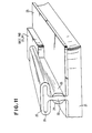
- a source region 21 of a vertical field effect type transistor corresponds to the lowermost region 2 of the three-layered substrate 1 of Fig. 1.
- the channel region 22 is a thin vertical web fabricated from the central layer 3 of Fig. 1 on which gate metal regions 23 and 24 have been deposited.
- An insulating oxide 25 is provided over region 21.
- the drain region 26 is the layer 4 of the starting structure 1 of Fig. 1.
- An insulating oxide 27 is provided over the drain region 26. Source and drain ohmic contacts (not shown) are made to the source 21 and drain 26 regions.
- the thickness of the web of the gate region 22 is achieved using a self-limiting technique such as that described in published European Patent application EP 37876 A2.
- a self-limiting technique such as that described in published European Patent application EP 37876 A2.
- an electrochemical etching operation using photogenerated carriers is employed to establish the desired dimension and the process self-limits at the appropriate size.
- the oxides 25 and 27 are grown using an anodic oxidation technique since the regions 21 and 26 are conductive.
- Fig. 12 an intermediate process step is illustrated wherein the starting structure of Fig. 1 is provided having three epitaxial layers 2, 3 and 4, respectively, on a handling facilitating substrate 28 which is semi-insulating.
- the uppermost layer 4 is made of a material with a wider bandgap than the bandgap of the central layer 3.
- the materials for the three layers 2, 3 and 4 are chosen so as to minimize any built-in potential and to optimize the crystal lattice match between the adjacent layers.
- Each layer 2, and 4 may be doped uniformly so long as the effect on work function between regions is recognized.
- Fig. 1 is formed by epitaxial growth, standard impurity inclusion during the growth stages is provided.
- layers 2 and 4 may be heavily doped n', for example, to provide low resistivity source 21 and drain 26 regions and for the vertical web channel structure 22 an n doping concentration will be maintained in the layer 3. This will impart the desirable current-voltage circuit characteristics to the gate junctions to the channel region 22 which are Schottky barrier junctions between the metal members 23 and 24 and the channel web 22.
- the thickness of the layer 3 has been chosen to provide the desired carrier transport dimension for the type of device being built. In the device of Fig. 11 the thickness of the layer 3 will give the desired field effect device channel length.
- the thickness of the layers 2 and 4 are chosen in order to optimize the stress relief produced by any crystalline lattice spacing mismatch at the n' n heterojunctions and to minimize electrical resistance.
- Layer 4 may be 0.2 micrometers thick, layer 3 may be 0.2 micrometers thick and layer 2 may be 1.5 micrometers thick.
- a resist mask has been formed on the upper surface 29 and openings 30 and 31 have been etched through both layers 4 and 3 on each side of a region that is to be the channel 22.
- the mask patterns should be so designed that after the etching, the layer 4 will be still electrically continuous to the edge of the semiconductor member, or electrically continuous through some path where more complex structures are being manufactured, so that an applied electrical bias may be used during the later etching process when the specific thickness of the channel region 22 in the layer 3 is defined, during the anodic oxidation when layers 27 and 25 are grown, or during the electroplating operation when the gate metal layer 23 and 24 is applied.
- each of the layers 2, 3 and 4 is composed of a different material so that one can be etached independently of the other. This facilitates and provides self-alignment of an underlying edge to the one above and it also prevents accidental etching of underlying areas through defects in a mask.
- FIG. 12 The view through the openings 30 and 31 in Fig. 12 illustrates both the cross-sectional and the top down view of the structure as illustrated in Fig. 11 after completion of the processing to this point.
- FIG. 13 another intermediate process condition is illustrated to facilitate explanation of processing of dimensions of and contacts to the central layer.
- An area 32 is opened through layer 4 such as by etching through a mask on surface 29 with an etch that attacks the material of layer 4 thereby exposing a portion of layer 3 joining openings 30 and 31 of Fig. 12.
- Proton bombardment, ion implantation or further etch thinning may be employed in the area of layer 3 in opening 32 immediately adjacent one end of the channel wherein gate contacts are to be placed. This is done to make the exposed portion of layer 4 in opening 32 semi-insulating prior to deposit of metal thereon.
- the structure in the condition of Fig. 13 is next placed in an electrolytic bath, not shown, while under the influence of a voltage bias between the etch bath and the layer 3 in the presence of illumination by light 33 focused on the area to produce the channel thickness 22 of Fig. 11.
- the light 33 is of a proper wavelength to penetrate the layer 4 and be absorbed in the layer 3.
- the absorbed light produces in layer 3 photogenerated carriers that provide free minority carriers to support an electrolytic etching current.
- the etching operation will proceed to the dotted lines 34 and will self-stop when the layer 3 is etched thin enough so that it is completely depleted of carriers.
- the target value of thickness 22 is achieved without the aid of a bias.
- a voltage bias between the etch bath and the layer 3 may be applied in order to select the precise thickness and therefore the FET device electrical threshold voltage.
- metal is then plated on all the exposed unoxidized regions of layer 3 so as to provide a gate contact path through the area of opening 32 of Fig. 13 and the gate Schottky barrier diode connections 23 and 24 on each side of the channel 22 in Fig. 11.
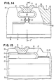
- FIG. 14 there is provided a front view of the structure of Fig. 11 in Fig. 14 and a side view along line C-C' as Fig. 15.
- the two views show the features of the structure of Fig. 11 to illustrate device isolation and some structural aspects.
- the devices may be isolated, by providing non-conducting regions to separate them.
- the isolation is shown as insulation 34 made by etching through all layers to the substrate 28 and then providing insulation such as oxide through the techniques of evaporation, sputtering or spin-on. Alternative techniques, such as proton bombardment or ion implantation, may be used for isolation.
- Metal contacts 35 are provided for circuit purposes by means of contact hole etch and interconnection metallization steps standard in the art. The length, width and thickness of the channel are shown for ease of perception.
- Table 1 a listing of the materials with the essential physical properties and chemical responsiveness to provide two separate structures.
- FIGs. 16A and 16B an illustration is provided of a plurality of the devices of Figs. 11,14 and 15 assembled in a standard circuit known in the art as a "NOR" gate together with the masks for production.
- the circuit diagram of one NOR gate is shown in Fig. 16A.
- the circuit has a separate device for each of three inputs and a load device.
- the current through the load device is delivered to the outputs and the output potential will be high if none of the inputs are supplied with a high potential otherwise the load device current is not available to the output and the output potential will be low.
- the load device in the circuit of Fig. 16A is a depletion mode field effect transistor whereas the input transistors are enhancement mode field effect transistors.
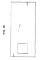
- Fig. 16B there are superimposed six masks that together are used to produce a semiconductor structure of the circuit of Fig. 16A. Each mask is shown individually in Figs. 17 to 21.
- circuit of Fig. 16A employs as an output transistor a depletion mode device, this type of circuit accommodation is accomplished by interchanging the layer of the starting structure to be used for the source and drain.
Landscapes
- Junction Field-Effect Transistors (AREA)
- Bipolar Transistors (AREA)
Claims (11)
Applications Claiming Priority (2)
| Application Number | Priority Date | Filing Date | Title |
|---|---|---|---|
| US324240 | 1981-11-23 | ||
| US06/324,240 US4460910A (en) | 1981-11-23 | 1981-11-23 | Heterojunction semiconductor |
Publications (3)
| Publication Number | Publication Date |
|---|---|
| EP0080058A2 EP0080058A2 (fr) | 1983-06-01 |
| EP0080058A3 EP0080058A3 (en) | 1984-12-27 |
| EP0080058B1 true EP0080058B1 (fr) | 1988-06-01 |
Family
ID=23262711
Family Applications (1)
| Application Number | Title | Priority Date | Filing Date |
|---|---|---|---|
| EP82109508A Expired EP0080058B1 (fr) | 1981-11-23 | 1982-10-14 | Structure intermédiaire utilisée dans la fabrication de dispositifs semi-conducteurs, procédé pour la fabrication de transistors à effet de champ et transistors |
Country Status (4)
| Country | Link |
|---|---|
| US (1) | US4460910A (fr) |
| EP (1) | EP0080058B1 (fr) |
| JP (2) | JPS5892279A (fr) |
| DE (1) | DE3278605D1 (fr) |
Families Citing this family (13)
| Publication number | Priority date | Publication date | Assignee | Title |
|---|---|---|---|---|
| US4550489A (en) * | 1981-11-23 | 1985-11-05 | International Business Machines Corporation | Heterojunction semiconductor |
| FR2520157B1 (fr) * | 1982-01-18 | 1985-09-13 | Labo Electronique Physique | Dispositif semi-conducteur du genre transistor a heterojonction(s) |
| US4551904A (en) * | 1982-02-09 | 1985-11-12 | Trw Inc. | Opposed gate-source transistor |
| FR2548454B1 (fr) * | 1983-07-01 | 1986-12-12 | Labo Electronique Physique | Transistor a effet de champ a grille submicronique presentant une structure verticale |
| GB2162370B (en) * | 1984-07-26 | 1987-10-28 | Japan Res Dev Corp | Static induction transistor and integrated circuit comprising such a transistor |
| JPS6312177A (ja) * | 1986-07-03 | 1988-01-19 | Fujitsu Ltd | 超高周波トランジスタ |
| DE59010851D1 (de) * | 1989-04-27 | 1998-11-12 | Max Planck Gesellschaft | Halbleiterstruktur mit einer 2D-Ladungsträgerschicht und Herstellungsverfahren |
| NL8902292A (nl) * | 1989-09-14 | 1991-04-02 | Philips Nv | Werkwijze voor het vervaardigen van een een mesa bevattende halfgeleiderinrichting. |
| US5385865A (en) * | 1990-04-26 | 1995-01-31 | Max-Planck-Gesellschaft Zur Forderung Der Wissenschaften | Method of generating active semiconductor structures by means of starting structures which have a 2D charge carrier layer parallel to the surface |
| FR2693314B1 (fr) * | 1992-07-02 | 1994-10-07 | Alain Chantre | Transistor JFET vertical à mode de fonctionnement bipolaire optimisé et procédé de fabrication correspondant. |
| US5757038A (en) * | 1995-11-06 | 1998-05-26 | International Business Machines Corporation | Self-aligned dual gate MOSFET with an ultranarrow channel |
| CN1325658C (zh) * | 2001-04-23 | 2007-07-11 | 三星电子株式会社 | 包含mosfet分子检测芯片和采用该芯片的分子检测装置以及使用该装置的分子检测方法 |
| US9287360B1 (en) | 2015-01-07 | 2016-03-15 | International Business Machines Corporation | III-V nanowire FET with compositionally-graded channel and wide-bandgap core |
Family Cites Families (22)
| Publication number | Priority date | Publication date | Assignee | Title |
|---|---|---|---|---|
| US3614549A (en) * | 1968-10-15 | 1971-10-19 | Ibm | A semiconductor recombination radiation device |
| US3982261A (en) * | 1972-09-22 | 1976-09-21 | Varian Associates | Epitaxial indium-gallium-arsenide phosphide layer on lattice-matched indium-phosphide substrate and devices |
| US3833435A (en) * | 1972-09-25 | 1974-09-03 | Bell Telephone Labor Inc | Dielectric optical waveguides and technique for fabricating same |
| US3801391A (en) * | 1972-09-25 | 1974-04-02 | Bell Telephone Labor Inc | Method for selectively etching alxga1-xas multiplier structures |
| US3814993A (en) * | 1972-11-15 | 1974-06-04 | Us Navy | Tuneable infrared photocathode |
| US3958143A (en) * | 1973-01-15 | 1976-05-18 | Varian Associates | Long-wavelength photoemission cathode |
| US4075652A (en) * | 1974-04-17 | 1978-02-21 | Matsushita Electronics Corporation | Junction gate type gaas field-effect transistor and method of forming |
| JPS5168771A (en) * | 1974-12-11 | 1976-06-14 | Matsushita Electric Industrial Co Ltd | Heterokozohandotaino sentakufushokuhoho |
| JPS5828753B2 (ja) * | 1975-08-15 | 1983-06-17 | 株式会社日立製作所 | 縦形電界効果トランジスタの製造方法 |
| JPS5384570A (en) * | 1976-12-29 | 1978-07-26 | Fujitsu Ltd | Field effect semiconductor device and its manufacture |
| US4111725A (en) * | 1977-05-06 | 1978-09-05 | Bell Telephone Laboratories, Incorporated | Selective lift-off technique for fabricating gaas fets |
| US4173763A (en) * | 1977-06-09 | 1979-11-06 | International Business Machines Corporation | Heterojunction tunneling base transistor |
| US4135954A (en) * | 1977-07-12 | 1979-01-23 | International Business Machines Corporation | Method for fabricating self-aligned semiconductor devices utilizing selectively etchable masking layers |
| US4128733A (en) * | 1977-12-27 | 1978-12-05 | Hughes Aircraft Company | Multijunction gallium aluminum arsenide-gallium arsenide-germanium solar cell and process for fabricating same |
| US4364072A (en) * | 1978-03-17 | 1982-12-14 | Zaidan Hojin Handotai Kenkyu Shinkokai | Static induction type semiconductor device with multiple doped layers for potential modification |
| US4198644A (en) * | 1978-06-09 | 1980-04-15 | The United States Of America As Represented By The Secretary Of The Army | Tunnel diode |
| DE2913068A1 (de) * | 1979-04-02 | 1980-10-23 | Max Planck Gesellschaft | Heterostruktur-halbleiterkoerper und verwendung hierfuer |
| US4236166A (en) * | 1979-07-05 | 1980-11-25 | Bell Telephone Laboratories, Incorporated | Vertical field effect transistor |
| US4262296A (en) * | 1979-07-27 | 1981-04-14 | General Electric Company | Vertical field effect transistor with improved gate and channel structure |
| US4226649A (en) * | 1979-09-11 | 1980-10-07 | The United States Of America As Represented By The Secretary Of The Navy | Method for epitaxial growth of GaAs films and devices configuration independent of GaAs substrate utilizing molecular beam epitaxy and substrate removal techniques |
| JPS56124273A (en) * | 1980-03-04 | 1981-09-29 | Semiconductor Res Found | Semiconductor device |
| JPS6048909B2 (ja) * | 1981-05-29 | 1985-10-30 | 富士通株式会社 | 能動的半導体装置及び製造方法 |
-
1981
- 1981-11-23 US US06/324,240 patent/US4460910A/en not_active Expired - Lifetime
-
1982
- 1982-08-20 JP JP57143556A patent/JPS5892279A/ja active Granted
- 1982-10-14 DE DE8282109508T patent/DE3278605D1/de not_active Expired
- 1982-10-14 EP EP82109508A patent/EP0080058B1/fr not_active Expired
-
1987
- 1987-11-20 JP JP62292263A patent/JPS63146472A/ja active Granted
Also Published As
| Publication number | Publication date |
|---|---|
| EP0080058A3 (en) | 1984-12-27 |
| JPS63146472A (ja) | 1988-06-18 |
| DE3278605D1 (en) | 1988-07-07 |
| JPH0126551B2 (fr) | 1989-05-24 |
| US4460910A (en) | 1984-07-17 |
| EP0080058A2 (fr) | 1983-06-01 |
| JPH0355987B2 (fr) | 1991-08-27 |
| JPS5892279A (ja) | 1983-06-01 |
Similar Documents
| Publication | Publication Date | Title |
|---|---|---|
| EP0518683B1 (fr) | Transistor à effet de champ métal-semiconducteur à grande puissance et haute fréquence fabriqué en carbure de silicium | |
| EP0080058B1 (fr) | Structure intermédiaire utilisée dans la fabrication de dispositifs semi-conducteurs, procédé pour la fabrication de transistors à effet de champ et transistors | |
| US4607270A (en) | Schottky barrier diode with guard ring | |
| US4351706A (en) | Electrochemically eroding semiconductor device | |
| JPS62262468A (ja) | 凹入形ゲ−ト半導体デバイスを作製する方法 | |
| JPH0371776B2 (fr) | ||
| US7061067B2 (en) | Schottky barrier diode | |
| US4983536A (en) | Method of fabricating junction field effect transistor | |
| KR890011026A (ko) | 반도체 소자 제조방법 | |
| US4550489A (en) | Heterojunction semiconductor | |
| US5192700A (en) | Method of making field effect transistor | |
| US5126805A (en) | Junction field effect transistor with SiGe contact regions | |
| KR920010671B1 (ko) | 반도체장치 | |
| EP0130774B1 (fr) | Procédé pour la fabrication des transistors bipolaires | |
| GB2103419A (en) | Field effect transistor with metal source | |
| JPS5879773A (ja) | 電界効果トランジスタ | |
| EP0698926B1 (fr) | Thyristor à induction statique normalement non-conducteur | |
| USH291H (en) | Fully ion implanted junction field effect transistor | |
| US5541424A (en) | Permeable base transistor having laminated layers | |
| US5597743A (en) | Method of manufacturing a field effect transistor with improved isolation between electrode | |
| US6902992B2 (en) | Method of fabricating semiconductor device having semiconductor resistance element | |
| KR910006751B1 (ko) | 반도체 집적회로장치 및 그의 제조방법 | |
| GB2151078A (en) | Semiconductor devices | |
| JPS6225456A (ja) | 縦形半導体装置及びその製造方法 | |
| JP3164042B2 (ja) | 半導体装置及びその製造方法 |
Legal Events
| Date | Code | Title | Description |
|---|---|---|---|
| PUAI | Public reference made under article 153(3) epc to a published international application that has entered the european phase |
Free format text: ORIGINAL CODE: 0009012 |
|
| AK | Designated contracting states |
Designated state(s): DE FR GB |
|
| 17P | Request for examination filed |
Effective date: 19830915 |
|
| PUAL | Search report despatched |
Free format text: ORIGINAL CODE: 0009013 |
|
| AK | Designated contracting states |
Designated state(s): DE FR GB |
|
| 17Q | First examination report despatched |
Effective date: 19860923 |
|
| GRAA | (expected) grant |
Free format text: ORIGINAL CODE: 0009210 |
|
| AK | Designated contracting states |
Kind code of ref document: B1 Designated state(s): DE FR GB |
|
| REF | Corresponds to: |
Ref document number: 3278605 Country of ref document: DE Date of ref document: 19880707 |
|
| ET | Fr: translation filed | ||
| PLBE | No opposition filed within time limit |
Free format text: ORIGINAL CODE: 0009261 |
|
| STAA | Information on the status of an ep patent application or granted ep patent |
Free format text: STATUS: NO OPPOSITION FILED WITHIN TIME LIMIT |
|
| 26N | No opposition filed | ||
| PGFP | Annual fee paid to national office [announced via postgrant information from national office to epo] |
Ref country code: GB Payment date: 19920925 Year of fee payment: 11 |
|
| PGFP | Annual fee paid to national office [announced via postgrant information from national office to epo] |
Ref country code: DE Payment date: 19921027 Year of fee payment: 11 |
|
| PGFP | Annual fee paid to national office [announced via postgrant information from national office to epo] |
Ref country code: FR Payment date: 19931004 Year of fee payment: 12 |
|
| PG25 | Lapsed in a contracting state [announced via postgrant information from national office to epo] |
Ref country code: GB Effective date: 19931014 |
|
| GBPC | Gb: european patent ceased through non-payment of renewal fee |
Effective date: 19931014 |
|
| PG25 | Lapsed in a contracting state [announced via postgrant information from national office to epo] |
Ref country code: DE Effective date: 19940701 |
|
| PG25 | Lapsed in a contracting state [announced via postgrant information from national office to epo] |
Ref country code: FR Effective date: 19950630 |
|
| REG | Reference to a national code |
Ref country code: FR Ref legal event code: ST |