EP0080714A2 - Dispositif semi-conducteur à hétéro-jonctions - Google Patents
Dispositif semi-conducteur à hétéro-jonctions Download PDFInfo
- Publication number
- EP0080714A2 EP0080714A2 EP82110954A EP82110954A EP0080714A2 EP 0080714 A2 EP0080714 A2 EP 0080714A2 EP 82110954 A EP82110954 A EP 82110954A EP 82110954 A EP82110954 A EP 82110954A EP 0080714 A2 EP0080714 A2 EP 0080714A2
- Authority
- EP
- European Patent Office
- Prior art keywords
- semiconductor layer
- semiconductor
- layer
- gaas
- carriers
- Prior art date
- Legal status (The legal status is an assumption and is not a legal conclusion. Google has not performed a legal analysis and makes no representation as to the accuracy of the status listed.)
- Granted
Links
Images

Classifications
-
- H—ELECTRICITY
- H10—SEMICONDUCTOR DEVICES; ELECTRIC SOLID-STATE DEVICES NOT OTHERWISE PROVIDED FOR
- H10D—INORGANIC ELECTRIC SEMICONDUCTOR DEVICES
- H10D30/00—Field-effect transistors [FET]
- H10D30/80—FETs having rectifying junction gate electrodes
-
- H—ELECTRICITY
- H10—SEMICONDUCTOR DEVICES; ELECTRIC SOLID-STATE DEVICES NOT OTHERWISE PROVIDED FOR
- H10D—INORGANIC ELECTRIC SEMICONDUCTOR DEVICES
- H10D30/00—Field-effect transistors [FET]
- H10D30/40—FETs having zero-dimensional [0D], one-dimensional [1D] or two-dimensional [2D] charge carrier gas channels
- H10D30/47—FETs having zero-dimensional [0D], one-dimensional [1D] or two-dimensional [2D] charge carrier gas channels having two-dimensional [2D] charge carrier gas channels, e.g. nanoribbon FETs or high electron mobility transistors [HEMT]
- H10D30/471—High electron mobility transistors [HEMT] or high hole mobility transistors [HHMT]
- H10D30/473—High electron mobility transistors [HEMT] or high hole mobility transistors [HHMT] having confinement of carriers by multiple heterojunctions, e.g. quantum well HEMT
- H10D30/4732—High electron mobility transistors [HEMT] or high hole mobility transistors [HHMT] having confinement of carriers by multiple heterojunctions, e.g. quantum well HEMT using Group III-V semiconductor material
-
- H—ELECTRICITY
- H10—SEMICONDUCTOR DEVICES; ELECTRIC SOLID-STATE DEVICES NOT OTHERWISE PROVIDED FOR
- H10D—INORGANIC ELECTRIC SEMICONDUCTOR DEVICES
- H10D30/00—Field-effect transistors [FET]
- H10D30/40—FETs having zero-dimensional [0D], one-dimensional [1D] or two-dimensional [2D] charge carrier gas channels
- H10D30/47—FETs having zero-dimensional [0D], one-dimensional [1D] or two-dimensional [2D] charge carrier gas channels having two-dimensional [2D] charge carrier gas channels, e.g. nanoribbon FETs or high electron mobility transistors [HEMT]
- H10D30/471—High electron mobility transistors [HEMT] or high hole mobility transistors [HHMT]
- H10D30/475—High electron mobility transistors [HEMT] or high hole mobility transistors [HHMT] having wider bandgap layer formed on top of lower bandgap active layer, e.g. undoped barrier HEMTs such as i-AlGaN/GaN HEMTs
-
- H—ELECTRICITY
- H10—SEMICONDUCTOR DEVICES; ELECTRIC SOLID-STATE DEVICES NOT OTHERWISE PROVIDED FOR
- H10D—INORGANIC ELECTRIC SEMICONDUCTOR DEVICES
- H10D30/00—Field-effect transistors [FET]
- H10D30/40—FETs having zero-dimensional [0D], one-dimensional [1D] or two-dimensional [2D] charge carrier gas channels
- H10D30/47—FETs having zero-dimensional [0D], one-dimensional [1D] or two-dimensional [2D] charge carrier gas channels having two-dimensional [2D] charge carrier gas channels, e.g. nanoribbon FETs or high electron mobility transistors [HEMT]
- H10D30/471—High electron mobility transistors [HEMT] or high hole mobility transistors [HHMT]
- H10D30/475—High electron mobility transistors [HEMT] or high hole mobility transistors [HHMT] having wider bandgap layer formed on top of lower bandgap active layer, e.g. undoped barrier HEMTs such as i-AlGaN/GaN HEMTs
- H10D30/4755—High electron mobility transistors [HEMT] or high hole mobility transistors [HHMT] having wider bandgap layer formed on top of lower bandgap active layer, e.g. undoped barrier HEMTs such as i-AlGaN/GaN HEMTs having wide bandgap charge-carrier supplying layers, e.g. modulation doped HEMTs such as n-AlGaAs/GaAs HEMTs
-
- H—ELECTRICITY
- H10—SEMICONDUCTOR DEVICES; ELECTRIC SOLID-STATE DEVICES NOT OTHERWISE PROVIDED FOR
- H10D—INORGANIC ELECTRIC SEMICONDUCTOR DEVICES
- H10D84/00—Integrated devices formed in or on semiconductor substrates that comprise only semiconducting layers, e.g. on Si wafers or on GaAs-on-Si wafers
- H10D84/01—Manufacture or treatment
-
- H—ELECTRICITY
- H10—SEMICONDUCTOR DEVICES; ELECTRIC SOLID-STATE DEVICES NOT OTHERWISE PROVIDED FOR
- H10D—INORGANIC ELECTRIC SEMICONDUCTOR DEVICES
- H10D84/00—Integrated devices formed in or on semiconductor substrates that comprise only semiconducting layers, e.g. on Si wafers or on GaAs-on-Si wafers
- H10D84/01—Manufacture or treatment
- H10D84/02—Manufacture or treatment characterised by using material-based technologies
- H10D84/05—Manufacture or treatment characterised by using material-based technologies using Group III-V technology
Definitions
- the present invention relates to semiconductor devices with enhanced mobility.
- GaAs Gallium arsenide
- Si silicon
- MOS Metal-Oxide-Semiconductor
- a field-effect transistor can be fabricated by using aluminium gallium arsenide (AlGaAs) instead of an insulating layer to induce carriers at the GaAs-AlGaAs interfaces.
- AlGaAs aluminium gallium arsenide
- Examples of such attempt are published in JAPANESE JOURNAL OF APPLIED PHYSICS Vol. 19. No. 5, MAY, 1980 pp. L225-L227 and
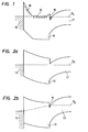
- Figure 1 shows the energy band diagram of the active region of this transistor. 13, 12, and 11 denote the gate electrode, the doped AlGaAs layer, and the substantially undoped GaAs layer, respectively.
- E designates the Fermi level.
- This figure illustrates the state where the carriers which are denoted by 15 are confined in a two-dimensional potential well parallel to the plane of the said interface.
- the carriers 15 are provided by the donor levels (14) in AlGaAs layer (12), and transit in undoped GaAs layer (11). Namely, the carriers are separated spacially from ionized donor impurities. Henceforth, the probability of the carrier scattering by ionized impurity potential will be decreased and as a result the mobility of the electrons becomes high.
- the transconductance becomes small, because the gate voltage is not effectively applied to the interface due to the highly added donors.
- a first object of this invention is to provide a semiconductor device with an enhanced electron mobility.
- Another object of this invention is to provide a semiconductor device containing transistors of both enhancement and depletion modes which can be fabricated in a simple procedure.
- the semiconductor device of the present invention comprises, at least, a heterojunction formed by a first semiconductor layer and a second semiconductor layer where the forbidden band gap of the said first semiconductor is smaller than that of the said second semiconductor, at least, one pair of electrode regions connected electronically to the said first semiconductor layer and a means to control the carrier density in the said first semiconductor layer where the impurities are not included substantially in the region in the first semiconductor under the means to control the carriers and are included in the region adjacent to the said one pair of electrodes.
- the density of the impurities in this region is preferably larger than 10 cm -3 .
- the semiconductor device of this invention has the following advantages with this structure.
- AlGaAs means Al x Ga 1-x As (0 ⁇ x ⁇ 1).
- the energy difference of the conduction band edges in GaAs and AlGaAs at the interface is ca.0.3 eV and the Schottky barrier height is ca.0.6 eV. Accordingly, when undoped AlGaAs is used, the conduction channel is not formed without applying gate voltage.
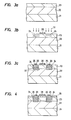
- Fig.2a shows the energy band structure for such cases.
- the symbols 13, 12, 11, and E F represent the gate electrode, the AlGaAs layer, GaAs layer, and the Fermi level, respectively.
- the transistor is in a normally-off state and the channel is formed by the application of the gate voltage. That is, it becomes possible to construct a transistor which operates in an enhancement mode.
- Fig.3c shows the cross-sectional structure of a. typical example of semiconductor devices of the present invention.
- the regions denoted by 21, 22, 23, 24, 25 and 26, 28, and 29 and 30 represent the GaAs substrate, a GaAs layer, the AlGaAs layer, the impurity-doped region adjacent to the electrode region, one pair of electrode regions, the control electrode (usually, gate electrode), and metal electrodes, respectively.
- One or more semiconductor layers can be formed between the semiconductor substrate 21 and the first semiconductor layer 22, whenever necessary. These semiconductor layers are formed conventionally in order to improve the crystalline quality of the first semiconductor layer.
- the impurity density in the semiconductor layer is smaller than approximately 10 cm -3 .
- 32 represents the carriers induced near the hetero-interface.
- the channel and the electrode regions (25,26) are favourably connected by these induced carriers.
- the first semiconductor layer 22 is a substantially non-doped GaAs layer with a thickness of 0.2 to 5 ⁇ m grown by molecular beam epitaxy method (MBE).
- the second semiconductor layer is a substantially non-doped AlGaAs layer with an energy gap larger than-that of GaAs by ca. 0.15 ⁇ 0.4 eV and with a thickness of 10 nm to 500 nm grown by MBE.
- the impurity-doped regions 24 adjacent to electrode regions are formed by masked ion implantation of donor impurities such as Si ions.
- donor impurities also germanium Ge, tin Sn, tellurium Te, selenium Se, sulfur S, etc. are applicable.
- the dose level of ion implantation is determined by the required characteristics of the device of the interest. In many cases, a dose level of ca. 10 13 to 10 14 cm -2 is used.
- the energy for ion implantation ranges from 50 to 200 keV depending upon the implant species.
- the specimen is annealed in an inert gas such as argon Ar and nitrogen N 2 kept at 500 to 850 C for 5 min. to 10 hours to activate the implanted species.
- the annealing temperature should not be too high, otherwise the AlGaAs-GaAs interface will be deteriorated.
- the source and drain electrode regions are formed by depositing, for example, Au-Ge alloy (200 nm)- Ni (10 nm)- Au-Ge alloy (300 nm) on the required portions and heating in a flowing hydrogen ambient of 400°C for 5 min.
- the carriers are induced in the channel region by applying a positive gate voltage with an appropriate magnitude.
- a positive gate voltage By applying an electric field between the source and drain electrodes, the electrons transit from the source region through the said region 24 adjacent to the source region where the carriers are induced due to ion implanted donors, the channel described above, and the said region 24 adjacent to the drain region and the drain electrode.
- This electric current is controled by the gate voltage. That is, this semiconductor device operates as a field-effect transistor.
- this invention was explained referring to a semiconductor device comprising a GaAs-AlGaAs system, this concept is applicable also to the hetero-junction systems comprising the combination of other materials such as Al y Ga 1-Y As-Al x Ga 1-x As, GaAs-Al x Ga 1-x As l-y Py, InP-In x Ga l-x AsyP 1-y , In P-In x Ga 1-x As, InAs-GaAs Sb 1-x' etc where 0 ⁇ x ⁇ 1 and 0 ⁇ y ⁇ 1.
- Al y Ga 1-Y As-Al x Ga 1-x As system it is preferable that 0 ⁇ x ⁇ 0.5, 0 ⁇ y ⁇ 0.5 and x ⁇ y.
- the transistors of the present invention are very favourably integrated. That is, in case there rises a need for integrating depletion mode transistors with those of enhancement mode operation, at first one fabricates enhancement mode transistors and implants donors into the AlGaAs regions under ;the gate electrodes for the transistors which should operate in depletion mode to the dose level that the transistors become normally-on type.
- a non-doped GaAs layer 22 with a thickness of about 1 ⁇ m (usually, 0.2 to 5 ⁇ m) is deposited at the substrate temperature of 580°C (usually 500 to 850°C) by conventional molecular beam epitaxy method (MBE), and thereupon an AlGaAs layer 23 with a thickness of 120 nm (usually, 10 to 500 nm) where the compositional ratio of Al vs Ga is about 0.3 : 0.7 is grown.
- MBE molecular beam epitaxy method
- a metal film for the gate electrode for example titanium Ti, with a thickness of ca. 2um is deposited upon the epitaxial layer above, and is patterned into the form of agate electrode with a width of 1.5 ⁇ m using a conventional photolithographic technique.
- silicon S i ions 31 are implanted with an acceleration energy of 70 keV to a dose level of 2 x 10 13 cm -2 (Fig.3b).
- annealing was performed at 750°C for 30 minutes. The portion denoted by 24 in Fig.3b is this impurity-doped region.
- the annealing at the temperature described above was adopted to prevent inter-diffusion at the GaAs-AlGaAs interface and diffusion of impurities.
- germanium Ge, tin Sn, tellulium Te, selenium Se, sulfur S, etc. can be used besides silicon mentioned above.
- the dose levels are determined depending on the requirements for the characteristics of the semiconductor device of interest.
- the energy for the implantation which varies depending on the implantation species ranges 50 ⁇ 200 keV.
- the source 25 and drain 26 electrodes are formed to be connected with the ion implanted regions by a conventional alloying method.
- metal Al electrodes 29, 30
- a field-effect transistor of the present invention is fabricated.
- 32 denotes the carriers induced at the interface.
- the source and drain electrode regions are formed by depositing Au-Ge alloy (200 nm) - Ni (10 nm) - Au-Ge alloy (300 nm) on the desired portions and heating in a hydrogen ambient at 400°C for 5 min.
- the field-effect transistor thus fabricated gave 1.5 times larger mobility and 3 times larger transconductance compared with a conventional hetero-junction transistor. having an AlGaAs layer doped with about 2 x 10 18 cm -3 donors.
- GaAs layer 35 which is more stable than AlGaAs upon the AlGaAs layer on top of the semiconductor assembly.
- the thickness of this GaAs film is favourably 20 to 200 nm.
- Fig.4 This example is shown in Fig.4 as a cross-sectional structure of the device.
- the GaAs layer 3 5 is formed on the AlGaAs layer 23 and protects the surface of the semiconductor assembly.
- Fig.3 and 4 denote the same portions.
- the present invention can be applied to materials other than the GaAs-AlGaAs system.
- the following will explain an embodiment using a semi-insulating InP substrate.
- the basic structure is the same as that shown in Figures 3a. ⁇ 3c.
- a 1 pm thick undoped In 0.53 Ga 0.47 As layer 22 and a 0.1 ⁇ m thick undoped In 0.40 Al 0.60 As layer 23 are epitaxially grown on a high-resistive InP substrate 21.
- donor impurities tin Sn is used besides silicon Si mentioned in the above embodiment.
- Aluminum is used for the gate electrode 28, while the source 25 and drain 26 electrodes are formed to be connected with the ion implanted regions by an Au-Ge alloying method. Then, aluminum metal electrodes (29, 30) are formed.
- a field-effect transistor of the present invention is fabricated.
- the carriers are induced at the interface between In 0.40 Al 0.60 As layer and In 0.53 Ga 0.47 As layer.
- III-V semiconductors such as InAs, GaP, GaSb etc.can be used in place of GaAs as substrate 21, and also other III-V semiconductors and semiconductor alloys as InAs, InSb, Al x Ga 1-x As, In x Ga 1-x As , In x Ga 1-x As y P 1-y , etc. can be used as the said first semiconductor layer and the said second semiconductor layer.
- the elementary construction of the integrated circuits comprises enhancement-mode and depletion-mode field-effect transistors. Explanation is made by refering to Fig.5a ⁇ Fig.5d.
- a GaAs layer 22 with a thickness of ca. 1 pm and an AlGaAs layer 23 with a thickness of about 120 nm are grown on the semi-insulating GaAs substrate 21 (Fig.5a).
- the GaAs layer 22 and the AlGaAs layer do not contain impurities effectively as in the case of Embodiment 1.
- silicon ions (24') are implanted .into the regions where depletion-mode transistors should be fabricated to a dose level of 2 x 10 13 cm -2 ( Fig.5b ).
- implantation of ions is preferably limited to the AlGaAs layer.
- the second ion implantation is made into the regions 27, 27' which should act as source and drain electrode regions of the transistor by using the gate electrodes formed above under the same conditions as in the case of Embodiment 1 and the same annealing is made (Fig. 5c).
- the range of the ions is preferably determined so as to be apart from the semiconductor hetero-junction by more than 30 nm in the direction of the gate electrodes and to leave an unimplanted buffer layer in the AlGaAs layer.
- the fabrication process after this stage is the same as in Embodiment 1. That is, the electrode regions 26, 25, 36 are formed with a usual alloy method to connect them with the ion implanted regions 27 and 24'. Further, by forming metal electrodes 28, 29, 30, 28' and 29, the field-effect transistors are completed (Fig.5d). In Fig.5d, the region denoted by 40 is the enhancement-mode transistor region and the region 41 is the depletion-mode transistor region.
- Futhermore as donor impurities described above, also germanium Ge, tin Sn, tellurium Te, selenium Se, sulfur S, etc. can be applied besides silicon Si.
- the dose level is determined by the required characteristics in the range 10 12 to 10 13 cm -2 .
- the acceleration energy for implantation depends upon the species implanted and is mostly in the range 50 to 200 keV.
- the source and drain regions may be formed by depositing, for example, Au-Ge alloy (200 nm) - Ni (10 nm) - Au-Ge alloy (300 nm) on the desired portions and annealing in a hydrogen ambient at 400°C for 5 min.
- the semiconductor devices are very favourably integrated. That is, both the enehancement-mode and the depletion-mode transistors are fabricated simultaneously by introducing impurities only into the regions where depletion-mode transistors are required with, for example, ion implantation and changing the shape of the potential well near the hetero-junction so as to shift the threshold gate voltage in the procedure to fabricate the enhancement-mode transistors of the present invention.
Landscapes
- Junction Field-Effect Transistors (AREA)
Applications Claiming Priority (2)
| Application Number | Priority Date | Filing Date | Title |
|---|---|---|---|
| JP189339/81 | 1981-11-27 | ||
| JP56189339A JPS5891682A (ja) | 1981-11-27 | 1981-11-27 | 半導体装置 |
Publications (3)
| Publication Number | Publication Date |
|---|---|
| EP0080714A2 true EP0080714A2 (fr) | 1983-06-08 |
| EP0080714A3 EP0080714A3 (en) | 1985-09-04 |
| EP0080714B1 EP0080714B1 (fr) | 1989-05-31 |
Family
ID=16239679
Family Applications (1)
| Application Number | Title | Priority Date | Filing Date |
|---|---|---|---|
| EP82110954A Expired EP0080714B1 (fr) | 1981-11-27 | 1982-11-26 | Dispositif semi-conducteur à hétéro-jonctions |
Country Status (5)
| Country | Link |
|---|---|
| US (1) | US4559547A (fr) |
| EP (1) | EP0080714B1 (fr) |
| JP (1) | JPS5891682A (fr) |
| CA (1) | CA1195436A (fr) |
| DE (1) | DE3279749D1 (fr) |
Cited By (5)
| Publication number | Priority date | Publication date | Assignee | Title |
|---|---|---|---|---|
| EP0146962A3 (fr) * | 1983-12-26 | 1985-10-30 | Hitachi, Ltd. | Dispositif semi-conducteur à structure à hétérojonctions |
| EP0131379A3 (en) * | 1983-06-09 | 1986-09-10 | Fujitsu Limited | Semiconductor device having a heterojunction, and method for producing it |
| FR2592739A1 (fr) * | 1986-01-06 | 1987-07-10 | Brillouet Francois | Structure semi-conductrice monolithique d'un laser et d'un transistor a effet de champ et son procede de fabrication |
| AU593086B2 (en) * | 1986-04-05 | 1990-02-01 | Sumitomo Electric Industries, Ltd. | Compound semiconductor device |
| DE102013218134A1 (de) | 2013-09-11 | 2015-03-12 | Evonik Industries Ag | Beschichtungsmittel enthaltend Polysiloxan-Quats |
Families Citing this family (10)
| Publication number | Priority date | Publication date | Assignee | Title |
|---|---|---|---|---|
| JPS59168677A (ja) * | 1983-03-14 | 1984-09-22 | Fujitsu Ltd | 半導体装置及びその製造方法 |
| JPS60239066A (ja) * | 1984-05-11 | 1985-11-27 | Hitachi Ltd | 半導体装置 |
| NL8500218A (nl) * | 1985-01-28 | 1986-08-18 | Philips Nv | Halfgeleiderinrichting met tweedimensionaal ladingsdragergas. |
| US4652896A (en) * | 1985-06-27 | 1987-03-24 | The United States Of America As Represented By The Secretary Of The Air Force | Modulation doped GaAs/AlGaAs field effect transistor |
| US4672414A (en) * | 1985-06-28 | 1987-06-09 | Texas Instruments Incorporated | Planar heterojunction bipolar device and method |
| USH411H (en) | 1985-08-28 | 1988-01-05 | United States Of America | Quasi-accumulation mode FET |
| US4903092A (en) * | 1986-08-12 | 1990-02-20 | American Telephone And Telegraph Company, At&T Bell Laboratories | Real space electron transfer device using hot electron injection |
| EP0622834A3 (fr) * | 1993-04-30 | 1998-02-11 | International Business Machines Corporation | Méthode pour prévenir le latch-up et améliorer la tension de claquage dans les MOSFET SOI |
| KR0137601B1 (ko) * | 1994-09-16 | 1998-04-28 | 양승택 | 전자의 간섭성을 이용한 양자간섭 트랜지스터 |
| JP4744109B2 (ja) | 2004-07-20 | 2011-08-10 | トヨタ自動車株式会社 | 半導体装置とその製造方法 |
Family Cites Families (7)
| Publication number | Priority date | Publication date | Assignee | Title |
|---|---|---|---|---|
| US4157556A (en) * | 1977-01-06 | 1979-06-05 | Varian Associates, Inc. | Heterojunction confinement field effect transistor |
| US4163237A (en) * | 1978-04-24 | 1979-07-31 | Bell Telephone Laboratories, Incorporated | High mobility multilayered heterojunction devices employing modulated doping |
| FR2465317A2 (fr) * | 1979-03-28 | 1981-03-20 | Thomson Csf | Transistor a effet de champ a frequence de coupure elevee |
| DE2913068A1 (de) * | 1979-04-02 | 1980-10-23 | Max Planck Gesellschaft | Heterostruktur-halbleiterkoerper und verwendung hierfuer |
| US4236166A (en) * | 1979-07-05 | 1980-11-25 | Bell Telephone Laboratories, Incorporated | Vertical field effect transistor |
| FR2465318A1 (fr) * | 1979-09-10 | 1981-03-20 | Thomson Csf | Transistor a effet de champ a frequence de coupure elevee |
| CA1145482A (fr) * | 1979-12-28 | 1983-04-26 | Takashi Mimura | Dispositif a semiconducteur a heterojonction unique a grande mobilite electronique |
-
1981
- 1981-11-27 JP JP56189339A patent/JPS5891682A/ja active Granted
-
1982
- 1982-11-24 US US06/444,233 patent/US4559547A/en not_active Expired - Lifetime
- 1982-11-26 CA CA000416463A patent/CA1195436A/fr not_active Expired
- 1982-11-26 EP EP82110954A patent/EP0080714B1/fr not_active Expired
- 1982-11-26 DE DE8282110954T patent/DE3279749D1/de not_active Expired
Cited By (10)
| Publication number | Priority date | Publication date | Assignee | Title |
|---|---|---|---|---|
| EP0131379A3 (en) * | 1983-06-09 | 1986-09-10 | Fujitsu Limited | Semiconductor device having a heterojunction, and method for producing it |
| US4795717A (en) * | 1983-06-09 | 1989-01-03 | Fujitsu Limited | Method for producing semiconductor device |
| EP0146962A3 (fr) * | 1983-12-26 | 1985-10-30 | Hitachi, Ltd. | Dispositif semi-conducteur à structure à hétérojonctions |
| FR2592739A1 (fr) * | 1986-01-06 | 1987-07-10 | Brillouet Francois | Structure semi-conductrice monolithique d'un laser et d'un transistor a effet de champ et son procede de fabrication |
| EP0232662A1 (fr) * | 1986-01-06 | 1987-08-19 | François Brillouet | Structure semi-conductrice monolithique d'un laser et d'un transistor à effet de champ et son procédé de fabrication |
| US4766472A (en) * | 1986-01-06 | 1988-08-23 | Francois Brillouet | Monolithic semiconductor structure of a laser and a field effect transistor |
| AU593086B2 (en) * | 1986-04-05 | 1990-02-01 | Sumitomo Electric Industries, Ltd. | Compound semiconductor device |
| DE102013218134A1 (de) | 2013-09-11 | 2015-03-12 | Evonik Industries Ag | Beschichtungsmittel enthaltend Polysiloxan-Quats |
| EP2848664A1 (fr) | 2013-09-11 | 2015-03-18 | Evonik Industries AG | Agent de revêtement contenant des composés d'ammonium quaternaire de polysiloxane |
| US9353289B2 (en) | 2013-09-11 | 2016-05-31 | Evonik Degussa Gmbh | Coating composition comprising polysiloxane quats |
Also Published As
| Publication number | Publication date |
|---|---|
| EP0080714B1 (fr) | 1989-05-31 |
| DE3279749D1 (en) | 1989-07-06 |
| JPS5891682A (ja) | 1983-05-31 |
| EP0080714A3 (en) | 1985-09-04 |
| CA1195436A (fr) | 1985-10-15 |
| JPH0324782B2 (fr) | 1991-04-04 |
| US4559547A (en) | 1985-12-17 |
Similar Documents
| Publication | Publication Date | Title |
|---|---|---|
| EP0114962A2 (fr) | Transistor à effet de champ à double hétérojonction | |
| EP0067721B1 (fr) | Dispositif semiconducteur à hétérojonctions | |
| US4452646A (en) | Method of making planar III-V compound device by ion implantation | |
| US4559547A (en) | Semiconductor device | |
| US7187045B2 (en) | Junction field effect metal oxide compound semiconductor integrated transistor devices | |
| EP0051271B1 (fr) | Dispositif semiconducteur à hétérojonctions | |
| EP0130676B1 (fr) | Dispositif semi-conducteur ayant une hétéro-jonction | |
| US4673959A (en) | Heterojunction FET with doubly-doped channel | |
| US5192698A (en) | Making staggered complementary heterostructure FET | |
| US4866491A (en) | Heterojunction field effect transistor having gate threshold voltage capability | |
| US5381027A (en) | Semiconductor device having a heterojunction and a two dimensional gas as an active layer | |
| US5258631A (en) | Semiconductor device having a two-dimensional electron gas as an active layer | |
| KR910006698B1 (ko) | 반도체 장치 | |
| EP0437702B1 (fr) | Circuit integré à semi-conducteurs comportant des régions d'isolation entre les composants formés de semi-conducteurs composés et méthode pour sa fabrication | |
| EP0146962A2 (fr) | Dispositif semi-conducteur à structure à hétérojonctions | |
| EP0278110B1 (fr) | Transistor à effet de champ à hétérojonction | |
| JPH0513462A (ja) | 化合物半導体構造 | |
| JPH01183164A (ja) | 高電子移動度電界効果型トランジスタ | |
| JPS60263476A (ja) | 半導体装置の製法 | |
| JPS63219176A (ja) | 電界効果トランジスタの製造方法 | |
| JPH04207040A (ja) | 半導体装置 | |
| JPH04233241A (ja) | 高耐圧電界効果トランジスタ | |
| GB2069754A (en) | Field effect transistor | |
| JPS6251268A (ja) | 半導体装置 | |
| JPS6143443A (ja) | 半導体装置の製造方法 |
Legal Events
| Date | Code | Title | Description |
|---|---|---|---|
| PUAI | Public reference made under article 153(3) epc to a published international application that has entered the european phase |
Free format text: ORIGINAL CODE: 0009012 |
|
| AK | Designated contracting states |
Designated state(s): DE FR GB NL |
|
| 17P | Request for examination filed |
Effective date: 19841220 |
|
| PUAL | Search report despatched |
Free format text: ORIGINAL CODE: 0009013 |
|
| AK | Designated contracting states |
Designated state(s): DE FR GB NL |
|
| 17Q | First examination report despatched |
Effective date: 19870915 |
|
| GRAA | (expected) grant |
Free format text: ORIGINAL CODE: 0009210 |
|
| AK | Designated contracting states |
Kind code of ref document: B1 Designated state(s): DE FR GB NL |
|
| PG25 | Lapsed in a contracting state [announced via postgrant information from national office to epo] |
Ref country code: NL Effective date: 19890531 |
|
| REF | Corresponds to: |
Ref document number: 3279749 Country of ref document: DE Date of ref document: 19890706 |
|
| ET | Fr: translation filed | ||
| NLV1 | Nl: lapsed or annulled due to failure to fulfill the requirements of art. 29p and 29m of the patents act | ||
| PLBE | No opposition filed within time limit |
Free format text: ORIGINAL CODE: 0009261 |
|
| STAA | Information on the status of an ep patent application or granted ep patent |
Free format text: STATUS: NO OPPOSITION FILED WITHIN TIME LIMIT |
|
| 26N | No opposition filed | ||
| PGFP | Annual fee paid to national office [announced via postgrant information from national office to epo] |
Ref country code: GB Payment date: 19961115 Year of fee payment: 15 Ref country code: FR Payment date: 19961115 Year of fee payment: 15 |
|
| PGFP | Annual fee paid to national office [announced via postgrant information from national office to epo] |
Ref country code: DE Payment date: 19970127 Year of fee payment: 15 |
|
| PG25 | Lapsed in a contracting state [announced via postgrant information from national office to epo] |
Ref country code: GB Free format text: LAPSE BECAUSE OF NON-PAYMENT OF DUE FEES Effective date: 19971126 |
|
| PG25 | Lapsed in a contracting state [announced via postgrant information from national office to epo] |
Ref country code: FR Free format text: THE PATENT HAS BEEN ANNULLED BY A DECISION OF A NATIONAL AUTHORITY Effective date: 19971130 |
|
| GBPC | Gb: european patent ceased through non-payment of renewal fee |
Effective date: 19971126 |
|
| PG25 | Lapsed in a contracting state [announced via postgrant information from national office to epo] |
Ref country code: DE Free format text: LAPSE BECAUSE OF NON-PAYMENT OF DUE FEES Effective date: 19980801 |
|
| REG | Reference to a national code |
Ref country code: FR Ref legal event code: ST |