EP0083253A2 - Appareil optique d'impression à cristaux liquides - Google Patents
Appareil optique d'impression à cristaux liquides Download PDFInfo
- Publication number
- EP0083253A2 EP0083253A2 EP82307039A EP82307039A EP0083253A2 EP 0083253 A2 EP0083253 A2 EP 0083253A2 EP 82307039 A EP82307039 A EP 82307039A EP 82307039 A EP82307039 A EP 82307039A EP 0083253 A2 EP0083253 A2 EP 0083253A2
- Authority
- EP
- European Patent Office
- Prior art keywords
- liquid crystal
- light
- crystal panel
- printing apparatus
- substrates
- Prior art date
- Legal status (The legal status is an assumption and is not a legal conclusion. Google has not performed a legal analysis and makes no representation as to the accuracy of the status listed.)
- Withdrawn
Links
Images






Classifications
-
- G—PHYSICS
- G06—COMPUTING OR CALCULATING; COUNTING
- G06K—GRAPHICAL DATA READING; PRESENTATION OF DATA; RECORD CARRIERS; HANDLING RECORD CARRIERS
- G06K15/00—Arrangements for producing a permanent visual presentation of the output data, e.g. computer output printers
- G06K15/02—Arrangements for producing a permanent visual presentation of the output data, e.g. computer output printers using printers
- G06K15/12—Arrangements for producing a permanent visual presentation of the output data, e.g. computer output printers using printers by photographic printing, e.g. by laser printers
- G06K15/1238—Arrangements for producing a permanent visual presentation of the output data, e.g. computer output printers using printers by photographic printing, e.g. by laser printers simultaneously exposing more than one point
- G06K15/1242—Arrangements for producing a permanent visual presentation of the output data, e.g. computer output printers using printers by photographic printing, e.g. by laser printers simultaneously exposing more than one point on one main scanning line
- G06K15/1252—Arrangements for producing a permanent visual presentation of the output data, e.g. computer output printers using printers by photographic printing, e.g. by laser printers simultaneously exposing more than one point on one main scanning line using an array of light modulators, e.g. a linear array
-
- B—PERFORMING OPERATIONS; TRANSPORTING
- B41—PRINTING; LINING MACHINES; TYPEWRITERS; STAMPS
- B41J—TYPEWRITERS; SELECTIVE PRINTING MECHANISMS, i.e. MECHANISMS PRINTING OTHERWISE THAN FROM A FORME; CORRECTION OF TYPOGRAPHICAL ERRORS
- B41J2/00—Typewriters or selective printing mechanisms characterised by the printing or marking process for which they are designed
- B41J2/435—Typewriters or selective printing mechanisms characterised by the printing or marking process for which they are designed characterised by selective application of radiation to a printing material or impression-transfer material
- B41J2/465—Typewriters or selective printing mechanisms characterised by the printing or marking process for which they are designed characterised by selective application of radiation to a printing material or impression-transfer material using masks, e.g. light-switching masks
-
- G—PHYSICS
- G02—OPTICS
- G02F—OPTICAL DEVICES OR ARRANGEMENTS FOR THE CONTROL OF LIGHT BY MODIFICATION OF THE OPTICAL PROPERTIES OF THE MEDIA OF THE ELEMENTS INVOLVED THEREIN; NON-LINEAR OPTICS; FREQUENCY-CHANGING OF LIGHT; OPTICAL LOGIC ELEMENTS; OPTICAL ANALOGUE/DIGITAL CONVERTERS
- G02F1/00—Devices or arrangements for the control of the intensity, colour, phase, polarisation or direction of light arriving from an independent light source, e.g. switching, gating or modulating; Non-linear optics
- G02F1/01—Devices or arrangements for the control of the intensity, colour, phase, polarisation or direction of light arriving from an independent light source, e.g. switching, gating or modulating; Non-linear optics for the control of the intensity, phase, polarisation or colour
- G02F1/13—Devices or arrangements for the control of the intensity, colour, phase, polarisation or direction of light arriving from an independent light source, e.g. switching, gating or modulating; Non-linear optics for the control of the intensity, phase, polarisation or colour based on liquid crystals, e.g. single liquid crystal display cells
- G02F1/133—Constructional arrangements; Operation of liquid crystal cells; Circuit arrangements
-
- G—PHYSICS
- G02—OPTICS
- G02F—OPTICAL DEVICES OR ARRANGEMENTS FOR THE CONTROL OF LIGHT BY MODIFICATION OF THE OPTICAL PROPERTIES OF THE MEDIA OF THE ELEMENTS INVOLVED THEREIN; NON-LINEAR OPTICS; FREQUENCY-CHANGING OF LIGHT; OPTICAL LOGIC ELEMENTS; OPTICAL ANALOGUE/DIGITAL CONVERTERS
- G02F1/00—Devices or arrangements for the control of the intensity, colour, phase, polarisation or direction of light arriving from an independent light source, e.g. switching, gating or modulating; Non-linear optics
- G02F1/01—Devices or arrangements for the control of the intensity, colour, phase, polarisation or direction of light arriving from an independent light source, e.g. switching, gating or modulating; Non-linear optics for the control of the intensity, phase, polarisation or colour
- G02F1/13—Devices or arrangements for the control of the intensity, colour, phase, polarisation or direction of light arriving from an independent light source, e.g. switching, gating or modulating; Non-linear optics for the control of the intensity, phase, polarisation or colour based on liquid crystals, e.g. single liquid crystal display cells
- G02F1/133—Constructional arrangements; Operation of liquid crystal cells; Circuit arrangements
- G02F1/1333—Constructional arrangements; Manufacturing methods
- G02F1/1335—Structural association of cells with optical devices, e.g. polarisers or reflectors
-
- G—PHYSICS
- G02—OPTICS
- G02F—OPTICAL DEVICES OR ARRANGEMENTS FOR THE CONTROL OF LIGHT BY MODIFICATION OF THE OPTICAL PROPERTIES OF THE MEDIA OF THE ELEMENTS INVOLVED THEREIN; NON-LINEAR OPTICS; FREQUENCY-CHANGING OF LIGHT; OPTICAL LOGIC ELEMENTS; OPTICAL ANALOGUE/DIGITAL CONVERTERS
- G02F1/00—Devices or arrangements for the control of the intensity, colour, phase, polarisation or direction of light arriving from an independent light source, e.g. switching, gating or modulating; Non-linear optics
- G02F1/01—Devices or arrangements for the control of the intensity, colour, phase, polarisation or direction of light arriving from an independent light source, e.g. switching, gating or modulating; Non-linear optics for the control of the intensity, phase, polarisation or colour
- G02F1/13—Devices or arrangements for the control of the intensity, colour, phase, polarisation or direction of light arriving from an independent light source, e.g. switching, gating or modulating; Non-linear optics for the control of the intensity, phase, polarisation or colour based on liquid crystals, e.g. single liquid crystal display cells
- G02F1/137—Devices or arrangements for the control of the intensity, colour, phase, polarisation or direction of light arriving from an independent light source, e.g. switching, gating or modulating; Non-linear optics for the control of the intensity, phase, polarisation or colour based on liquid crystals, e.g. single liquid crystal display cells characterised by the electro-optical or magneto-optical effect, e.g. field-induced phase transition, orientation effect, guest-host interaction or dynamic scattering
- G02F1/139—Devices or arrangements for the control of the intensity, colour, phase, polarisation or direction of light arriving from an independent light source, e.g. switching, gating or modulating; Non-linear optics for the control of the intensity, phase, polarisation or colour based on liquid crystals, e.g. single liquid crystal display cells characterised by the electro-optical or magneto-optical effect, e.g. field-induced phase transition, orientation effect, guest-host interaction or dynamic scattering based on orientation effects in which the liquid crystal remains transparent
- G02F1/1392—Devices or arrangements for the control of the intensity, colour, phase, polarisation or direction of light arriving from an independent light source, e.g. switching, gating or modulating; Non-linear optics for the control of the intensity, phase, polarisation or colour based on liquid crystals, e.g. single liquid crystal display cells characterised by the electro-optical or magneto-optical effect, e.g. field-induced phase transition, orientation effect, guest-host interaction or dynamic scattering based on orientation effects in which the liquid crystal remains transparent using a field-induced sign-reversal of the dielectric anisotropy
Definitions
- the fibres may be joined into a unitary array.
- Light may be allowed to pass through said liquid crystal panel when said liquid crystal molecules are oriented paralled to said substrates, light being prevented from passing through said liquid crystal panel when said liquid crystal molecules are oriented perpendicularly to said substrates.
- the developed toner image is then transferred by a transfer corona discharge unit onto a sheet D of recording paper travelling in synchronism with the photosensitive drum B by virtue of being passed between the latter and a roller E.
- the toner image is fixed to the sheet D by a fixing unit F with light, heat and pressure applied thereby.
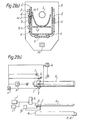
- a light source k such as a tungsten lamp, a halogen lamp, a xenon lamp, or a fluorescent lamp, emits light which travels through a light outlet or slit defined in a light shield or shield plate o and irradiates the liquid crystal panel a.
- the light shield o other than at the light outlet, blocks the light and heat emitted from the light source k.
- a signal electrode a-13 formed on the lower substrate a-4 is indicated by solid lines, while a scanning elelctrode a-12 formed on the upper substrate a-3 is indicated by dotted lines.
- the electrical resistance from the drivers b .(Fig. 2) to the liquid crystal material a-2 can be reduced and thus the time constant can be lowered.
- the lowered time constant is particularly important for the printing apparatus A of the invention in which the liquid crystal panel is driven at a high frequency for high-speed response.
- a liquid crystal panel a which was thus constructed had a low relaxation frequency of 5 KHz at 25 0 C, and thus could be driven with ease with low power consumption.
- the dielectric anisotropy at a low frequency was large as it was 6 at 500 Hz and 5 at a higher frequency of 7 0 K H z, a value sufficient for controlling the orientation of the molecules of the liquid crystal material a-2.
- the viscosity of the liquid crystal molecules was low, it being about 10 CPS. When driven at a high frequency of 70 KHz, the liquid crystal material exhibited a sufficiently high response.
- the liquid crystal panel a of the above structure was excellent in its ability to resist environmental attack and aging. For example, the molecule orientation and current consumption requirement were not changed when the liquid crystal panel was left for one month at 60°C and 90% RH (relative humidity). No problem occurred after the liquid crystal panel had been left in an atmosphere of 80°C for three months.
- the liquid crystal panel a described above is completely different from conventional liquid crystal panels of the DSM type, and is suitable for practical use from the standpoints of reliability and aging.
- Prior liquid crystal display panels of the DSM type lacked sufficient reliability because a dopant is added to the liquid crystal material for optical dispersion, and this consumed a large amount of current. Threrefore, such conventional LCD panels failed to find widespread use.
- the use of a liquid crystal material as described above of a twisted nematic-structure ensures a greatly improved reliability and current consumption.
- the printing apparatus of the present invention is thus able to effect high-speed printing by maintaining the liquid crystal panel a at a constant temperature.
- Fig. 5(b) also shows a signal S 1 for driving the signal electrodes a-13.
- a composite signal waveform COM-1 S 1 is applied to the liquid crystal at the crossing of the scanning electrode COM-1 and the signal electrode to which the signal S 1 is applied, and a composite signal waveform COM-2 S 1 is applied to the liquid crystal at the crossing of the scanning electrode a-12 COM-2 and the signal electrode a-13 to which the signal S 1 is applied.
- Fig. 5(b) also shows a signal S 2 for driving the signal electrodes a-13.
- a composite signal waveform COM-1 S 2 is applied to the liquid crystal at the crossing of the scanning electrode a-12 COM-1 and the signal electrode a-13 to which the signal S 2 is applied, and a composite signal waveform COM-2 S 2 is applied to the liquid crystal at the crossing of the scanning electrode a-12 COM-2 and the signal electrode a-13 to which the signal S 2 is applied.
- the peak value V 1 is in the range of from a few volts to a few tens of volts.
- a prototype of the apparatus according to the present invention was designed to be driven by signals having a peak value V 1 of 30V.
- the low-frequency signal had a frequency of a few hundreds Hz
- the high-frequency signal had a frequency of from a few tens to a few hundreds KHz.
- the frequency in the prototype was 130 KHz.
- the liquid crystal panel operates in the rise and fall times of 0.1 to 0.5 ms and the period T 1 is a few ms.
- the period T 1 was 2 ms in the prototype.
- the number of power supply levels in the power supply may only be two by equalizing high- and low-frequency voltages as in the embodiment of the present invention.
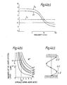
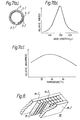
- Fig. 7(b) is a graph which shows a wavelength characteristic of a fluorescent material k-4 used in an Example according to the present invention, the graph having an ordinate representative of relative energy of the fluorescent material k-4 and an abscissa representative of wavelengths.
- the fluorescent material should have wavelengths matching those of a photosensitive material on the photosensitive drum B (Fig. 1), relative light discharge enery in a certain wavelength range, a reduced half-valve width, a high brightness, and a high longevity, the preferred material used being BaMgAll1014FeMu.
- the fluorescent material may have several wavelength peaks one of which is highest and sensed by the photosensitive material of the photosensitive drum B (Fig. 1), the others being negligible.
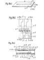
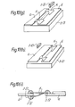
- the substrate d passes through the preheater z-12 which preheats the substrate d to a temperature ranging from 130 C to 200°C, and then is heated by the far-infrared heater z-13 which irradiates the substrate d with far-infrared radiation to melt the solder in the solder creams z-6 at a high temperature of more than 200 0 C for thereby soldering the ICs b to the substrate d.
- liquid crystal panel a and the driver substrate d are soldered to each other through the flexible substrates x for electrical and mechanical connection.
- Fig. 10(i) shows soldered junctions z-52 of the driver substrate d, and shows the flexible substrates x and liquid crystal panel a which are assembled together, the junctions z-52 being coated with reinforcing agents z-51 which may be composed of epoxy adhesive, urethaneadhesive, silicone adhesive or the like.
- the reinforcing agents z-51 cover portions of both the flexible substrates x and the driver substrate d at the junctions z-52 therebetween.
- the reinforcing agents z-51 also cover portions of both of the liquid crystal panel a and the flexible substrates x at the junctions therebetween.
Landscapes
- Physics & Mathematics (AREA)
- Nonlinear Science (AREA)
- Optics & Photonics (AREA)
- General Physics & Mathematics (AREA)
- Chemical & Material Sciences (AREA)
- Crystallography & Structural Chemistry (AREA)
- Engineering & Computer Science (AREA)
- Mathematical Physics (AREA)
- General Engineering & Computer Science (AREA)
- Theoretical Computer Science (AREA)
- Liquid Crystal (AREA)
- Printers Or Recording Devices Using Electromagnetic And Radiation Means (AREA)
Applications Claiming Priority (2)
| Application Number | Priority Date | Filing Date | Title |
|---|---|---|---|
| JP56213263A JPS58114978A (ja) | 1981-12-28 | 1981-12-28 | 液晶光学的印写装置 |
| JP213263/81 | 1981-12-28 |
Publications (2)
| Publication Number | Publication Date |
|---|---|
| EP0083253A2 true EP0083253A2 (fr) | 1983-07-06 |
| EP0083253A3 EP0083253A3 (fr) | 1985-10-23 |
Family
ID=16636195
Family Applications (1)
| Application Number | Title | Priority Date | Filing Date |
|---|---|---|---|
| EP82307039A Withdrawn EP0083253A3 (fr) | 1981-12-28 | 1982-12-22 | Appareil optique d'impression à cristaux liquides |
Country Status (3)
| Country | Link |
|---|---|
| US (2) | US4589732A (fr) |
| EP (1) | EP0083253A3 (fr) |
| JP (1) | JPS58114978A (fr) |
Cited By (8)
| Publication number | Priority date | Publication date | Assignee | Title |
|---|---|---|---|---|
| GB2139773A (en) * | 1983-03-15 | 1984-11-14 | Canon Kk | Multi-mode copier |
| FR2549614A1 (fr) * | 1983-07-22 | 1985-01-25 | Casio Computer Co Ltd | Appareil de formation d'image |
| GB2159315A (en) * | 1984-04-26 | 1985-11-27 | Canon Kk | Electrophotographic printers |
| GB2159655A (en) * | 1984-04-25 | 1985-12-04 | Canon Kk | Lcd matrix arrangements |
| EP0169518A3 (en) * | 1984-07-27 | 1987-07-22 | Casio Computer Company Limited | Liquid crystal apparatus |
| EP0239766A1 (fr) * | 1986-02-28 | 1987-10-07 | Siemens Aktiengesellschaft | Dispositif de contact pour un élément de visualisation, en particulier à cristaux liquides |
| US4729639A (en) * | 1982-03-29 | 1988-03-08 | Tektronix, Inc. | Dual frequency addressable liquid crystals and methods of use |
| US4836654A (en) * | 1986-06-30 | 1989-06-06 | Casio Computer Co., Ltd. | Drive method for a dual-frequency, dielectric anisotropy liquid crystal optical device |
Families Citing this family (37)
| Publication number | Priority date | Publication date | Assignee | Title |
|---|---|---|---|---|
| JPS58114978A (ja) * | 1981-12-28 | 1983-07-08 | Seiko Epson Corp | 液晶光学的印写装置 |
| JPS6041022A (ja) * | 1983-08-15 | 1985-03-04 | Seiko Epson Corp | 印写装置 |
| JPS60172131U (ja) * | 1984-04-20 | 1985-11-14 | ホシデン株式会社 | カラ−液晶表示器 |
| JPS6117127A (ja) * | 1984-07-04 | 1986-01-25 | Hitachi Ltd | 光スイツチ素子の駆動方法 |
| GB2163564A (en) * | 1984-08-25 | 1986-02-26 | Stc Plc | Thermal image sensor |
| US4838657A (en) * | 1984-11-15 | 1989-06-13 | Seiko Epson Corporation | Liquid crystal shutter |
| JPS61191083A (ja) * | 1985-02-20 | 1986-08-25 | Canon Inc | 画像記録装置 |
| GB8508280D0 (en) * | 1985-03-29 | 1985-05-09 | British Telecomm | Optical component mounting |
| US4915500A (en) * | 1985-08-16 | 1990-04-10 | The United States Of America As Represented By The Department Of Energy | Multichannel optical sensing device |
| JPS62165892A (ja) * | 1986-01-17 | 1987-07-22 | 株式会社東芝 | 温度検出装置 |
| US5047789A (en) * | 1986-02-20 | 1991-09-10 | Fuji Photo Film Co., Ltd. | Method for driving and controlling liquid crystal and device therefor |
| DE3750527T2 (de) * | 1986-06-30 | 1995-02-23 | Casio Computer Co Ltd | Flüssigkristallvorrichtung und ihre Verwendung in optischen Druckern. |
| US4837097A (en) * | 1987-12-17 | 1989-06-06 | Xerox Corporation | Optical Shield for liquid crystal devices and method of fabrication |
| US5293262A (en) * | 1988-03-15 | 1994-03-08 | Mitsubishi Denki Kabushiki Kaisha | Liquid crystal display device having heat-insulating members and driving circuit boards attached to rear edges of light box |
| US5054891A (en) * | 1988-04-15 | 1991-10-08 | Casio Computer Co., Ltd. | Liquid crystal shutter with substrates having an optical anisotropy caused by temperature gradient |
| US4921316A (en) * | 1989-03-06 | 1990-05-01 | Polaroid Corporation | Integral fiber optic printhead |
| US4974928A (en) * | 1989-04-03 | 1990-12-04 | Polaroid Corporation | Integral fiber optic printhead |
| JPH02287527A (ja) * | 1989-04-28 | 1990-11-27 | Fuji Photo Film Co Ltd | ビデオプリンタ |
| EP0425287B1 (fr) * | 1989-10-27 | 1995-09-20 | Nippon Paint Co., Ltd. | Procédé pour l'enregistrement de l'image et structure de film à cet effet |
| DE3937736A1 (de) * | 1989-11-13 | 1991-05-16 | Standard Elektrik Lorenz Ag | Elektrooptische schreibeinrichtung |
| US5150239A (en) * | 1990-02-09 | 1992-09-22 | Canon Kabushiki Kaisha | One-pack type epoxy sealant with amine-type curing agent, for liquid crystal cell, display apparatus and recording apparatus |
| KR910016199A (ko) * | 1990-02-27 | 1991-09-30 | 이헌조 | 비데오 프린터의 결상장치 |
| JP3158667B2 (ja) * | 1991-08-01 | 2001-04-23 | セイコーエプソン株式会社 | 液晶表示素子の製造方法及び液晶表示素子の再生方法 |
| US5246179A (en) * | 1991-08-23 | 1993-09-21 | Eastman Kodak Company | Optical fiber take-up assembly |
| JP2863982B2 (ja) * | 1994-01-25 | 1999-03-03 | 株式会社タイテック | ディスプレイスイッチ |
| JPH07253621A (ja) * | 1994-03-16 | 1995-10-03 | Fujitsu Ltd | スクリーン及びこれを用いた投写型表示装置 |
| EP0976008B1 (fr) * | 1997-04-14 | 2003-01-22 | Dicon A/S | Appareil et procede d'eclairage d'un milieu photosensible |
| JP3410667B2 (ja) * | 1997-11-25 | 2003-05-26 | シャープ株式会社 | 反射型液晶表示装置およびその製造方法 |
| US6366338B1 (en) * | 1997-12-22 | 2002-04-02 | Citizen Watch Co. Ltd. | Line-scanning optical printer |
| ATE243616T1 (de) * | 1998-10-12 | 2003-07-15 | Dicon As | Rapid-prototyping-vorrichtung und rapid- prototyping-methode |
| WO2000069631A1 (fr) * | 1999-05-17 | 2000-11-23 | Creoscitex Corporation Ltd. | Photocomposeuse pleine page numerique dotee d'un micro-ecran haute resolution |
| JP3795734B2 (ja) * | 2000-08-25 | 2006-07-12 | 三菱電機株式会社 | 液晶制御装置 |
| KR100385066B1 (ko) * | 2001-10-16 | 2003-05-23 | 삼성전자주식회사 | 레이저 스캐닝 유니트 |
| JP3863468B2 (ja) * | 2002-01-18 | 2006-12-27 | ローム株式会社 | プリントヘッドおよび画像形成装置 |
| JP3866670B2 (ja) * | 2003-03-05 | 2007-01-10 | ローム株式会社 | 液晶シャッタおよびプリントヘッド |
| US20090256900A1 (en) * | 2008-04-11 | 2009-10-15 | Dell Products L.P. | System and Method for Optical Printing on a Laser Printer |
| JP5874619B2 (ja) * | 2012-12-10 | 2016-03-02 | コニカミノルタ株式会社 | 光プリントヘッド、及び画像形成装置 |
Family Cites Families (36)
| Publication number | Priority date | Publication date | Assignee | Title |
|---|---|---|---|---|
| US2765458A (en) * | 1955-09-06 | 1956-10-02 | Ncr Co | Luminous rod read-out device |
| US3036153A (en) * | 1960-09-02 | 1962-05-22 | Gulton Ind Inc | Electro-optical scanning system |
| DE1288902B (de) * | 1966-09-10 | 1969-02-06 | Agfa Gevaert Ag | Verfahren und Vorrichtung zum optischen Kopieren von transparenten Vorlagen |
| US3622226A (en) * | 1969-11-19 | 1971-11-23 | Rca Corp | Liquid crystal cells in a linear array |
| US3621138A (en) * | 1969-12-17 | 1971-11-16 | Joseph T Mcnaney | Alphanumeric character recording apparatus |
| DE2041334C3 (de) * | 1970-08-20 | 1973-11-29 | Licentia Patent-Verwaltungs-Gmbh, 6000 Frankfurt | Zusatzeinrichtung fur die Aufzeich nung von Informationen von einem BiRl schirm |
| US4057338A (en) * | 1972-02-04 | 1977-11-08 | Izon Corporation | Fiber optic system |
| US3824604A (en) * | 1972-10-12 | 1974-07-16 | E Stein | Alphanumeric printing system employing liquid crystal matrix |
| DE2256966A1 (de) * | 1972-11-21 | 1974-05-22 | Basf Ag | Anordnung zum belichten von lichtempfindlichen materialien mit auf einem kathodenstrahlroehren-bildschirm dargestellten bildinformationen |
| DE2357721C3 (de) * | 1973-11-19 | 1979-02-22 | Hoechst Ag, 6000 Frankfurt | Anordnung für Beleuchtung und Abtastung in Projektionskopiereinrichtungen, insbesondere für elektrofotografische Kopiergeräte |
| JPS52123625A (en) * | 1976-04-09 | 1977-10-18 | Ricoh Co Ltd | Focusing optical system for electrophotographic copier |
| US4110794A (en) * | 1977-02-03 | 1978-08-29 | Static Systems Corporation | Electronic typewriter using a solid state display to print |
| US4194833A (en) * | 1977-02-03 | 1980-03-25 | Static Systems Corporation | Electronic typewriter having an electronic display |
| DE2711194A1 (de) * | 1977-03-15 | 1978-09-21 | Standard Elektrik Lorenz Ag | Vorrichtung zur belichtung einer auf einem bewegbaren traeger befindlichen fotoelektrischen schicht |
| US4190795A (en) * | 1977-09-09 | 1980-02-26 | Coberly & Associates | Constant intensity light source |
| JPS5489749A (en) * | 1977-12-27 | 1979-07-17 | Fuji Photo Optical Co Ltd | Lighting optical system of endoscope |
| JPS54136825A (en) * | 1978-04-15 | 1979-10-24 | Ricoh Co Ltd | Lighting device in imaging optical system |
| US4206501A (en) * | 1978-06-12 | 1980-06-03 | Motorola, Inc. | Apparatus and methods for back illuminating a display surface |
| JPS552254A (en) * | 1978-06-20 | 1980-01-09 | Ricoh Co Ltd | Focusing type optical transmission body array |
| FR2440667A1 (fr) * | 1978-10-31 | 1980-05-30 | Thomson Csf | Dispositif optique de reproduction d'images utilisant une cellule a cristal liquide et telecopieur comportant un tel dispositif |
| EP0022934A1 (fr) * | 1979-07-18 | 1981-01-28 | Siemens Aktiengesellschaft | Dispositif d'affichage électrooptique, en particulier affichage à cristal liquide |
| US4297022A (en) * | 1979-12-03 | 1981-10-27 | Static Systems Corporation | Light pipe valve liquid crystal transmissive display for direct imaging on photosensitive materials |
| US4386836A (en) * | 1979-12-28 | 1983-06-07 | Kabushiki Kaisha Suwa Seikosha | Electro-photographic printer |
| JPS56117217A (en) * | 1980-02-21 | 1981-09-14 | Sharp Corp | Liquid-crystal display recorder |
| US4349248A (en) * | 1980-04-23 | 1982-09-14 | Xerox Corporation | Gradient index lens array with improved exposure uniformity |
| US4373780A (en) * | 1980-06-16 | 1983-02-15 | Xerox Corporation | Image transmitting system utilizing a gradient index lens |
| US4331380A (en) * | 1980-05-21 | 1982-05-25 | Xerox Corporation | Gradient index lens array having reduction properties |
| JPS5714058A (en) * | 1980-06-28 | 1982-01-25 | Ricoh Co Ltd | Printer |
| US4364639A (en) * | 1980-08-25 | 1982-12-21 | Northern Telecom Limited | Variable attenuation electro-optic device |
| DE3140078A1 (de) * | 1980-10-08 | 1982-04-22 | Kabushiki Kaisha Suwa Seikosha, Tokyo | Optische fluessigkristalleinrichtung und drucker, der eine solche optische einrichtung als lichtventil benutzt |
| JPS57171378A (en) * | 1981-04-15 | 1982-10-21 | Suwa Seikosha Kk | Liquid crystal optical device |
| JPS57171881A (en) * | 1981-04-16 | 1982-10-22 | Nippon Sheet Glass Co Ltd | Display device |
| JPS5814127A (ja) * | 1981-07-16 | 1983-01-26 | Fuji Xerox Co Ltd | 複写機の照明装置 |
| JPS58114978A (ja) * | 1981-12-28 | 1983-07-08 | Seiko Epson Corp | 液晶光学的印写装置 |
| DE3224356A1 (de) * | 1982-06-30 | 1984-01-12 | Philips Patentverwaltung Gmbh, 2000 Hamburg | Optischer drucker mit lichtschaltelementen |
| US4727380A (en) * | 1984-05-31 | 1988-02-23 | Seiko Epson Corporation | Photosensitive printing apparatus |
-
1981
- 1981-12-28 JP JP56213263A patent/JPS58114978A/ja active Pending
-
1982
- 1982-12-22 EP EP82307039A patent/EP0083253A3/fr not_active Withdrawn
- 1982-12-23 US US06/452,370 patent/US4589732A/en not_active Expired - Lifetime
-
1986
- 1986-05-09 US US06/861,688 patent/US4859034A/en not_active Expired - Lifetime
Cited By (12)
| Publication number | Priority date | Publication date | Assignee | Title |
|---|---|---|---|---|
| US4729639A (en) * | 1982-03-29 | 1988-03-08 | Tektronix, Inc. | Dual frequency addressable liquid crystals and methods of use |
| GB2139773A (en) * | 1983-03-15 | 1984-11-14 | Canon Kk | Multi-mode copier |
| FR2549614A1 (fr) * | 1983-07-22 | 1985-01-25 | Casio Computer Co Ltd | Appareil de formation d'image |
| US4745433A (en) * | 1983-07-22 | 1988-05-17 | Casio Computer Co., Ltd. | Image forming apparatus with a light shutter of the G-H type liquid crystal |
| GB2159655A (en) * | 1984-04-25 | 1985-12-04 | Canon Kk | Lcd matrix arrangements |
| US4884079A (en) * | 1984-04-25 | 1989-11-28 | Canon Kabushiki Kaisha | Image forming apparatus and driving method therefor |
| GB2159315A (en) * | 1984-04-26 | 1985-11-27 | Canon Kk | Electrophotographic printers |
| EP0169518A3 (en) * | 1984-07-27 | 1987-07-22 | Casio Computer Company Limited | Liquid crystal apparatus |
| US4832460A (en) * | 1984-07-27 | 1989-05-23 | Casio Computer Co., Ltd. | Liquid crystal apparatus having pressure absorbing means |
| EP0239766A1 (fr) * | 1986-02-28 | 1987-10-07 | Siemens Aktiengesellschaft | Dispositif de contact pour un élément de visualisation, en particulier à cristaux liquides |
| US4836654A (en) * | 1986-06-30 | 1989-06-06 | Casio Computer Co., Ltd. | Drive method for a dual-frequency, dielectric anisotropy liquid crystal optical device |
| US4946260A (en) * | 1986-06-30 | 1990-08-07 | Casio Computer Co., Ltd. | Dual-frequency, dielectric anisotropy liquid crystal optical device |
Also Published As
| Publication number | Publication date |
|---|---|
| EP0083253A3 (fr) | 1985-10-23 |
| US4589732A (en) | 1986-05-20 |
| JPS58114978A (ja) | 1983-07-08 |
| US4859034A (en) | 1989-08-22 |
Similar Documents
| Publication | Publication Date | Title |
|---|---|---|
| EP0083253A2 (fr) | Appareil optique d'impression à cristaux liquides | |
| US4929057A (en) | Liquid crystal optical device | |
| US4810062A (en) | Liquid crystal cell with opaque mask for printing device | |
| GB2144869A (en) | Image forming apparatus | |
| EP0169518B1 (fr) | Dispositif à cristal liquide | |
| US4647156A (en) | Liquid crystal device | |
| GB2159315A (en) | Electrophotographic printers | |
| US5262888A (en) | Light shutter device | |
| US4763142A (en) | Electrophotographic printer with light micro-shutters | |
| KR900002679B1 (ko) | 액정광 셔터의 온도 제어장치 | |
| JPS6335002B2 (fr) | ||
| JPH0158488B2 (fr) | ||
| JPS60143315A (ja) | 液晶光スイツチアレイ | |
| JPS58193522A (ja) | 液晶光学的印写装置 | |
| JPS62153835A (ja) | 液晶素子 | |
| JP2576085B2 (ja) | 液晶素子 | |
| JPS58193517A (ja) | 液晶光学的印写装置 | |
| JPS6366979A (ja) | Ledアレイヘツド及びその製造方法 | |
| JPS61209415A (ja) | 光学的液体シヤツタ | |
| JPH0229355A (ja) | 画像記録装置 | |
| JPS60107371A (ja) | 光プリンタ | |
| JPS62153834A (ja) | 液晶素子 | |
| JPH09189888A (ja) | 光遮蔽装置及びそれを備えた情報伝達装置 | |
| JPH0546019Y2 (fr) | ||
| JPS62203125A (ja) | 液晶素子 |
Legal Events
| Date | Code | Title | Description |
|---|---|---|---|
| PUAI | Public reference made under article 153(3) epc to a published international application that has entered the european phase |
Free format text: ORIGINAL CODE: 0009012 |
|
| AK | Designated contracting states |
Designated state(s): DE FR GB IT |
|
| PUAL | Search report despatched |
Free format text: ORIGINAL CODE: 0009013 |
|
| RHK1 | Main classification (correction) |
Ipc: G02F 1/13 |
|
| AK | Designated contracting states |
Designated state(s): DE FR GB IT |
|
| RAP1 | Party data changed (applicant data changed or rights of an application transferred) |
Owner name: SEIKO EPSON CORPORATION |
|
| 17P | Request for examination filed |
Effective date: 19860416 |
|
| 17Q | First examination report despatched |
Effective date: 19870810 |
|
| STAA | Information on the status of an ep patent application or granted ep patent |
Free format text: STATUS: THE APPLICATION IS DEEMED TO BE WITHDRAWN |
|
| 18D | Application deemed to be withdrawn |
Effective date: 19871222 |
|
| RIN1 | Information on inventor provided before grant (corrected) |
Inventor name: SHIRAISHI, YOSHIAKI |