EP0083394B1 - Procédé et appareil pour l'illumination uniforme d'une surface - Google Patents
Procédé et appareil pour l'illumination uniforme d'une surface Download PDFInfo
- Publication number
- EP0083394B1 EP0083394B1 EP19820109182 EP82109182A EP0083394B1 EP 0083394 B1 EP0083394 B1 EP 0083394B1 EP 19820109182 EP19820109182 EP 19820109182 EP 82109182 A EP82109182 A EP 82109182A EP 0083394 B1 EP0083394 B1 EP 0083394B1
- Authority
- EP
- European Patent Office
- Prior art keywords
- area
- reflecting means
- mask
- source
- time
- Prior art date
- Legal status (The legal status is an assumption and is not a legal conclusion. Google has not performed a legal analysis and makes no representation as to the accuracy of the status listed.)
- Expired
Links
- 238000005286 illumination Methods 0.000 title claims description 29
- 238000000034 method Methods 0.000 title claims description 14
- 230000005855 radiation Effects 0.000 claims description 39
- 230000004907 flux Effects 0.000 claims description 15
- 230000033001 locomotion Effects 0.000 claims description 14
- 238000001459 lithography Methods 0.000 claims description 8
- 238000010438 heat treatment Methods 0.000 claims description 4
- 230000000737 periodic effect Effects 0.000 claims description 4
- 238000012887 quadratic function Methods 0.000 claims 1
- 238000009304 pastoral farming Methods 0.000 description 25
- 238000001015 X-ray lithography Methods 0.000 description 15
- 238000003860 storage Methods 0.000 description 11
- 230000008859 change Effects 0.000 description 9
- 238000009826 distribution Methods 0.000 description 9
- 238000002310 reflectometry Methods 0.000 description 8
- 238000010894 electron beam technology Methods 0.000 description 4
- 230000003595 spectral effect Effects 0.000 description 4
- 238000001228 spectrum Methods 0.000 description 4
- 230000005540 biological transmission Effects 0.000 description 3
- 238000010586 diagram Methods 0.000 description 3
- PCHJSUWPFVWCPO-UHFFFAOYSA-N gold Chemical compound [Au] PCHJSUWPFVWCPO-UHFFFAOYSA-N 0.000 description 3
- 239000010931 gold Substances 0.000 description 3
- 229910052737 gold Inorganic materials 0.000 description 3
- 230000003287 optical effect Effects 0.000 description 3
- 230000008569 process Effects 0.000 description 3
- 230000007423 decrease Effects 0.000 description 2
- 238000002474 experimental method Methods 0.000 description 2
- 229910001385 heavy metal Inorganic materials 0.000 description 2
- 238000004519 manufacturing process Methods 0.000 description 2
- 238000011160 research Methods 0.000 description 2
- 238000012552 review Methods 0.000 description 2
- 230000005469 synchrotron radiation Effects 0.000 description 2
- XUIMIQQOPSSXEZ-UHFFFAOYSA-N Silicon Chemical compound [Si] XUIMIQQOPSSXEZ-UHFFFAOYSA-N 0.000 description 1
- 239000006096 absorbing agent Substances 0.000 description 1
- 230000002411 adverse Effects 0.000 description 1
- 238000004458 analytical method Methods 0.000 description 1
- 238000004364 calculation method Methods 0.000 description 1
- 239000004020 conductor Substances 0.000 description 1
- 230000000694 effects Effects 0.000 description 1
- 238000005516 engineering process Methods 0.000 description 1
- 238000003384 imaging method Methods 0.000 description 1
- 230000010354 integration Effects 0.000 description 1
- 238000012886 linear function Methods 0.000 description 1
- 239000000463 material Substances 0.000 description 1
- 238000005259 measurement Methods 0.000 description 1
- 238000000206 photolithography Methods 0.000 description 1
- 239000010453 quartz Substances 0.000 description 1
- 230000009467 reduction Effects 0.000 description 1
- 238000000926 separation method Methods 0.000 description 1
- 229910052710 silicon Inorganic materials 0.000 description 1
- 239000010703 silicon Substances 0.000 description 1
- VYPSYNLAJGMNEJ-UHFFFAOYSA-N silicon dioxide Inorganic materials O=[Si]=O VYPSYNLAJGMNEJ-UHFFFAOYSA-N 0.000 description 1
- 239000000758 substrate Substances 0.000 description 1
- 238000010408 sweeping Methods 0.000 description 1
- 238000012876 topography Methods 0.000 description 1
- 238000012546 transfer Methods 0.000 description 1
Images

Classifications
-
- G—PHYSICS
- G03—PHOTOGRAPHY; CINEMATOGRAPHY; ANALOGOUS TECHNIQUES USING WAVES OTHER THAN OPTICAL WAVES; ELECTROGRAPHY; HOLOGRAPHY
- G03F—PHOTOMECHANICAL PRODUCTION OF TEXTURED OR PATTERNED SURFACES, e.g. FOR PRINTING, FOR PROCESSING OF SEMICONDUCTOR DEVICES; MATERIALS THEREFOR; ORIGINALS THEREFOR; APPARATUS SPECIALLY ADAPTED THEREFOR
- G03F7/00—Photomechanical, e.g. photolithographic, production of textured or patterned surfaces, e.g. printing surfaces; Materials therefor, e.g. comprising photoresists; Apparatus specially adapted therefor
- G03F7/70—Microphotolithographic exposure; Apparatus therefor
- G03F7/70058—Mask illumination systems
- G03F7/70075—Homogenization of illumination intensity in the mask plane by using an integrator, e.g. fly's eye lens, facet mirror or glass rod, by using a diffusing optical element or by beam deflection
-
- G—PHYSICS
- G02—OPTICS
- G02B—OPTICAL ELEMENTS, SYSTEMS OR APPARATUS
- G02B26/00—Optical devices or arrangements for the control of light using movable or deformable optical elements
- G02B26/08—Optical devices or arrangements for the control of light using movable or deformable optical elements for controlling the direction of light
- G02B26/10—Scanning systems
Definitions
- While storage rings provide advantages, it is difficult to obtain uniform illumination over an x-ray mask area when such a source is used.
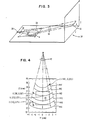
- the beam from a storage ring source is divergent in the horizontal plane (y direction) but highly collimated in a vertical plane (z direction). It is therefore similar to a horizontal fan of radiation which then must be moved vertically in order to expose a mask in the z direction.
- the horizontal divergence of the beam means that the illumination along the y direction may vary in different parts of the beam if a horizontally condensing optical system is used, if this beam is traversed in the z direction.
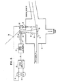
- a method for providing substantially uniform illumination of a two dimensional area with an input beam of radiation which is divergent in one direction comprises sending said beam from a source to a reflecting means from which it is reflected to said area to be illuminated, and collimating said beam to provide a collimated reflected beam to said area, characterised by changing the angle between said input beam and said reflecting means such that the product of the flux in said reflected beam and the velocity of movement of said beam is approximately constant with time as said reflected beam moves across said area.
- Fig. 2 shows the spectrum of power emitted from the source and also the power delivered to the mask plane.
- the width U of power delivered to the mask plane is shown for two wavelengths ⁇ 1 and A 2 .
- the power distribution in the mask plane depends upon the wavelength. This is one reason why it is difficult to provide uniform y-z illumination of a mask area with a beam such as beam 24 in Fig. 2. It is a problem that the present invention solves.
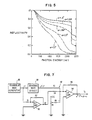
- the cylindrical scanning mirror 28 in Fig. 3 is chosen to have a high reflectivity for the wavelengths present in the input beam 32 (Fig. 3).
- the mirror is typically quartz coated with a heavy metal, such as gold. Gold is preferred because it is a heavy metal which provides a smooth surface and doesn't readily oxidize.
- an x-ray lithography system was modelled in which cylindrical mirrors had focal lengths ranging from 3.5 to 7 cms, where the source-mirror distance was 2 m and the mirror-mask distance was 8 m.
- the scan beam was swept vertically with an instantaneous intensity that was 3.2 to 5.0 times that for a plane mirror, the cylindrical mirror having a focal length of cms and a radius of 10 cms. At these angles of incidence, the transmission of radiation at x-ray lithography wavelengths from the mirror is approximately 70%.
Landscapes
- Physics & Mathematics (AREA)
- General Physics & Mathematics (AREA)
- Optics & Photonics (AREA)
- Exposure And Positioning Against Photoresist Photosensitive Materials (AREA)
- Exposure Of Semiconductors, Excluding Electron Or Ion Beam Exposure (AREA)
- Mechanical Optical Scanning Systems (AREA)
- Apparatus For Radiation Diagnosis (AREA)
Claims (13)
Applications Claiming Priority (2)
| Application Number | Priority Date | Filing Date | Title |
|---|---|---|---|
| US33648481A | 1981-12-31 | 1981-12-31 | |
| US336484 | 1981-12-31 |
Publications (3)
| Publication Number | Publication Date |
|---|---|
| EP0083394A2 EP0083394A2 (fr) | 1983-07-13 |
| EP0083394A3 EP0083394A3 (en) | 1983-08-10 |
| EP0083394B1 true EP0083394B1 (fr) | 1986-04-09 |
Family
ID=23316299
Family Applications (1)
| Application Number | Title | Priority Date | Filing Date |
|---|---|---|---|
| EP19820109182 Expired EP0083394B1 (fr) | 1981-12-31 | 1982-10-05 | Procédé et appareil pour l'illumination uniforme d'une surface |
Country Status (3)
| Country | Link |
|---|---|
| EP (1) | EP0083394B1 (fr) |
| JP (1) | JPS58118999A (fr) |
| DE (1) | DE3270459D1 (fr) |
Families Citing this family (22)
| Publication number | Priority date | Publication date | Assignee | Title |
|---|---|---|---|---|
| JPS5969927A (ja) * | 1982-10-15 | 1984-04-20 | Hitachi Ltd | X線露光装置 |
| JPS60156000A (ja) * | 1984-01-26 | 1985-08-16 | 工業技術院長 | 軟x線投射装置 |
| JPS60178627A (ja) * | 1984-02-24 | 1985-09-12 | Canon Inc | X線転写装置 |
| GB2155201B (en) * | 1984-02-24 | 1988-07-13 | Canon Kk | An x-ray exposure apparatus |
| JPH07407B2 (ja) * | 1985-01-07 | 1995-01-11 | キヤノン株式会社 | 印字制御方法 |
| DE3571353D1 (en) * | 1985-04-04 | 1989-08-10 | Hitachi Ltd | X-ray exposure system |
| JPS62178207A (ja) * | 1986-01-31 | 1987-08-05 | Dainippon Screen Mfg Co Ltd | 照明用の光学系 |
| JP2611762B2 (ja) * | 1986-12-01 | 1997-05-21 | キヤノン株式会社 | Sor露光装置 |
| JPS63301000A (ja) * | 1987-06-01 | 1988-12-08 | Canon Inc | 露光装置 |
| US5365561A (en) * | 1988-03-25 | 1994-11-15 | Canon Kabushiki Kaisha | Exposure control in an X-ray exposure apparatus |
| EP0357425B1 (fr) * | 1988-09-02 | 1996-11-06 | Canon Kabushiki Kaisha | Dispositif d'exposition |
| EP0359370B1 (fr) * | 1988-09-14 | 1996-01-03 | Canon Kabushiki Kaisha | Dispositif de contrÔle d'exposition dans un appareil d'exposition à rayons X |
| JP2770960B2 (ja) * | 1988-10-06 | 1998-07-02 | キヤノン株式会社 | Sor−x線露光装置 |
| US5285488A (en) * | 1989-09-21 | 1994-02-08 | Canon Kabushiki Kaisha | Exposure apparatus |
| DE69030348T2 (de) * | 1989-10-03 | 1997-09-04 | Canon K.K., Tokio/Tokyo | Belichtungsvorrichtung |
| US5182763A (en) * | 1989-12-28 | 1993-01-26 | Canon Kabushiki Kaisha | Reflection device |
| JP2742122B2 (ja) * | 1989-12-28 | 1998-04-22 | キヤノン株式会社 | 照明系及びx線露光装置 |
| DE69126719T2 (de) * | 1990-03-09 | 1997-11-06 | Canon K.K., Tokio/Tokyo | Belichtungsvorrichtung |
| JP2789514B2 (ja) * | 1994-06-20 | 1998-08-20 | キヤノン株式会社 | Sor露光装置 |
| JP2644692B2 (ja) * | 1995-01-30 | 1997-08-25 | キヤノン株式会社 | X線転写装置 |
| US6289076B1 (en) | 1997-05-06 | 2001-09-11 | Sumitomo Heavy Industries, Ltd. | Transmission system for synchrotron radiation light |
| CN112185833B (zh) * | 2019-07-01 | 2025-10-28 | 应用材料公司 | 在沉积腔室制造期间的微粒物的实时检测 |
Family Cites Families (7)
| Publication number | Priority date | Publication date | Assignee | Title |
|---|---|---|---|---|
| FR1000428A (fr) * | 1948-11-29 | 1952-02-12 | Rech S Et Ind | Catoptrique à radiations électromagnétiques à ondes courtes |
| US3925785A (en) * | 1974-08-09 | 1975-12-09 | Bell Telephone Labor Inc | Pattern generating apparatus |
| US4028547A (en) * | 1975-06-30 | 1977-06-07 | Bell Telephone Laboratories, Incorporated | X-ray photolithography |
| JPS5430854A (en) * | 1977-08-12 | 1979-03-07 | Canon Inc | Two-dimensional scanner |
| FR2455298A1 (fr) * | 1979-04-23 | 1980-11-21 | Thomson Csf | Dispositif illuminateur destine a fournir un faisceau d'eclairement divergent a partir d'une zone predeterminee d'un plan et systeme de transfert de motifs comprenant un tel dispositif |
| JPS5642343A (en) * | 1979-09-14 | 1981-04-20 | Jeol Ltd | Exposing method of electron beam |
| JPS5645024A (en) * | 1979-09-21 | 1981-04-24 | Chiyou Lsi Gijutsu Kenkyu Kumiai | Lithography apparatus |
-
1982
- 1982-10-05 EP EP19820109182 patent/EP0083394B1/fr not_active Expired
- 1982-10-05 DE DE8282109182T patent/DE3270459D1/de not_active Expired
- 1982-10-27 JP JP57187670A patent/JPS58118999A/ja active Pending
Also Published As
| Publication number | Publication date |
|---|---|
| EP0083394A3 (en) | 1983-08-10 |
| DE3270459D1 (en) | 1986-05-15 |
| JPS58118999A (ja) | 1983-07-15 |
| EP0083394A2 (fr) | 1983-07-13 |
Similar Documents
| Publication | Publication Date | Title |
|---|---|---|
| EP0083394A2 (fr) | Procédé et appareil pour l'illumination uniforme d'une surface | |
| US6713747B2 (en) | Light exposure apparatus | |
| US4028547A (en) | X-ray photolithography | |
| EP0424134B1 (fr) | Appareil pour l'exposition aux rayons X | |
| EP0416811B1 (fr) | Procédé et appareil pour l'exposition aux rayons x | |
| US7298453B2 (en) | Method and apparatus for irradiating a microlithographic substrate | |
| GB2244820A (en) | X-ray lithography beamline method and apparatus. | |
| US5268951A (en) | X-ray beam scanning method for producing low distortion or constant distortion in x-ray proximity printing | |
| EP0109193B1 (fr) | Système lithographique aux rayons X | |
| EP0389259B1 (fr) | Appareil pour l'exposition aux rayons X | |
| Windt et al. | Soft x-ray reflectometry of multilayer coatings using a laser-plasma source | |
| US6280906B1 (en) | Method of imaging a mask pattern on a substrate by means of EUV radiation, and apparatus and mask for performing the method | |
| Tarrio et al. | Towards high accuracy reflectometry for extreme-ultraviolet lithography | |
| Basov et al. | Two-dimensional X-ray focusing by a phase Fresnel zone plate at grazing incidence | |
| US5182763A (en) | Reflection device | |
| Tichenor et al. | Development of a laboratory extreme-ultraviolet lithography tool | |
| EP0435644B1 (fr) | Dispositif de balayage | |
| JPH0246717A (ja) | X線露光方法 | |
| JPH04120717A (ja) | X線露光装置 | |
| JPH0527080B2 (fr) | ||
| JP2001066399A (ja) | 多層膜反射鏡および露光装置、又は分析装置。 | |
| JP2980397B2 (ja) | X線露光装置 | |
| JPH1126350A (ja) | 露光装置 | |
| Gutman et al. | Multilayer Performance for Soft X-ray Schwarzchild Optics | |
| Erko et al. | Bragg-Fresnel optics and supermirrors |
Legal Events
| Date | Code | Title | Description |
|---|---|---|---|
| PUAI | Public reference made under article 153(3) epc to a published international application that has entered the european phase |
Free format text: ORIGINAL CODE: 0009012 |
|
| PUAL | Search report despatched |
Free format text: ORIGINAL CODE: 0009013 |
|
| AK | Designated contracting states |
Designated state(s): DE FR GB |
|
| AK | Designated contracting states |
Designated state(s): DE FR GB |
|
| 17P | Request for examination filed |
Effective date: 19831021 |
|
| GRAA | (expected) grant |
Free format text: ORIGINAL CODE: 0009210 |
|
| AK | Designated contracting states |
Kind code of ref document: B1 Designated state(s): DE FR GB |
|
| REF | Corresponds to: |
Ref document number: 3270459 Country of ref document: DE Date of ref document: 19860515 |
|
| ET | Fr: translation filed | ||
| PLBE | No opposition filed within time limit |
Free format text: ORIGINAL CODE: 0009261 |
|
| STAA | Information on the status of an ep patent application or granted ep patent |
Free format text: STATUS: NO OPPOSITION FILED WITHIN TIME LIMIT |
|
| 26N | No opposition filed | ||
| PGFP | Annual fee paid to national office [announced via postgrant information from national office to epo] |
Ref country code: GB Payment date: 19920925 Year of fee payment: 11 |
|
| PGFP | Annual fee paid to national office [announced via postgrant information from national office to epo] |
Ref country code: FR Payment date: 19920928 Year of fee payment: 11 |
|
| PGFP | Annual fee paid to national office [announced via postgrant information from national office to epo] |
Ref country code: DE Payment date: 19921027 Year of fee payment: 11 |
|
| PG25 | Lapsed in a contracting state [announced via postgrant information from national office to epo] |
Ref country code: GB Effective date: 19931005 |
|
| GBPC | Gb: european patent ceased through non-payment of renewal fee |
Effective date: 19931005 |
|
| PG25 | Lapsed in a contracting state [announced via postgrant information from national office to epo] |
Ref country code: FR Effective date: 19940630 |
|
| PG25 | Lapsed in a contracting state [announced via postgrant information from national office to epo] |
Ref country code: DE Effective date: 19940701 |
|
| REG | Reference to a national code |
Ref country code: FR Ref legal event code: ST |