EP0083411A2 - Photodétecteur digital - Google Patents
Photodétecteur digital Download PDFInfo
- Publication number
- EP0083411A2 EP0083411A2 EP82110813A EP82110813A EP0083411A2 EP 0083411 A2 EP0083411 A2 EP 0083411A2 EP 82110813 A EP82110813 A EP 82110813A EP 82110813 A EP82110813 A EP 82110813A EP 0083411 A2 EP0083411 A2 EP 0083411A2
- Authority
- EP
- European Patent Office
- Prior art keywords
- region
- conductivity type
- photodetector
- intrinsic
- digital
- Prior art date
- Legal status (The legal status is an assumption and is not a legal conclusion. Google has not performed a legal analysis and makes no representation as to the accuracy of the status listed.)
- Granted
Links
Images

Classifications
-
- H—ELECTRICITY
- H10—SEMICONDUCTOR DEVICES; ELECTRIC SOLID-STATE DEVICES NOT OTHERWISE PROVIDED FOR
- H10F—INORGANIC SEMICONDUCTOR DEVICES SENSITIVE TO INFRARED RADIATION, LIGHT, ELECTROMAGNETIC RADIATION OF SHORTER WAVELENGTH OR CORPUSCULAR RADIATION
- H10F39/00—Integrated devices, or assemblies of multiple devices, comprising at least one element covered by group H10F30/00, e.g. radiation detectors comprising photodiode arrays
- H10F39/10—Integrated devices
- H10F39/103—Integrated devices the at least one element covered by H10F30/00 having potential barriers, e.g. integrated devices comprising photodiodes or phototransistors
-
- H—ELECTRICITY
- H03—ELECTRONIC CIRCUITRY
- H03K—PULSE TECHNIQUE
- H03K17/00—Electronic switching or gating, i.e. not by contact-making and –breaking
- H03K17/51—Electronic switching or gating, i.e. not by contact-making and –breaking characterised by the components used
- H03K17/78—Electronic switching or gating, i.e. not by contact-making and –breaking characterised by the components used using opto-electronic devices, i.e. light-emitting and photoelectric devices electrically- or optically-coupled
- H03K17/785—Electronic switching or gating, i.e. not by contact-making and –breaking characterised by the components used using opto-electronic devices, i.e. light-emitting and photoelectric devices electrically- or optically-coupled controlling field-effect transistor switches
Definitions
- the technical field of the invention is the conversion of optical signals to digital form.
- circuits of this type it is necessary to sense the optical signal and then circuitry is required to provide sufficient digital integrity along with matching capability to drive the responding circuits.
- a photodetector circuit generally must provide the necessary power gain since very little power is transferred in the optical signal.
- the digital signal is precise but the response rate has limits.
- the bistability in the output driver is of advantage for precision in digital signals.
- a digital photodetector technique incorporates photoresponsiveness into a source follower-inverter type of circuit to provide a defined binary output electric signal in response to a selectable optical signal strength and threshold.
- a photoresponsive section of the circuit is a source-follower type of circuit stage having as one branch a photodetecting element 1 which may be any photosensitive device such as a photoconductor, a PIN diode or a phototransistor having a high dark resistance.
- the photodetector 1 is shown receiving input light 2 and has one electrode thereof connected to ground.
- the second electrode of element 1 is connected through a depletion mode field effect transistor (FET) 3 having the gate thereof connected to the source electrode thereof in the standard source-follower type circuit method and having the drain electrode thereof connected to a drive voltage (B + ).
- FET depletion mode field effect transistor
- depletion mode FET transistors which have different conduction threshold from enhancement mode transistors, are labelled D and E, respectively.
- An enhancement mode FET (E) may be rendered completely non-conductive when the gate to source voltage is equal or less than zero or "normally off".
- the circuit point or node at the output of the light sensitive element 1 and the source electrode of the load field effect transistor 3 is labelled 4.
- the signal from node 4 is labelled V 1 and is connected to the gate electrode 5 of an enhancement mode FET transistor 6.
- the source electrode 7 of transistor 6 is connected to ground and the drain electrode thereof is connected to an output circuit node 8.
- the node 8 in turn is connected to the source electrode of a depletion mode type FET transistor 9, the gate 10 of which is also connected to the node 8.
- the drain electrode 11 of transistor 9 is connected to the drive voltage (B + ).
- the output signal labelled V 2 is taken from the node 8.
- the device 1 In operation, in the absence of an optical signal 2, the device 1 is nonconducting or "off” and the device 3 is conducting or "on". This causes the V 1 signal at the node 4 to assume the level of the B voltage.
- this condition appears at gate 5 which places the transistor 6 in the output inverter stage fully conductive or "on” while the depletion mode FET device 9 controls the current so that the output V at node 8 is near zero or ground potential.
- the switching of the photoresponsive stage and the enhancement depletion inverter are extremely fast and non-linear when high performance FET devices are used.
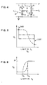
- the operational input/output transfer characteristics of the circuit of FIG. 1 may be seen by referring to the graphs of FIGS. 2 and 3.
- FIG. 2 there is shown an operating characteristic graph of the circuit of FIG. 1. There are two quasi monostable states associated respectively with dark and light conditions.
- FIG. 2 shows the transfer characteristics of the signal V 1 versus input light as a dashed curve and of the signal V 2 versus V 1 as a solid curve.
- FIG. 3 there is shown an operating characteristic graph of light input I L versus resulting voltage output V 2 which illustrates the switching thresholds I THl and I TH2 .
- the threshold of the two quasi monostable states of the circuit is the region between the dashed lines. These states can be fine-tuned by selecting the threshold voltages of the field effect transistors in the usual manner well known in the art.
- the advantages may be further enhanced by the use of light responsive members in a push-pull relationship as set forth in connection with FIG. 4.
- the circuit is similar to that of FIG. 1 except that the depletion mode FET 9 in the output stage is replaced by a second light sensitive element 1B.
- the light sensitive elements are labelled elements lA and 1B and the sources of light are labelled 2A and 2B.
- the two photosensitive members operate in complementary fashion.
- the stage involving light element 1A operates identically to that shown in FIG. 1.
- the optically produced current flow through the optical signal responsive member 1B increases conduction and changes the output level at node 8.
- both devices lA and 1B are non-conductive. Under these conditions, the enhancement FET device 6 is "on" because the node 4 is at B + .
- the V 2 output at node 8 is essentially at zero or ground.
- the sensing devices 1A and 1B are both turned on and produce photo current. This results in a push-pull effect on the circuit and the signal at the output V rapidly approaches + B + .
- the switching operations are monostable and exhibit a fast digital pulse detection at a defined threshold.
- V 1 versus I L is the dashed curve whereas V 2 versus V 1 performed segments are the solid lines with the dot-dash connectors.
- FIG. 6 there is plotted light input I L and voltage output V characteristics illustrating the two thresholds I THl and I TH2 .
- the two monostable states associated with light signal conditions are illustrated and the switching is complete from both directions, dark to light and vice versa at the respective threshold I TH1 and I TH2 .
- the window of switching between thresholds can be fine tuned by the threshold of the FETs. For instance, I THl and I TH2 can be made closer to each other by adjusting threshold voltages for both the enhancement and depletion FET devices.
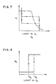
- FIGS. 7 and 8 the circuit operation graphs or transfer characteristics of quasi bistable switching and the light input versus voltage output characteristics are shown.
- FIG. 7 a graph is shown of the quasi bistable switching of the circuit of FIG. 4 wherein V 1 versus I L is shown as the dashed curve and V 2 versus V 1 is shown as the solid line with the dashed connectors.
- FIG. 8 there is plotted light input versus voltage output for quasi bistable switching and here it is shown that the threshold current values for the respective conditions I THl and I TH2 overlap illustrating hysteretic switching behaviour. This capability when properly tuned for narrow switching windows permits the device to serve as a binary digitizer.
- the circuit of the invention has several capabilities that result in advantages.
- the nonlinearity of the inverter circuit type transfer characteristics which provide threshold switching and binary signal definition to the circuit also provides power gain right at the sensing stage. -These capabilities provide the advantage of a high signal-to-noise ratio.
- a high electric field is always present at the optical sensing elements when they are dark so that small optically generated carrier transit times are encountered during the critical turn-on and turn-off parts of the switching. This provides the advantage of fast detection of optical pulse signals and provides precision of the digital output.
- the optical signal detectors can be either photo- conductors, photodiodes or phototransistors.
- the output signal level is determined by the B voltage level.
- the principles of the invention are preferably embodied in an integrated solid state structure wherein the FET transistors and optical signal detectors are extrinsic regions in an intrinsic portion of a monolithic semiconductor body.
- FIG. 9 an integrated structure is provided containing the capabilities of the circuit of FIG. 1 and employing the same reference numerals.
- the optical signal detector 1 is the N + I P + diode.
- Three FET transistors are provided, the two depletion FET's 3 and 9 are labelled D and the enhancement FET is labelled E.
- the two depletion devices D which are normally on, are formed by phosphorus implantations of the channels standard in the art.
- the enhancement FET E which is normally off, is formed by boron 'implantation of the channel standard in the art.
- the structure of FIG. 9 is fabricated by starting, for example, with a p +- type silicon wafer on which an intrinsic (I) region is epitaxially grown.
- the N + source/drain regions are diffused as well as the contact ring region for the PIN diode.
- Three regions will next be implanted to suitable dopant, dosage and energy to form shallow N + for the PIN diode, lightly N region for the depletion FETs 3 and 9, and lightly P region for the enhancement FET device 6. It is possible to have the N + contact region and shallow N + region for the PIN diode structure done in the same process step provided the N + region for the source and drain contacts are sufficiently shallow.
- the push-pull arrangement of FIG. 4 may be fabricated in a monolithic structure as shown in FIG. 10 wherein the same reference numerals are employed.
- a deep trench 10 is provided for isolation.
- the structure is formed starting, for example, with an N silicon substrate.
- An epitaxial P layer is grown followed thereafter by an intrinsic layer I.
- a deep trench in the form of a closed horizontal configuration surrounding each device segment is provided with the crosssectional elements thereof shown as elements 10.
- the trench is back filled with Si0 2 or other suitable insulating material to form the isolation.
- a suitable contact 11 to the P region can be accomplished by a standard "reach through" diffusion at a designated area using boron.
- the N + source/drain region and the shallow N + PIN contact region can be processed in the same step if the source/drain regions are shallow enough for the purpose of photodiode.
Landscapes
- Solid State Image Pick-Up Elements (AREA)
- Electronic Switches (AREA)
- Light Receiving Elements (AREA)
Applications Claiming Priority (2)
| Application Number | Priority Date | Filing Date | Title |
|---|---|---|---|
| US336490 | 1981-12-31 | ||
| US06/336,490 US4447746A (en) | 1981-12-31 | 1981-12-31 | Digital photodetectors |
Publications (3)
| Publication Number | Publication Date |
|---|---|
| EP0083411A2 true EP0083411A2 (fr) | 1983-07-13 |
| EP0083411A3 EP0083411A3 (en) | 1985-08-07 |
| EP0083411B1 EP0083411B1 (fr) | 1988-07-27 |
Family
ID=23316333
Family Applications (1)
| Application Number | Title | Priority Date | Filing Date |
|---|---|---|---|
| EP82110813A Expired EP0083411B1 (fr) | 1981-12-31 | 1982-11-23 | Photodétecteur digital |
Country Status (4)
| Country | Link |
|---|---|
| US (1) | US4447746A (fr) |
| EP (1) | EP0083411B1 (fr) |
| JP (1) | JPS58119232A (fr) |
| DE (1) | DE3278845D1 (fr) |
Cited By (9)
| Publication number | Priority date | Publication date | Assignee | Title |
|---|---|---|---|---|
| FR2589006A1 (fr) * | 1985-10-21 | 1987-04-24 | Telemecanique Electrique | Circuit de commande par voie optique d'une structure commandee a electrode de declenchement isolee, et circuit comportant une telle structure |
| GB2194389A (en) * | 1986-08-20 | 1988-03-02 | Agency Ind Science Techn | Optical control circuit and semiconductor device |
| EP0284895A1 (fr) * | 1987-03-17 | 1988-10-05 | Bayerische Motoren Werke Aktiengesellschaft, Patentabteilung AJ-3 | Méthode pour le gonflement d'un pneumatique de véhicule sous une pression correcte avec un dispositif pour le contrôle de la pression de pneumatiques |
| EP0307911A3 (en) * | 1987-09-17 | 1989-06-07 | Amskan Limited | Signal discriminator |
| GB2258759A (en) * | 1991-08-14 | 1993-02-17 | Tandberg Data | Integrated opto-electronic sensor for pulsed light |
| WO1994028582A1 (fr) * | 1993-06-01 | 1994-12-08 | The University Of North Carolina | Circuit integre a transistors complementaires a effet de champ et a photodetecteurs, et son procede de fabrication |
| EP0658003A1 (fr) * | 1993-12-09 | 1995-06-14 | AT&T Corp. | Appareil et méthode pour établir les références d'un récepteur optique |
| EP0691742A3 (fr) * | 1994-07-05 | 1997-09-03 | At & T Corp | Récepteur optique avec un préamplificateur à impédance élevée |
| WO2013083889A1 (fr) * | 2011-12-08 | 2013-06-13 | Societe Francaise De Detecteurs Infrarouges - Sofradir | Dispositif de détection de rayonnement électromagnétique impulsionnel |
Families Citing this family (13)
| Publication number | Priority date | Publication date | Assignee | Title |
|---|---|---|---|---|
| US4691111A (en) * | 1984-04-05 | 1987-09-01 | The United States Of America As Represented By The Secretary Of The Army | Multiple gap optically activated switch |
| US4771325A (en) * | 1985-02-11 | 1988-09-13 | American Telephone & Telegraph Co., At&T Bell Laboratories | Integrated photodetector-amplifier device |
| US4754312A (en) * | 1987-04-07 | 1988-06-28 | The United States Of America As Represented By The Secretary Of The Air Force | Integratable differential light detector |
| FR2640044B1 (fr) * | 1988-12-06 | 1993-02-12 | Thomson Csf | Dispositif de detection de rayonnements optiques |
| JPH02308575A (ja) * | 1989-05-24 | 1990-12-21 | Nissan Motor Co Ltd | 光検出セル |
| EP0400399A3 (fr) * | 1989-05-31 | 1991-05-29 | Siemens Aktiengesellschaft | Intégration monolithique d'une combinaison photodiode FET |
| US5241575A (en) * | 1989-12-21 | 1993-08-31 | Minolta Camera Kabushiki Kaisha | Solid-state image sensing device providing a logarithmically proportional output signal |
| US5289286A (en) * | 1991-07-18 | 1994-02-22 | Minolta Camera Kabushiki Kaisha | Solid state sensor having logarithmic photovoltaic response, with pixel uniformity correction and white balance circuitry therefor |
| JPH05219443A (ja) * | 1992-02-05 | 1993-08-27 | Minolta Camera Co Ltd | 固体撮像装置 |
| US7264982B2 (en) * | 2004-11-01 | 2007-09-04 | International Business Machines Corporation | Trench photodetector |
| US20060239173A1 (en) * | 2005-04-25 | 2006-10-26 | Yi Zhang | Optical storage with direct digital optical detection |
| US8058675B2 (en) * | 2006-12-27 | 2011-11-15 | Semiconductor Energy Laboratory Co., Ltd. | Semiconductor device and electronic device using the same |
| KR101536194B1 (ko) * | 2008-05-19 | 2015-07-13 | 삼성디스플레이 주식회사 | 액정 표시 장치와 그 구동 방법 |
Family Cites Families (25)
| Publication number | Priority date | Publication date | Assignee | Title |
|---|---|---|---|---|
| US27867A (en) * | 1860-04-10 | Improvement in sewing-machines | ||
| US3582220A (en) * | 1968-02-21 | 1971-06-01 | Asahi Optical Co Ltd | Light contrast meter for measuring the difference between maximum light intensity and immediately incident light intensity or other intensity |
| US3590153A (en) * | 1968-09-13 | 1971-06-29 | Nippon Electric Co | Solid-state image scanner |
| US3619665A (en) * | 1969-10-15 | 1971-11-09 | Rca Corp | Optically settable flip-flop |
| US3631411A (en) * | 1969-10-15 | 1971-12-28 | Rca Corp | Electrically and optically accessible memory |
| US3624419A (en) * | 1970-10-19 | 1971-11-30 | Rca Corp | Balanced optically settable memory cell |
| US3742830A (en) * | 1971-07-06 | 1973-07-03 | Olympus Optical Co | Information holding apparatus |
| US3770968A (en) * | 1972-02-24 | 1973-11-06 | Ibm | Field effect transistor detector amplifier cell and circuit for low level light signals |
| US3770967A (en) * | 1972-02-24 | 1973-11-06 | Ibm | Field effect transistor detector amplifier cell and circuit providing a digital output and/or independent of background |
| USRE27867E (en) | 1972-05-05 | 1974-01-01 | Radiation-sensitive camera shutter and aperture control systems | |
| US3891936A (en) * | 1972-06-26 | 1975-06-24 | Trw Inc | Low frequency field effect amplifier |
| US3748498A (en) * | 1972-07-27 | 1973-07-24 | American Micro Syst | Low voltage quasi static flip-flop |
| US3870901A (en) * | 1973-12-10 | 1975-03-11 | Gen Instrument Corp | Method and apparatus for maintaining the charge on a storage node of a mos circuit |
| JPS5430617B2 (fr) * | 1974-09-04 | 1979-10-02 | ||
| JPS5179540A (en) * | 1975-01-06 | 1976-07-10 | Hitachi Ltd | Dengentonyugono shokijotaisetsuteikairo |
| US4023122A (en) * | 1975-01-28 | 1977-05-10 | Nippon Electric Company, Ltd. | Signal generating circuit |
| JPS5619786B2 (fr) * | 1975-02-20 | 1981-05-09 | ||
| US4004170A (en) * | 1975-04-29 | 1977-01-18 | International Business Machines Corporation | MOSFET latching driver |
| US4011471A (en) * | 1975-11-18 | 1977-03-08 | The United States Of America As Represented By The Secretary Of The Air Force | Surface potential stabilizing circuit for charge-coupled devices radiation hardening |
| JPS5631717Y2 (fr) * | 1975-12-09 | 1981-07-29 | ||
| US4023048A (en) * | 1975-12-15 | 1977-05-10 | International Business Machines Corporation | Self-scanning photo-sensitive circuits |
| FR2356328A1 (fr) * | 1976-06-24 | 1978-01-20 | Ibm France | Dispositif d'elimination du bruit dans les reseaux photosensibles a auto-balayage |
| US4065668A (en) * | 1976-07-22 | 1977-12-27 | National Semiconductor Corporation | Photodiode operational amplifier |
| US4183034A (en) * | 1978-04-17 | 1980-01-08 | International Business Machines Corp. | Pin photodiode and integrated circuit including same |
| US4202044A (en) * | 1978-06-13 | 1980-05-06 | International Business Machines Corporation | Quaternary FET read only memory |
-
1981
- 1981-12-31 US US06/336,490 patent/US4447746A/en not_active Expired - Lifetime
-
1982
- 1982-10-19 JP JP57182219A patent/JPS58119232A/ja active Granted
- 1982-11-23 DE DE8282110813T patent/DE3278845D1/de not_active Expired
- 1982-11-23 EP EP82110813A patent/EP0083411B1/fr not_active Expired
Cited By (14)
| Publication number | Priority date | Publication date | Assignee | Title |
|---|---|---|---|---|
| FR2589006A1 (fr) * | 1985-10-21 | 1987-04-24 | Telemecanique Electrique | Circuit de commande par voie optique d'une structure commandee a electrode de declenchement isolee, et circuit comportant une telle structure |
| GB2194389A (en) * | 1986-08-20 | 1988-03-02 | Agency Ind Science Techn | Optical control circuit and semiconductor device |
| GB2194389B (en) * | 1986-08-20 | 1990-02-14 | Agency Ind Science Techn | Optical control circuit and semiconductor device for realizing the circuit |
| EP0284895A1 (fr) * | 1987-03-17 | 1988-10-05 | Bayerische Motoren Werke Aktiengesellschaft, Patentabteilung AJ-3 | Méthode pour le gonflement d'un pneumatique de véhicule sous une pression correcte avec un dispositif pour le contrôle de la pression de pneumatiques |
| EP0307911A3 (en) * | 1987-09-17 | 1989-06-07 | Amskan Limited | Signal discriminator |
| DE4226585A1 (de) * | 1991-08-14 | 1993-02-18 | Tandberg Data | Monolithischer integrierter schaltkreis fuer gepulstes licht |
| GB2258759A (en) * | 1991-08-14 | 1993-02-17 | Tandberg Data | Integrated opto-electronic sensor for pulsed light |
| GB2258759B (en) * | 1991-08-14 | 1995-06-28 | Tandberg Data | High dynamic range integrated opto-electronic sensor for pulsed light |
| WO1994028582A1 (fr) * | 1993-06-01 | 1994-12-08 | The University Of North Carolina | Circuit integre a transistors complementaires a effet de champ et a photodetecteurs, et son procede de fabrication |
| EP0658003A1 (fr) * | 1993-12-09 | 1995-06-14 | AT&T Corp. | Appareil et méthode pour établir les références d'un récepteur optique |
| EP0691742A3 (fr) * | 1994-07-05 | 1997-09-03 | At & T Corp | Récepteur optique avec un préamplificateur à impédance élevée |
| WO2013083889A1 (fr) * | 2011-12-08 | 2013-06-13 | Societe Francaise De Detecteurs Infrarouges - Sofradir | Dispositif de détection de rayonnement électromagnétique impulsionnel |
| FR2983972A1 (fr) * | 2011-12-08 | 2013-06-14 | Soc Fr Detecteurs Infrarouges Sofradir | Dispositif de detection de rayonnement electromagnetique impulsionnel |
| US9520844B2 (en) | 2011-12-08 | 2016-12-13 | SOCIÉTÉ FRANçAISE DE DÉTECTEURS INFRAROUGES-SOFRADIR | Electromagnetic radiation detection circuit for pulse detection including an amplifying transistor and a coupling capacitor |
Also Published As
| Publication number | Publication date |
|---|---|
| EP0083411A3 (en) | 1985-08-07 |
| JPH034137B2 (fr) | 1991-01-22 |
| JPS58119232A (ja) | 1983-07-15 |
| US4447746A (en) | 1984-05-08 |
| EP0083411B1 (fr) | 1988-07-27 |
| DE3278845D1 (en) | 1988-09-01 |
Similar Documents
| Publication | Publication Date | Title |
|---|---|---|
| EP0083411B1 (fr) | Photodétecteur digital | |
| US4390790A (en) | Solid state optically coupled electrical power switch | |
| US5592124A (en) | Integrated photodiode/transimpedance amplifier | |
| EP0158186B1 (fr) | Dispositif à thyristor extinguible par la lumière | |
| CA1285033C (fr) | Relais a semiconducteur a circuit de decharge a thyristor | |
| US4814836A (en) | FET photoconductor with a heterojunction in the channel | |
| JPS59107578A (ja) | 半導体光電変換装置 | |
| US4717947A (en) | Semiconductor device turned on and off by light | |
| US4494132A (en) | Semiconductor opto-electronic switch | |
| JPS6259902B2 (fr) | ||
| US4143266A (en) | Method and device for detecting radiatons | |
| US3868718A (en) | Field effect transistor having a pair of gate regions | |
| EP0480412B1 (fr) | Dispositif à transfer et/ou amplification de charges | |
| US4250409A (en) | Control circuitry using a pull-down transistor for high voltage field terminated diode solid-state switches | |
| EP0242523A2 (fr) | Etage d'attaque intégré pour circuit logique à Fet | |
| JPH02239498A (ja) | トランジスタを備えるマイクロ波サンプルホールド装置 | |
| EP0052633B1 (fr) | Dispositif a commutation optique | |
| US3454795A (en) | Semiconductive field-controlled diode device | |
| JPS633456A (ja) | 固体撮像装置 | |
| JPH05167412A (ja) | 半導体リレー回路 | |
| KR960014724B1 (ko) | 전하검출소자 | |
| Hata et al. | Silicon pin photodetectors with integrated transistor amplifiers | |
| JP2560203B2 (ja) | 集積化受光素子 | |
| Ando et al. | Planar InP avalanche photodiode with Zn-diffused guard ring | |
| JPH0444469B2 (fr) |
Legal Events
| Date | Code | Title | Description |
|---|---|---|---|
| PUAI | Public reference made under article 153(3) epc to a published international application that has entered the european phase |
Free format text: ORIGINAL CODE: 0009012 |
|
| AK | Designated contracting states |
Designated state(s): DE FR GB |
|
| 17P | Request for examination filed |
Effective date: 19831021 |
|
| PUAL | Search report despatched |
Free format text: ORIGINAL CODE: 0009013 |
|
| AK | Designated contracting states |
Designated state(s): DE FR GB |
|
| 17Q | First examination report despatched |
Effective date: 19870924 |
|
| GRAA | (expected) grant |
Free format text: ORIGINAL CODE: 0009210 |
|
| AK | Designated contracting states |
Kind code of ref document: B1 Designated state(s): DE FR GB |
|
| REF | Corresponds to: |
Ref document number: 3278845 Country of ref document: DE Date of ref document: 19880901 |
|
| ET | Fr: translation filed | ||
| PLBE | No opposition filed within time limit |
Free format text: ORIGINAL CODE: 0009261 |
|
| STAA | Information on the status of an ep patent application or granted ep patent |
Free format text: STATUS: NO OPPOSITION FILED WITHIN TIME LIMIT |
|
| 26N | No opposition filed | ||
| PGFP | Annual fee paid to national office [announced via postgrant information from national office to epo] |
Ref country code: GB Payment date: 19921027 Year of fee payment: 11 |
|
| PGFP | Annual fee paid to national office [announced via postgrant information from national office to epo] |
Ref country code: DE Payment date: 19921121 Year of fee payment: 11 |
|
| PGFP | Annual fee paid to national office [announced via postgrant information from national office to epo] |
Ref country code: FR Payment date: 19931103 Year of fee payment: 12 |
|
| PG25 | Lapsed in a contracting state [announced via postgrant information from national office to epo] |
Ref country code: GB Effective date: 19931123 |
|
| GBPC | Gb: european patent ceased through non-payment of renewal fee |
Effective date: 19931123 |
|
| PG25 | Lapsed in a contracting state [announced via postgrant information from national office to epo] |
Ref country code: DE Effective date: 19940802 |
|
| PG25 | Lapsed in a contracting state [announced via postgrant information from national office to epo] |
Ref country code: FR Effective date: 19950731 |
|
| REG | Reference to a national code |
Ref country code: FR Ref legal event code: ST |