EP0084260A1 - Integerierte Halbleiterschaltung mit Prüfschaltung - Google Patents
Integerierte Halbleiterschaltung mit Prüfschaltung Download PDFInfo
- Publication number
- EP0084260A1 EP0084260A1 EP82306939A EP82306939A EP0084260A1 EP 0084260 A1 EP0084260 A1 EP 0084260A1 EP 82306939 A EP82306939 A EP 82306939A EP 82306939 A EP82306939 A EP 82306939A EP 0084260 A1 EP0084260 A1 EP 0084260A1
- Authority
- EP
- European Patent Office
- Prior art keywords
- level
- pin
- internal node
- mis
- power source
- Prior art date
- Legal status (The legal status is an assumption and is not a legal conclusion. Google has not performed a legal analysis and makes no representation as to the accuracy of the status listed.)
- Granted
Links
Images


Classifications
-
- G—PHYSICS
- G01—MEASURING; TESTING
- G01R—MEASURING ELECTRIC VARIABLES; MEASURING MAGNETIC VARIABLES
- G01R31/00—Arrangements for testing electric properties; Arrangements for locating electric faults; Arrangements for electrical testing characterised by what is being tested not provided for elsewhere
- G01R31/26—Testing of individual semiconductor devices
-
- G—PHYSICS
- G06—COMPUTING OR CALCULATING; COUNTING
- G06F—ELECTRIC DIGITAL DATA PROCESSING
- G06F11/00—Error detection; Error correction; Monitoring
- G06F11/006—Identification
Definitions
- the present invention relates to a semiconductor integrated circuit (IC) device, more particularly to a test circuit for an IC device which contains a variety of semiconductor integrated circuits in a chip thereof.
- IC semiconductor integrated circuit
- IC's are usually mass produced from the viewpoint of reduction of unit costs and standardization of capabilities. Such economic considerations, etc. make it advantageous to mass produce IC's having a main-semiconductor circuit and a sub-semiconductor circuit as an option at one time.
- the mass produced optional semiconductor circuits of each IC chip are then selectively made active by prepackaging wire bonding in accordance with individual user needs.
- a dynamic metal insulated semiconductor (MIS) memory circuit is generally used together with a so-called refresh counter.
- the aforesaid main-semiconductor circuit may be used for the dynamic MIS memory circuit, and the aforesaid sub-semiconductor circuit may be used for the refresh counter.
- the IC products are usually tested to confirm whether they contain both active main- and sub--semiconductor circuits or only active main-semiconductor circuits.
- the IC packages are then labeled according to the results of the tests.
- a predetermined test signal is externally supplied to the IC package under testing to cause IC to perform an operation based on the signal. If the results of the test confirm the operation of a first function, it is concluded that the IC product has only an active main-semiconductor circuit. contrary to the this, if they confirm the operation of a second function, it is concluded that the IC product has both active main- and sub-semiconductor circuits.
- the IC product includes only a main-semiconductor circuit or both a main-semiconductor circuit and active sub-semiconductor circuit depend on whether the sub-semiconductor circuit is commonly connected to a pin leading to an external power source. In activating the sub-semiconductor circuit, it is also necessary to connect its input ports to the specified pins of the IC package.
- the pads V cc and V cc * are particularly relevant to the embodiment of the present invention.
- the pad V cc constitutes a first power source with the ground levle pad V .
- the pad V * constitutes a second power source with ground level pad V.
- the first and second power sources drive the first and second semiconductor IC's I and II, respectively.
- the pads V cc and V cc * are commonly connected,through wire bondings 12 and 13, respectively, to a single pin 11 connected to an external power source (not shown). Such common pin occupation is preferable in view of economical use of the fixed number of pins.
- the wire bonding 12 is always provided.
- the wire bonding 13 is provided in accordance with individual user needs, as previously mentioned.
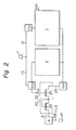
- FIG. 2 is a circuit diagram of a semiconductor circuit having a test circuit according to an embodiment of the present invention.
- a block 20 indicated by chain-dotted lines represents a test circuit, a particularly important part of the present invention.
- the test circuit 20 is connected to the pad A, the pad V cc *, and the pad V ss via newly employed lines 21, 22, and 23, respectively.
- the pad A is just an example; any otner pad may be used instead.
- the pad A is connected to an external I/O pin.
- the test circuit 20 is comprised of a series-connected MIS transistor 24 and an MIS diode 25.
- the gate of the MIS transistor 24 is connected to the line 22.
- the test circuit 20 functions to detect the existence of the wire bonding 13. From the viewpoint of the general purpose application of the present invention, however, the test circuit 20 functions to detect the level at an internal node N under testing, in which either one of the ground level (V ss ) ) or the power source level (V ) occurs at the pad V cc * (or at the internal node N to be tested).
- Figure 3A is an equivalent circuit diagram of the test circuit created under a mode where the second semiconductor IC II is active.
- Figure 3B is an equivalent circuit diagram of the test circuit created under a mode where the second semiconductor IC II is not active.
- the existence of the wire bonding 13 shown in Fig. 1 is detected by way of an external I/O pin.
- the power source level or the ground level occurring at the particular internal node N is detected by way of the external I/O pin.
- the pad V cc * is not activated.
- the pad V cc * is also connected, via a resistor having high resistance (not shown) to the ground, the pad V cc * is set at the ground level. Therefore, the level of the second power source for the second semiconductor IC II is set at the ground level. Accordingly, the ground level is applied to the gate of the MIS transistor 24. Similarly, when the node N is set at the ground level, that ground level is applied to the gate of the MIS transistor 24.
- Such a mode corresponds to the equivalent circuit diagram of the test circuit shown in Fig. 3B.
- the MIS transistor 24 substantially forms a conductive path if the internal node N is at the power source level and substantially forms a transistor in which the gate (G) and drain (D) thereof are electically shorted if the internal node is of the ground level.
- the symbol S denotes a source of the MIS transistor 24.
- the existence of the wire bonding 13, similarly the power source level or the ground level at the internal node N, can be determined by investigating whether the equivalent circuit diagram of Fig. 3A or Fig. 3B exists.
- the circuit modes of Fig. 3A and Fig. 3B can be distinguished by observation from the pad A. In practice, such observation is achieved via the external I/O pin 14 connected to the pad A inside of the chip. It should be noted that the pin 14 works as a test pin during a test mode, but as an I/O signal pin during a normal operation mode.
- a current is drawn from the external I/O pin 14.
- a current is drawn from the external I/O pin 14.
- the circuit mode of Fig. 3A i.e., with the wire bonding 13 or with applicaiton of the power source level to the internal node N, to draw such a current requires application of a first voltage level, lower than the threshold voltage V of the MIS diode 25, to the pin 14.
- a level of -V th is applied to the pin 14 and a current flows through the pin 14, one may conclude that the circuit mode of Fig. 3A is created in the chip.
- the MIS diode 25 functions as a diode for preventing a flow of a reverse current to the test circuit 20 during a normal operation mode. That is, the MIS diode 25 is set to a reverse biasing state during application of an ordinary I/O signal SIG, indicated by a broken line arrow in Fig. 2, from the pin 14.
- the power source level or the ground level occurring at an internal node in the semiconductor IC chip can be correctly externally distinguished via the external I/O pin.
Landscapes
- Engineering & Computer Science (AREA)
- Physics & Mathematics (AREA)
- General Physics & Mathematics (AREA)
- Theoretical Computer Science (AREA)
- Quality & Reliability (AREA)
- General Engineering & Computer Science (AREA)
- Testing Or Measuring Of Semiconductors Or The Like (AREA)
- Semiconductor Integrated Circuits (AREA)
- Tests Of Electronic Circuits (AREA)
- Testing Of Individual Semiconductor Devices (AREA)
Applications Claiming Priority (2)
| Application Number | Priority Date | Filing Date | Title |
|---|---|---|---|
| JP56214815A JPS58115372A (ja) | 1981-12-29 | 1981-12-29 | 半導体装置試験回路 |
| JP214815/81 | 1981-12-29 |
Publications (2)
| Publication Number | Publication Date |
|---|---|
| EP0084260A1 true EP0084260A1 (de) | 1983-07-27 |
| EP0084260B1 EP0084260B1 (de) | 1986-04-02 |
Family
ID=16661974
Family Applications (1)
| Application Number | Title | Priority Date | Filing Date |
|---|---|---|---|
| EP82306939A Expired EP0084260B1 (de) | 1981-12-29 | 1982-12-23 | Integerierte Halbleiterschaltung mit Prüfschaltung |
Country Status (5)
| Country | Link |
|---|---|
| US (1) | US4550289A (de) |
| EP (1) | EP0084260B1 (de) |
| JP (1) | JPS58115372A (de) |
| DE (1) | DE3270326D1 (de) |
| IE (1) | IE53832B1 (de) |
Cited By (3)
| Publication number | Priority date | Publication date | Assignee | Title |
|---|---|---|---|---|
| EP0208555A3 (en) * | 1985-07-12 | 1989-03-22 | Fujitsu Limited | Semiconductor memory device having redundancy configuration |
| GB2209871A (en) * | 1987-09-10 | 1989-05-24 | Gazelle Microcircuits Inc | Semiconductor device with test structure |
| US7029195B2 (en) | 2002-03-27 | 2006-04-18 | Adc Telecommunications, Inc. | Coupler for cable trough |
Families Citing this family (16)
| Publication number | Priority date | Publication date | Assignee | Title |
|---|---|---|---|---|
| JPS6188538A (ja) * | 1984-10-05 | 1986-05-06 | Fujitsu Ltd | 半導体装置 |
| US4970454A (en) * | 1986-12-09 | 1990-11-13 | Texas Instruments Incorporated | Packaged semiconductor device with test circuits for determining fabrication parameters |
| US5068599A (en) * | 1989-10-23 | 1991-11-26 | Texas Instruments Incorporated | Integrated circuit having an enabling circuit for controlling primary and secondary subcircuits |
| US5077521A (en) * | 1989-12-26 | 1991-12-31 | Ncr Corporation | Supply connection integrity monitor |
| US5254482A (en) * | 1990-04-16 | 1993-10-19 | National Semiconductor Corporation | Ferroelectric capacitor test structure for chip die |
| JPH0743399B2 (ja) * | 1990-08-15 | 1995-05-15 | 富士通株式会社 | 半導体回路 |
| US5648730A (en) * | 1994-11-30 | 1997-07-15 | Texas Instruments Incorporated | Large integrated circuit with modular probe structures |
| US5619461A (en) | 1995-07-28 | 1997-04-08 | Micron Quantum Devices, Inc. | Memory system having internal state monitoring circuit |
| US6005406A (en) * | 1995-12-07 | 1999-12-21 | International Business Machines Corporation | Test device and method facilitating aggressive circuit design |
| US5712575A (en) * | 1995-12-18 | 1998-01-27 | Micron Technology, Inc. | Super-voltage circuit with a fast reset |
| US6229296B1 (en) | 1996-02-27 | 2001-05-08 | Micron Technology, Inc. | Circuit and method for measuring and forcing an internal voltage of an integrated circuit |
| US5977763A (en) * | 1996-02-27 | 1999-11-02 | Micron Technology, Inc. | Circuit and method for measuring and forcing an internal voltage of an integrated circuit |
| US6946863B1 (en) | 1998-02-27 | 2005-09-20 | Micron Technology, Inc. | Circuit and method for measuring and forcing an internal voltage of an integrated circuit |
| DE19828656A1 (de) * | 1998-06-26 | 2000-03-02 | Siemens Ag | Integrierte Schaltung mit einer Kontaktierungsstelle zum Kontaktieren mit einem Bonddraht |
| US6492706B1 (en) | 2000-12-13 | 2002-12-10 | Cypress Semiconductor Corp. | Programmable pin flag |
| CN100370268C (zh) * | 2005-05-18 | 2008-02-20 | 黑龙江大学 | 晶体管测量仪 |
Citations (3)
| Publication number | Priority date | Publication date | Assignee | Title |
|---|---|---|---|---|
| FR2448723A1 (fr) * | 1979-02-12 | 1980-09-05 | Philips Nv | Circuit integre obtenu par la mise en oeuvre de la technique mos et muni de transistors a effet de champ |
| FR2448724A1 (fr) * | 1979-02-12 | 1980-09-05 | Philips Nv | Circuit integre obtenu par la mise en oeuvre de la technique mos et muni de transistors a effet de champ |
| FR2455287A1 (fr) * | 1979-04-27 | 1980-11-21 | Philips Nv | Procede permettant le test d'un circuit integre |
Family Cites Families (4)
| Publication number | Priority date | Publication date | Assignee | Title |
|---|---|---|---|---|
| US3851161A (en) * | 1973-05-07 | 1974-11-26 | Burroughs Corp | Continuity network testing and fault isolating |
| JPS5173856A (en) * | 1974-11-19 | 1976-06-26 | Texas Instruments Inc | Hyojisochito kiiboodo no sosashutsuryokunikanshi tasunokoodokumiawaseojusuru denshikeisanki aruiha deijitarushorikichitsupu |
| US4241307A (en) * | 1978-08-18 | 1980-12-23 | International Business Machines Corporation | Module interconnection testing scheme |
| US4395767A (en) * | 1981-04-20 | 1983-07-26 | Control Data Corporation | Interconnect fault detector for LSI logic chips |
-
1981
- 1981-12-29 JP JP56214815A patent/JPS58115372A/ja active Granted
-
1982
- 1982-12-23 EP EP82306939A patent/EP0084260B1/de not_active Expired
- 1982-12-23 DE DE8282306939T patent/DE3270326D1/de not_active Expired
- 1982-12-27 US US06/453,115 patent/US4550289A/en not_active Expired - Fee Related
- 1982-12-30 IE IE3101/82A patent/IE53832B1/en not_active IP Right Cessation
Patent Citations (3)
| Publication number | Priority date | Publication date | Assignee | Title |
|---|---|---|---|---|
| FR2448723A1 (fr) * | 1979-02-12 | 1980-09-05 | Philips Nv | Circuit integre obtenu par la mise en oeuvre de la technique mos et muni de transistors a effet de champ |
| FR2448724A1 (fr) * | 1979-02-12 | 1980-09-05 | Philips Nv | Circuit integre obtenu par la mise en oeuvre de la technique mos et muni de transistors a effet de champ |
| FR2455287A1 (fr) * | 1979-04-27 | 1980-11-21 | Philips Nv | Procede permettant le test d'un circuit integre |
Cited By (4)
| Publication number | Priority date | Publication date | Assignee | Title |
|---|---|---|---|---|
| EP0208555A3 (en) * | 1985-07-12 | 1989-03-22 | Fujitsu Limited | Semiconductor memory device having redundancy configuration |
| GB2209871A (en) * | 1987-09-10 | 1989-05-24 | Gazelle Microcircuits Inc | Semiconductor device with test structure |
| US4853628A (en) * | 1987-09-10 | 1989-08-01 | Gazelle Microcircuits, Inc. | Apparatus for measuring circuit parameters of a packaged semiconductor device |
| US7029195B2 (en) | 2002-03-27 | 2006-04-18 | Adc Telecommunications, Inc. | Coupler for cable trough |
Also Published As
| Publication number | Publication date |
|---|---|
| IE53832B1 (en) | 1989-03-15 |
| JPH0126511B2 (de) | 1989-05-24 |
| DE3270326D1 (en) | 1986-05-07 |
| US4550289A (en) | 1985-10-29 |
| JPS58115372A (ja) | 1983-07-09 |
| IE823101L (en) | 1983-06-29 |
| EP0084260B1 (de) | 1986-04-02 |
Similar Documents
| Publication | Publication Date | Title |
|---|---|---|
| EP0084260A1 (de) | Integerierte Halbleiterschaltung mit Prüfschaltung | |
| US4743841A (en) | Semiconductor integrated circuit including circuit elements evaluating the same and having means for testing the circuit elements | |
| US7161372B2 (en) | Input system for an operations circuit | |
| US4894605A (en) | Method and on-chip apparatus for continuity testing | |
| US5068604A (en) | Method of and device for testing multiple power supply connections of an integrated circuit on a printed circuit board | |
| US7649376B2 (en) | Semiconductor device including test element group and method for testing therefor | |
| EP0436247A2 (de) | Schaltung zum Einbringen von Identifizierungsinformation auf einer Schaltungsmikroplatte | |
| US8080873B2 (en) | Semiconductor device, semiconductor package, and method for testing semiconductor device | |
| KR910006241B1 (ko) | 복수 테스트모드 선택회로 | |
| US5402018A (en) | Semiconductor integrated circuit | |
| US6229206B1 (en) | Bonding pad test configuration | |
| US5815001A (en) | Integrated circuit board with built-in terminal connection testing circuitry | |
| US7701789B2 (en) | Semiconductor device | |
| US5974577A (en) | Integrated circuit with voltage over-stress indicating circuit | |
| US20060186907A1 (en) | Method and apparatus for semiconductor testing utilizing dies with integrated circuit | |
| US5412337A (en) | Semiconductor device providing reliable conduction test of all terminals | |
| JP2806656B2 (ja) | Romコードチェック回路 | |
| KR100253646B1 (ko) | 반도체메모리장치의시그너쳐회로. | |
| CN111052608B (zh) | 两引脚封装中用于ic的对称输入电路 | |
| KR0146524B1 (ko) | 반도체 메모리 장치 | |
| JPH10320372A (ja) | ボンディングオプション可能な半導体集積回路装置 | |
| JPS61274341A (ja) | 半導体論理装置 | |
| JP2007147330A (ja) | 半導体チップおよびその試験方法 | |
| JPH0481839B2 (de) | ||
| JP2007149769A (ja) | 半導体チップおよびその駆動方法 |
Legal Events
| Date | Code | Title | Description |
|---|---|---|---|
| PUAI | Public reference made under article 153(3) epc to a published international application that has entered the european phase |
Free format text: ORIGINAL CODE: 0009012 |
|
| AK | Designated contracting states |
Designated state(s): DE FR GB |
|
| 17P | Request for examination filed |
Effective date: 19831219 |
|
| GRAA | (expected) grant |
Free format text: ORIGINAL CODE: 0009210 |
|
| AK | Designated contracting states |
Kind code of ref document: B1 Designated state(s): DE FR GB |
|
| ET | Fr: translation filed | ||
| REF | Corresponds to: |
Ref document number: 3270326 Country of ref document: DE Date of ref document: 19860507 |
|
| PLBE | No opposition filed within time limit |
Free format text: ORIGINAL CODE: 0009261 |
|
| STAA | Information on the status of an ep patent application or granted ep patent |
Free format text: STATUS: NO OPPOSITION FILED WITHIN TIME LIMIT |
|
| 26N | No opposition filed | ||
| PGFP | Annual fee paid to national office [announced via postgrant information from national office to epo] |
Ref country code: FR Payment date: 19961211 Year of fee payment: 15 |
|
| PGFP | Annual fee paid to national office [announced via postgrant information from national office to epo] |
Ref country code: GB Payment date: 19961216 Year of fee payment: 15 |
|
| PGFP | Annual fee paid to national office [announced via postgrant information from national office to epo] |
Ref country code: DE Payment date: 19961231 Year of fee payment: 15 |
|
| PG25 | Lapsed in a contracting state [announced via postgrant information from national office to epo] |
Ref country code: GB Free format text: LAPSE BECAUSE OF NON-PAYMENT OF DUE FEES Effective date: 19971223 |
|
| PG25 | Lapsed in a contracting state [announced via postgrant information from national office to epo] |
Ref country code: FR Free format text: THE PATENT HAS BEEN ANNULLED BY A DECISION OF A NATIONAL AUTHORITY Effective date: 19971231 |
|
| GBPC | Gb: european patent ceased through non-payment of renewal fee |
Effective date: 19971223 |
|
| PG25 | Lapsed in a contracting state [announced via postgrant information from national office to epo] |
Ref country code: DE Free format text: LAPSE BECAUSE OF NON-PAYMENT OF DUE FEES Effective date: 19980901 |
|
| REG | Reference to a national code |
Ref country code: FR Ref legal event code: ST |