EP0087314A2 - Système de diagnostic dans un processeur de données - Google Patents
Système de diagnostic dans un processeur de données Download PDFInfo
- Publication number
- EP0087314A2 EP0087314A2 EP83300907A EP83300907A EP0087314A2 EP 0087314 A2 EP0087314 A2 EP 0087314A2 EP 83300907 A EP83300907 A EP 83300907A EP 83300907 A EP83300907 A EP 83300907A EP 0087314 A2 EP0087314 A2 EP 0087314A2
- Authority
- EP
- European Patent Office
- Prior art keywords
- register
- memory
- data
- scan
- internal
- Prior art date
- Legal status (The legal status is an assumption and is not a legal conclusion. Google has not performed a legal analysis and makes no representation as to the accuracy of the status listed.)
- Granted
Links
Images


Classifications
-
- G—PHYSICS
- G06—COMPUTING OR CALCULATING; COUNTING
- G06F—ELECTRIC DIGITAL DATA PROCESSING
- G06F11/00—Error detection; Error correction; Monitoring
- G06F11/22—Detection or location of defective computer hardware by testing during standby operation or during idle time, e.g. start-up testing
- G06F11/2205—Detection or location of defective computer hardware by testing during standby operation or during idle time, e.g. start-up testing using arrangements specific to the hardware being tested
- G06F11/2236—Detection or location of defective computer hardware by testing during standby operation or during idle time, e.g. start-up testing using arrangements specific to the hardware being tested to test CPU or processors
-
- G—PHYSICS
- G06—COMPUTING OR CALCULATING; COUNTING
- G06F—ELECTRIC DIGITAL DATA PROCESSING
- G06F11/00—Error detection; Error correction; Monitoring
- G06F11/22—Detection or location of defective computer hardware by testing during standby operation or during idle time, e.g. start-up testing
- G06F11/26—Functional testing
- G06F11/273—Tester hardware, i.e. output processing circuits
-
- G—PHYSICS
- G06—COMPUTING OR CALCULATING; COUNTING
- G06F—ELECTRIC DIGITAL DATA PROCESSING
- G06F11/00—Error detection; Error correction; Monitoring
- G06F11/22—Detection or location of defective computer hardware by testing during standby operation or during idle time, e.g. start-up testing
- G06F11/2268—Logging of test results
Definitions
- the present invention relates to a diagnostic system for a data processor constructed so that during its normal operation the output of a memory is input directly to a combinational circuit, such as an arithmetic unit or the like, and the output of the combinational circuit is input directly to the memory.
- a combinational circuit such as an arithmetic unit or the like
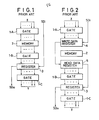
- Fig.1 is a block diagram showing the principles of a conventional logical unit.
- Reference numerals 1-A to 1-C indicate gates; 2 designates a memory; 3 identifies a register; SDi denotes scan-in data; SDo represents scan-out data ; X shows input data to the gate 1-A; and Y refers to output data from the gate 1-C.
- the gates 1-A to 1-C are not mere gates but are combinational circuits, such as arithmetic circuits or the like. The combinational circuit is diagnosed by checking its input and output data.
- the output data from the gate 1-A is input directly to the memory 2 and the input data to the gate 1-B is data read out directly from the memory 2.
- a scan function for the memory 2 is not provided; therefore, in the arrangement of Fig. 1, the gates 1-A and 1-B cannot be diagnosed individually.
- Fig. 2 is a block diagram showing the principles of another conventional logical unit which is provided with a write data register 4 and a read data register 5 in addition to the arrangement of Fig. 1.
- the input data X is provided thereto and its output is set in the write data register 4, after which data of the write data register 4 is read out therefrom by a serial scan operation.
- the gate 1-B data is written by a serial scan operation into the read data register 5 and its output data is input to the gate 1-B, the output data of which is set in the register 3. Then the data of the register 3 is read out therefrom by the serial scan operation. In this way, the gates 1-A and 1-B can be diagnosed.
- the write data register 4 and the read data register 5 are used during the diagnosis only and during normal operation, for speeding up the operation of the logical unit, they are by-passed so that the output data of the gate 1-A is input directly to the memory 2 and the read data of the memory 2 is input directly to the gate 1-B.
- the diagnostic ratio lowers unless an operation by the test pattern is not performed normally.
- an instruction for reference to the memory for instance, an instruction for adding data of first and second memories and storing the added data in the first memory , (MEM 1) ⁇ (MEM 1) + (MEM 2), is provided in an instruction register, the diagnostic results cannot be taken out to the outside. Therefore, when an instruction of the memory reference format is given, no diagnosis is possible. Accordingly, a high proportion of the memory reference instruction is a serious obstacle to diagnosis.
- the diagnostic system of the present invention is provided with a plurality of internal registers, an internal memory and a combinational circuit, such as an arithmetic unit, and at least one of the internal registers is arranged so that it can be scanned in and scanned out.
- the internal register that can be scanned in and scanned out is used in place of the internal memory.
- the present invention thus pertains to a diagnostic system which diagnoses a circuit referring to a memory through using an internal register.
- the present invention provides a diagnostic system which permits a diagnosis of a combinational circuit through using an internal register when a memory reference instruction is given during diagnosis.
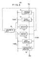
- an instruction decoded by the instruction register 15 is (MEM 1) + (MEM 1) + (DR), that is, an arithmetic instruction that adds the contents of the memory 11-1 and the data register 14 and sets the added data in the memory 11-1
- the contents of the memory 11-1 and the data register 14 are input into the arithmetic unit 16 via X and Y buses, respectively.
- the arithmetic results of the arithmetic unit 16 are written in the memory 11-1 via the Z bus. Further, each bit of the flag register 13 is set according to the arithmetic results.
- TM "1" and request signals to the memories are all inhibited but instead request signals to the flag register 13 and the data register 14 which are used an substitutes for the memories are valid.
- diagnosis a test pattern is set by a scan operation for each register.
- Fig. 4 is a block diagram illustrating the principal part of the embodiment of the present invention.
- Reference numeral 20 indicates a register (corresponding to the flag register 13 or data register 14 in Fig. 3); 21 designates a memory (corresponding to the memory 11-1 or 11-2 in Fig. 3); 22 and 23 identify OR circuits; 24 to 29 denote AND circuits; and A 0 to An, B 0 to B n , C 0 to C n and D 0 to D n represent gate groups, respectively.
- the gates B 0 to B n and D 0 to D n tristate gates are used for preventing a bus fight on the X and Y buses.
- Input data from the Z bus (see Fig. 3) to the register 20 is controlled by the gates A0 to An and output data from the register 20 to the X or Y bus (see Fig. 3) is controlled by the gates B 0 to B n .
- a control signal X for the gates A 0 to A n is made valid when the register write enable signal or the memory write enable signal in a test mode becomes valid.
- a control signal X 2 for the gates B 0 to B n is made valid when the register select signal or the memory select signal in the test mode becomes valid.
- Input data to the memory 21 is gated by the gates C o to C n and output data from the memory 21 is gated by the gates D 0 to D n .
- a control signal X 3 for the gates C 0 to C n is made valid by the memory write enable signal except in the test mode.
- a control signal X 4 for the gates D 0 to D n is made valid when the memory select signal except in the test mode becomes valid.
- the test mode signal When the system is in its normal operative state, the test mode signal is a "0", so that only the register write enable signal and the register select signal become valid for the register 20. And, if the scan mode signal happens to be a "0", the system clock is applied to the register 20 and when the register write enable signal is applied, the input data is set in the register 20. When the scan mode signal happens to be a "1”, the scan clock is provided to the register 20 and the scan-in data SDi is scanned in the register 20 and, at the same time, the scan-out data SDo is output therefrom. For the memory 21, too, the memory write enable signal and the memory select signal become valid. Consequently, the register 20 and the memory 21 are able to perform normal operation.
- the memory write enable signal becomes the control signal X 1 for the gates A 0 to An, whereas the memory select signal becomes the control signal X 2 for the gates B 0 to B n . Since the AND circuits 26 and 27 are closed, the control signals X 3 and X 4 for the gates C o to C n and D 0 to D n both go to "Os" and the memory 21 is separated by the gates C o to C n and D 0 to D n . In consequence, when a memory write instruction is executed, write data is set in the register 20 and when a memory read instruction is executed, the content of the register 20 is output.
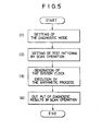
- Fig. 5 is a flowchart of the diagnostic operation, showing steps (1) to (4).
- Fig. 6 is a timing chart of the diagnostic operation.
- a device to be diagnosed assumes the following four states according to the test mode signal TM and the scan mode signal SM.
- the status of a register or a flip-flop in the device can be taken out to the outside, or they can be set to a desired state.
- the interior of the device is arranged for diagnosis.
- a control circuit for preventing a bus fight during diagnosis and the diagnostic function for the memory in the device become valid under this condition.
- the scan in/scan out is performed under the diagnostic condition. That is, a test pattern for diagnosis is set and the diagnostic results are taken out.
- the period during which the scan mode signal remains at the "0" level is the period for execution of one instruction and when the scan mode signal goes to the "1" level again, the scan clock is provided to the register 20, scanning out its content.
- This scan-out data SDo is taken out to the outside for diagnosing the combinational circuit, such as an arithmetic unit.
Landscapes
- Engineering & Computer Science (AREA)
- General Engineering & Computer Science (AREA)
- Theoretical Computer Science (AREA)
- Computer Hardware Design (AREA)
- Quality & Reliability (AREA)
- Physics & Mathematics (AREA)
- General Physics & Mathematics (AREA)
- Test And Diagnosis Of Digital Computers (AREA)
- Tests Of Electronic Circuits (AREA)
Applications Claiming Priority (2)
| Application Number | Priority Date | Filing Date | Title |
|---|---|---|---|
| JP57028642A JPS58144954A (ja) | 1982-02-24 | 1982-02-24 | 診断方式 |
| JP28642/82 | 1982-02-24 |
Publications (3)
| Publication Number | Publication Date |
|---|---|
| EP0087314A2 true EP0087314A2 (fr) | 1983-08-31 |
| EP0087314A3 EP0087314A3 (en) | 1985-07-31 |
| EP0087314B1 EP0087314B1 (fr) | 1989-04-19 |
Family
ID=12254170
Family Applications (1)
| Application Number | Title | Priority Date | Filing Date |
|---|---|---|---|
| EP19830300907 Expired EP0087314B1 (fr) | 1982-02-24 | 1983-02-22 | Système de diagnostic dans un processeur de données |
Country Status (4)
| Country | Link |
|---|---|
| EP (1) | EP0087314B1 (fr) |
| JP (1) | JPS58144954A (fr) |
| DE (1) | DE3379688D1 (fr) |
| ES (1) | ES519977A0 (fr) |
Cited By (2)
| Publication number | Priority date | Publication date | Assignee | Title |
|---|---|---|---|---|
| EP0377455A3 (fr) * | 1989-01-06 | 1991-10-23 | SHARP Corporation | Système de commutation dans le mode de test pour LSI |
| EP0416532A3 (en) * | 1989-09-07 | 1992-06-24 | Nec Corporation | Semiconductor memory device associated with peripheral logic gates having a scan-path diagnostic mode of operation |
Family Cites Families (4)
| Publication number | Priority date | Publication date | Assignee | Title |
|---|---|---|---|---|
| JPS5833576B2 (ja) * | 1977-03-14 | 1983-07-20 | 株式会社東芝 | 計算機システムの故障診断装置 |
| JPS5939052B2 (ja) * | 1977-03-15 | 1984-09-20 | 株式会社東芝 | 情報処理装置及び方法 |
| US4223382A (en) * | 1978-11-30 | 1980-09-16 | Sperry Corporation | Closed loop error correct |
| JPS55150047A (en) * | 1979-05-10 | 1980-11-21 | Nec Corp | Test unit for information processor |
-
1982
- 1982-02-24 JP JP57028642A patent/JPS58144954A/ja active Granted
-
1983
- 1983-02-22 DE DE8383300907T patent/DE3379688D1/de not_active Expired
- 1983-02-22 ES ES519977A patent/ES519977A0/es active Granted
- 1983-02-22 EP EP19830300907 patent/EP0087314B1/fr not_active Expired
Cited By (3)
| Publication number | Priority date | Publication date | Assignee | Title |
|---|---|---|---|---|
| EP0377455A3 (fr) * | 1989-01-06 | 1991-10-23 | SHARP Corporation | Système de commutation dans le mode de test pour LSI |
| US5144627A (en) * | 1989-01-06 | 1992-09-01 | Sharp Kabushiki Kaisha | Test mode switching system for lsi |
| EP0416532A3 (en) * | 1989-09-07 | 1992-06-24 | Nec Corporation | Semiconductor memory device associated with peripheral logic gates having a scan-path diagnostic mode of operation |
Also Published As
| Publication number | Publication date |
|---|---|
| ES8402967A1 (es) | 1984-03-01 |
| ES519977A0 (es) | 1984-03-01 |
| DE3379688D1 (en) | 1989-05-24 |
| JPS6246021B2 (fr) | 1987-09-30 |
| JPS58144954A (ja) | 1983-08-29 |
| EP0087314B1 (fr) | 1989-04-19 |
| EP0087314A3 (en) | 1985-07-31 |
Similar Documents
| Publication | Publication Date | Title |
|---|---|---|
| US4937770A (en) | Simulation system | |
| US5056013A (en) | In-circuit emulator | |
| JPH05108396A (ja) | プロセツサ回路 | |
| EP0109770A2 (fr) | Essai des circuits électroniques digitaux | |
| JPS60175152A (ja) | 浮動小数点加速プロセツサの自己試験のための方法及び装置 | |
| EP0261497A2 (fr) | Circuit sémaphore pour cellules de mémoire partagées | |
| US4876645A (en) | Diagnostic system | |
| US5872954A (en) | Method of monitoring registers during emulation | |
| EP0087314A2 (fr) | Système de diagnostic dans un processeur de données | |
| JPS6226734B2 (fr) | ||
| EP0463352B1 (fr) | Microprocesseur pour émulateur interne au circuit avec espace d'usager et espace d'émulateur interne au circuit séparé | |
| Bayliss et al. | The interface processor for the Intel VLSI 432 32-bit computer | |
| EP0173257B1 (fr) | Dispositif de circuit intégré | |
| EP0231948A2 (fr) | Système de simulation | |
| JP2533170Y2 (ja) | 診断デ−タ取込み装置 | |
| JPH07110790A (ja) | メモリ診断装置 | |
| JPH01263739A (ja) | 情報処理装置 | |
| JPH05334116A (ja) | デバッグ制御方式 | |
| JP2935710B2 (ja) | プロセッサ集積回路装置のテスト装置 | |
| JPS6136659B2 (fr) | ||
| JPH03105431A (ja) | 大規模集積回路の故障診断方法 | |
| JPS6327735B2 (fr) | ||
| JPH039438A (ja) | 診断用回路 | |
| JPH07120535A (ja) | 論理回路の診断方法およびlsi回路 | |
| JPH1165872A (ja) | ビルトインセルフテスト回路を備えた処理装置 |
Legal Events
| Date | Code | Title | Description |
|---|---|---|---|
| PUAI | Public reference made under article 153(3) epc to a published international application that has entered the european phase |
Free format text: ORIGINAL CODE: 0009012 |
|
| AK | Designated contracting states |
Designated state(s): DE FR GB |
|
| PUAL | Search report despatched |
Free format text: ORIGINAL CODE: 0009013 |
|
| AK | Designated contracting states |
Designated state(s): DE FR GB |
|
| 17P | Request for examination filed |
Effective date: 19851125 |
|
| 17Q | First examination report despatched |
Effective date: 19870203 |
|
| GRAA | (expected) grant |
Free format text: ORIGINAL CODE: 0009210 |
|
| AK | Designated contracting states |
Kind code of ref document: B1 Designated state(s): DE FR GB |
|
| REF | Corresponds to: |
Ref document number: 3379688 Country of ref document: DE Date of ref document: 19890524 |
|
| ET | Fr: translation filed | ||
| PGFP | Annual fee paid to national office [announced via postgrant information from national office to epo] |
Ref country code: GB Payment date: 19900131 Year of fee payment: 8 |
|
| PLBE | No opposition filed within time limit |
Free format text: ORIGINAL CODE: 0009261 |
|
| STAA | Information on the status of an ep patent application or granted ep patent |
Free format text: STATUS: NO OPPOSITION FILED WITHIN TIME LIMIT |
|
| PGFP | Annual fee paid to national office [announced via postgrant information from national office to epo] |
Ref country code: DE Payment date: 19900219 Year of fee payment: 8 |
|
| 26N | No opposition filed | ||
| PGFP | Annual fee paid to national office [announced via postgrant information from national office to epo] |
Ref country code: FR Payment date: 19901228 Year of fee payment: 9 |
|
| PG25 | Lapsed in a contracting state [announced via postgrant information from national office to epo] |
Ref country code: GB Effective date: 19910222 |
|
| GBPC | Gb: european patent ceased through non-payment of renewal fee | ||
| PG25 | Lapsed in a contracting state [announced via postgrant information from national office to epo] |
Ref country code: DE Effective date: 19911101 |
|
| PG25 | Lapsed in a contracting state [announced via postgrant information from national office to epo] |
Ref country code: FR Effective date: 19921030 |
|
| REG | Reference to a national code |
Ref country code: FR Ref legal event code: ST |