EP0088126B2 - Eingebetteter flüssigkristall und verfahren - Google Patents
Eingebetteter flüssigkristall und verfahren Download PDFInfo
- Publication number
- EP0088126B2 EP0088126B2 EP82903099A EP82903099A EP0088126B2 EP 0088126 B2 EP0088126 B2 EP 0088126B2 EP 82903099 A EP82903099 A EP 82903099A EP 82903099 A EP82903099 A EP 82903099A EP 0088126 B2 EP0088126 B2 EP 0088126B2
- Authority
- EP
- European Patent Office
- Prior art keywords
- liquid crystal
- crystal material
- encapsulated
- electric field
- containment means
- Prior art date
- Legal status (The legal status is an assumption and is not a legal conclusion. Google has not performed a legal analysis and makes no representation as to the accuracy of the status listed.)
- Expired - Lifetime
Links
- 239000004973 liquid crystal related substance Substances 0.000 title claims abstract description 363
- 238000000034 method Methods 0.000 title claims abstract description 16
- 239000000463 material Substances 0.000 claims abstract description 248
- 239000002775 capsule Substances 0.000 claims description 95
- 230000005684 electric field Effects 0.000 claims description 68
- 239000000758 substrate Substances 0.000 claims description 39
- 230000003287 optical effect Effects 0.000 claims description 26
- 239000004372 Polyvinyl alcohol Substances 0.000 claims description 19
- 229920002451 polyvinyl alcohol Polymers 0.000 claims description 19
- 230000004044 response Effects 0.000 claims description 14
- 239000004988 Nematic liquid crystal Substances 0.000 claims description 13
- 238000004519 manufacturing process Methods 0.000 claims description 9
- 238000010521 absorption reaction Methods 0.000 claims description 5
- 229920000642 polymer Polymers 0.000 claims description 5
- 239000011347 resin Substances 0.000 claims description 5
- 229920005989 resin Polymers 0.000 claims description 5
- 108010010803 Gelatin Proteins 0.000 claims description 2
- 229920000159 gelatin Polymers 0.000 claims description 2
- 239000008273 gelatin Substances 0.000 claims description 2
- 235000019322 gelatine Nutrition 0.000 claims description 2
- 235000011852 gelatine desserts Nutrition 0.000 claims description 2
- 230000002829 reductive effect Effects 0.000 claims description 2
- FPYJFEHAWHCUMM-UHFFFAOYSA-N maleic anhydride Chemical compound O=C1OC(=O)C=C1 FPYJFEHAWHCUMM-UHFFFAOYSA-N 0.000 claims 2
- NIXOWILDQLNWCW-UHFFFAOYSA-N Acrylic acid Chemical group OC(=O)C=C NIXOWILDQLNWCW-UHFFFAOYSA-N 0.000 claims 1
- 229940096529 carboxypolymethylene Drugs 0.000 claims 1
- 229920001577 copolymer Polymers 0.000 claims 1
- 230000001939 inductive effect Effects 0.000 claims 1
- 230000031700 light absorption Effects 0.000 claims 1
- XJRBAMWJDBPFIM-UHFFFAOYSA-N methyl vinyl ether Chemical compound COC=C XJRBAMWJDBPFIM-UHFFFAOYSA-N 0.000 claims 1
- 230000000007 visual effect Effects 0.000 abstract description 6
- 239000000975 dye Substances 0.000 description 39
- 239000010410 layer Substances 0.000 description 32
- 239000003990 capacitor Substances 0.000 description 14
- 230000000694 effects Effects 0.000 description 13
- 239000000839 emulsion Substances 0.000 description 10
- 230000005540 biological transmission Effects 0.000 description 9
- 230000010287 polarization Effects 0.000 description 8
- XLYOFNOQVPJJNP-UHFFFAOYSA-N water Substances O XLYOFNOQVPJJNP-UHFFFAOYSA-N 0.000 description 8
- 229920002799 BoPET Polymers 0.000 description 5
- 239000005041 Mylar™ Substances 0.000 description 5
- 230000003098 cholesteric effect Effects 0.000 description 5
- 238000000576 coating method Methods 0.000 description 5
- 239000004615 ingredient Substances 0.000 description 5
- 239000011253 protective coating Substances 0.000 description 5
- 239000011248 coating agent Substances 0.000 description 4
- 239000007788 liquid Substances 0.000 description 4
- GWEVSGVZZGPLCZ-UHFFFAOYSA-N Titan oxide Chemical compound O=[Ti]=O GWEVSGVZZGPLCZ-UHFFFAOYSA-N 0.000 description 3
- 239000000084 colloidal system Substances 0.000 description 3
- 239000007772 electrode material Substances 0.000 description 3
- 238000005538 encapsulation Methods 0.000 description 3
- 230000005284 excitation Effects 0.000 description 3
- 239000011521 glass Substances 0.000 description 3
- 229910052738 indium Inorganic materials 0.000 description 3
- APFVFJFRJDLVQX-UHFFFAOYSA-N indium atom Chemical compound [In] APFVFJFRJDLVQX-UHFFFAOYSA-N 0.000 description 3
- 230000002441 reversible effect Effects 0.000 description 3
- 239000000126 substance Substances 0.000 description 3
- OGIDPMRJRNCKJF-UHFFFAOYSA-N titanium oxide Inorganic materials [Ti]=O OGIDPMRJRNCKJF-UHFFFAOYSA-N 0.000 description 3
- 239000004986 Cholesteric liquid crystals (ChLC) Substances 0.000 description 2
- 239000004990 Smectic liquid crystal Substances 0.000 description 2
- 230000008901 benefit Effects 0.000 description 2
- 230000015572 biosynthetic process Effects 0.000 description 2
- 238000010586 diagram Methods 0.000 description 2
- 230000014759 maintenance of location Effects 0.000 description 2
- 239000002245 particle Substances 0.000 description 2
- 230000000704 physical effect Effects 0.000 description 2
- 238000007639 printing Methods 0.000 description 2
- 230000008569 process Effects 0.000 description 2
- 150000003839 salts Chemical class 0.000 description 2
- 230000035945 sensitivity Effects 0.000 description 2
- YCUVUDODLRLVIC-VPHDGDOJSA-N sudan black b Chemical compound C1=CC(=C23)NC(C)(C)NC2=CC=CC3=C1\N=N\C(C1=CC=CC=C11)=CC=C1\N=N\C1=CC=CC=C1 YCUVUDODLRLVIC-VPHDGDOJSA-N 0.000 description 2
- 238000009736 wetting Methods 0.000 description 2
- VRZJGENLTNRAIG-UHFFFAOYSA-N 4-[4-(dimethylamino)phenyl]iminonaphthalen-1-one Chemical compound C1=CC(N(C)C)=CC=C1N=C1C2=CC=CC=C2C(=O)C=C1 VRZJGENLTNRAIG-UHFFFAOYSA-N 0.000 description 1
- LFQSCWFLJHTTHZ-UHFFFAOYSA-N Ethanol Chemical compound CCO LFQSCWFLJHTTHZ-UHFFFAOYSA-N 0.000 description 1
- FHNINJWBTRXEBC-UHFFFAOYSA-N Sudan III Chemical compound OC1=CC=C2C=CC=CC2=C1N=NC(C=C1)=CC=C1N=NC1=CC=CC=C1 FHNINJWBTRXEBC-UHFFFAOYSA-N 0.000 description 1
- 125000003118 aryl group Chemical group 0.000 description 1
- 230000008859 change Effects 0.000 description 1
- JBTHDAVBDKKSRW-UHFFFAOYSA-N chembl1552233 Chemical compound CC1=CC(C)=CC=C1N=NC1=C(O)C=CC2=CC=CC=C12 JBTHDAVBDKKSRW-UHFFFAOYSA-N 0.000 description 1
- 230000008878 coupling Effects 0.000 description 1
- 238000010168 coupling process Methods 0.000 description 1
- 238000005859 coupling reaction Methods 0.000 description 1
- 239000013078 crystal Substances 0.000 description 1
- 230000007423 decrease Effects 0.000 description 1
- 230000006866 deterioration Effects 0.000 description 1
- 238000004033 diameter control Methods 0.000 description 1
- 239000003989 dielectric material Substances 0.000 description 1
- 238000009826 distribution Methods 0.000 description 1
- 238000001035 drying Methods 0.000 description 1
- 230000005685 electric field effect Effects 0.000 description 1
- 239000003995 emulsifying agent Substances 0.000 description 1
- 150000002148 esters Chemical class 0.000 description 1
- 238000001704 evaporation Methods 0.000 description 1
- 230000008020 evaporation Effects 0.000 description 1
- UPBDXRPQPOWRKR-UHFFFAOYSA-N furan-2,5-dione;methoxyethene Chemical compound COC=C.O=C1OC(=O)C=C1 UPBDXRPQPOWRKR-UHFFFAOYSA-N 0.000 description 1
- 230000003993 interaction Effects 0.000 description 1
- 230000000670 limiting effect Effects 0.000 description 1
- 239000011159 matrix material Substances 0.000 description 1
- 239000000203 mixture Substances 0.000 description 1
- 230000003647 oxidation Effects 0.000 description 1
- 238000007254 oxidation reaction Methods 0.000 description 1
- 230000036961 partial effect Effects 0.000 description 1
- 229920003023 plastic Polymers 0.000 description 1
- 239000004033 plastic Substances 0.000 description 1
- 239000002985 plastic film Substances 0.000 description 1
- 229920000867 polyelectrolyte Polymers 0.000 description 1
- 239000002244 precipitate Substances 0.000 description 1
- 230000001681 protective effect Effects 0.000 description 1
- 239000011241 protective layer Substances 0.000 description 1
- 230000006903 response to temperature Effects 0.000 description 1
- 230000004043 responsiveness Effects 0.000 description 1
- 238000010020 roller printing Methods 0.000 description 1
- 230000037390 scarring Effects 0.000 description 1
- 238000000926 separation method Methods 0.000 description 1
- 239000002356 single layer Substances 0.000 description 1
- 238000004544 sputter deposition Methods 0.000 description 1
- 239000000725 suspension Substances 0.000 description 1
- XOLBLPGZBRYERU-UHFFFAOYSA-N tin dioxide Chemical compound O=[Sn]=O XOLBLPGZBRYERU-UHFFFAOYSA-N 0.000 description 1
- 229910001887 tin oxide Inorganic materials 0.000 description 1
- 238000001771 vacuum deposition Methods 0.000 description 1
- 239000000080 wetting agent Substances 0.000 description 1
Images
Classifications
-
- G—PHYSICS
- G02—OPTICS
- G02F—OPTICAL DEVICES OR ARRANGEMENTS FOR THE CONTROL OF LIGHT BY MODIFICATION OF THE OPTICAL PROPERTIES OF THE MEDIA OF THE ELEMENTS INVOLVED THEREIN; NON-LINEAR OPTICS; FREQUENCY-CHANGING OF LIGHT; OPTICAL LOGIC ELEMENTS; OPTICAL ANALOGUE/DIGITAL CONVERTERS
- G02F1/00—Devices or arrangements for the control of the intensity, colour, phase, polarisation or direction of light arriving from an independent light source, e.g. switching, gating or modulating; Non-linear optics
- G02F1/01—Devices or arrangements for the control of the intensity, colour, phase, polarisation or direction of light arriving from an independent light source, e.g. switching, gating or modulating; Non-linear optics for the control of the intensity, phase, polarisation or colour
- G02F1/13—Devices or arrangements for the control of the intensity, colour, phase, polarisation or direction of light arriving from an independent light source, e.g. switching, gating or modulating; Non-linear optics for the control of the intensity, phase, polarisation or colour based on liquid crystals, e.g. single liquid crystal display cells
- G02F1/133—Constructional arrangements; Operation of liquid crystal cells; Circuit arrangements
- G02F1/1333—Constructional arrangements; Manufacturing methods
- G02F1/1335—Structural association of cells with optical devices, e.g. polarisers or reflectors
-
- C—CHEMISTRY; METALLURGY
- C09—DYES; PAINTS; POLISHES; NATURAL RESINS; ADHESIVES; COMPOSITIONS NOT OTHERWISE PROVIDED FOR; APPLICATIONS OF MATERIALS NOT OTHERWISE PROVIDED FOR
- C09K—MATERIALS FOR MISCELLANEOUS APPLICATIONS, NOT PROVIDED FOR ELSEWHERE
- C09K19/00—Liquid crystal materials
- C09K19/52—Liquid crystal materials characterised by components which are not liquid crystals, e.g. additives with special physical aspect: solvents, solid particles
- C09K19/54—Additives having no specific mesophase characterised by their chemical composition
- C09K19/542—Macromolecular compounds
- C09K19/544—Macromolecular compounds as dispersing or encapsulating medium around the liquid crystal
-
- G—PHYSICS
- G02—OPTICS
- G02F—OPTICAL DEVICES OR ARRANGEMENTS FOR THE CONTROL OF LIGHT BY MODIFICATION OF THE OPTICAL PROPERTIES OF THE MEDIA OF THE ELEMENTS INVOLVED THEREIN; NON-LINEAR OPTICS; FREQUENCY-CHANGING OF LIGHT; OPTICAL LOGIC ELEMENTS; OPTICAL ANALOGUE/DIGITAL CONVERTERS
- G02F1/00—Devices or arrangements for the control of the intensity, colour, phase, polarisation or direction of light arriving from an independent light source, e.g. switching, gating or modulating; Non-linear optics
- G02F1/01—Devices or arrangements for the control of the intensity, colour, phase, polarisation or direction of light arriving from an independent light source, e.g. switching, gating or modulating; Non-linear optics for the control of the intensity, phase, polarisation or colour
- G02F1/13—Devices or arrangements for the control of the intensity, colour, phase, polarisation or direction of light arriving from an independent light source, e.g. switching, gating or modulating; Non-linear optics for the control of the intensity, phase, polarisation or colour based on liquid crystals, e.g. single liquid crystal display cells
- G02F1/133—Constructional arrangements; Operation of liquid crystal cells; Circuit arrangements
- G02F1/1333—Constructional arrangements; Manufacturing methods
- G02F1/1334—Constructional arrangements; Manufacturing methods based on polymer dispersed liquid crystals, e.g. microencapsulated liquid crystals
-
- G—PHYSICS
- G02—OPTICS
- G02F—OPTICAL DEVICES OR ARRANGEMENTS FOR THE CONTROL OF LIGHT BY MODIFICATION OF THE OPTICAL PROPERTIES OF THE MEDIA OF THE ELEMENTS INVOLVED THEREIN; NON-LINEAR OPTICS; FREQUENCY-CHANGING OF LIGHT; OPTICAL LOGIC ELEMENTS; OPTICAL ANALOGUE/DIGITAL CONVERTERS
- G02F1/00—Devices or arrangements for the control of the intensity, colour, phase, polarisation or direction of light arriving from an independent light source, e.g. switching, gating or modulating; Non-linear optics
- G02F1/01—Devices or arrangements for the control of the intensity, colour, phase, polarisation or direction of light arriving from an independent light source, e.g. switching, gating or modulating; Non-linear optics for the control of the intensity, phase, polarisation or colour
- G02F1/13—Devices or arrangements for the control of the intensity, colour, phase, polarisation or direction of light arriving from an independent light source, e.g. switching, gating or modulating; Non-linear optics for the control of the intensity, phase, polarisation or colour based on liquid crystals, e.g. single liquid crystal display cells
- G02F1/137—Devices or arrangements for the control of the intensity, colour, phase, polarisation or direction of light arriving from an independent light source, e.g. switching, gating or modulating; Non-linear optics for the control of the intensity, phase, polarisation or colour based on liquid crystals, e.g. single liquid crystal display cells characterised by the electro-optical or magneto-optical effect, e.g. field-induced phase transition, orientation effect, guest-host interaction or dynamic scattering
-
- G—PHYSICS
- G02—OPTICS
- G02F—OPTICAL DEVICES OR ARRANGEMENTS FOR THE CONTROL OF LIGHT BY MODIFICATION OF THE OPTICAL PROPERTIES OF THE MEDIA OF THE ELEMENTS INVOLVED THEREIN; NON-LINEAR OPTICS; FREQUENCY-CHANGING OF LIGHT; OPTICAL LOGIC ELEMENTS; OPTICAL ANALOGUE/DIGITAL CONVERTERS
- G02F2202/00—Materials and properties
- G02F2202/04—Materials and properties dye
- G02F2202/043—Materials and properties dye pleochroic
Definitions
- the present invention relates generally to devices incorporating liquid crystals and, more particularly, to devices incorporating liquid crystal material and containment means therefor. Moreover, the invention relates to devices using encapsulated liquid crystals and to methods of making encapsulated liquid crystals.
- Liquid crystals currently are used in a wide variety of devices, including optical devices such as visual displays. Such devices usually require relatively low power and have satisfactory response time, provide reasonable contrast, and are relatively economical.
- the property of liquid crystals enabling use, for example, in visual displays, is the ability of liquid crystals to transmit light on one hand, and to scatter light and/or to absorb light, on the other, in dependence on whether the liquid crystals are in a relatively free, i.e. deenergized or field off state or in a strictly aligned, i.e. an energized or field on state, e.g. with an electric field applied across the liquid crystal material.
- An example of electrically responsive liquid crystal material and use thereof is provided in U.S. Patent 3,322,485.
- Certain liquid crystal material is responsive to temperature, changing optical characteristics in response to temperature of the liquid crystal material.
- liquid crystal materials there are three categories of liquid crystal materials, namely cholesteric, nematic and smectic types.
- the invention of the present application relates in a preferred embodiment described below to use of nematic liquid crystal material or to a combination of nematic and some cholesteric type.
- various principles of the invention may be employed with various one or ones of the known types of liquid crystal material or combinations thereof.
- the various characteristics of the cholesteric, nematic and smectic types of liquid crystal material are described in the prior art.
- One known characteristic of liquid crystal material is that of reversibility; in particular it is noted here that nematic liquid crystal material is known to be reversible, but cholosteric material is not reversible.
- pleochroic dyes have been mixed with the liquid crystal material to form a solution therewith.
- the molecules of pleochroic material generally align with the molecules of the liquid crystal material. Therefore, such pleochroic dyes will tend to function optically in a manner similar to that of the liquid crystal material in response to a changing parameter, such as application or non-application of an electric field. Examples of pleochroic dyes with liquid crystal material are described in U.S. Patents 3,499,702 and 3,551,026.
- liquid crystal material has different physical properties in different directions.
- liquid crystals may be optically anisotropic such that when the molecules are randomly oriented they permit light transmission and, when they are aligned due to application of an electric field thereacross, light may be transmitted through the liquid crystal material.
- Liquid crystal material also has electrical anisotropy.
- the dielectric constant for nematic liquid crystal material may be one value when the liquid crystal molecules are parallel to the electric field and may have a different value when the liquid crystal molecules are aligned perpendicular to an electric field. Since such dielectric value is a function of alignment, for example, reference to the same as a "dielectric coefficient" may be more apt than the usual "dielectric constant" label. Similar properties are true for other types of liquid crystals.
- liquid crystals such as visual display devices or other devices
- Large size devices using liquid crystals such as, for example, a billboard display or a sign have not been able to be made satisfactorily for a number of reasons.
- One reason is the fluidity of the liquid crystals, (the liquid crystal material may tend to flow creating areas of the display that have different thicknesses).
- the optical characteristics of the display may lack uniformity, have varying contrast characteristics at different portions of the display, etc.; the thickness variations cause variations or gradations in optical properties of the liquid crystal device.
- the varying thickness of the liquid crystal material will cause corresponding variations in the electrical properties of the liquid crystal material, such as capacitance and impedance, further reducing uniformity of a large size liquid crystal device.
- the varying electrical properties of the liquid crystal material also may cause a corresponding variation in the effective electric field applied across the liquid crystal material and/or in response to a constant electric field would respond differently at areas of the liquid crystal that are of different thicknesses.
- a pleochroic display i.e. one in which pleocroic dye and liquid crystal material are in solution, has the advantage of not requiring a polarizer.
- a pleochroic device has a disadvantage of relatively low contrast when used directly in the nematic form. It was discovered in the past, though, that a cholesteric liquid crystal material could be added to the nematic one together with the dye to improve the contrast ratio. See White et al article, "Journal ofApplied Physics", Volume 45, No. 11, November 1974, at pages 4718-4723, for example. The cholesteric material would tend not to return to its original zero field form when the electric field is removed.
- pleochroic dye included in solution with liquid crystal material regardless of the particular type of liquid crystal material, is that the absorbtion of the dye is not zero in the field-on condition; rather such absorbtion in the field-on condition follows a so-called ordering parameter, which relates to or is a function of the relative alignment of the dyes.
- the optical transmission characteristic of liquid crystal material is an exponential function of thickness of the liquid crystal material; specifically, the on state or field-on or energized state of the liquid crystal material is an exponential function of thickness of the liquid crystal material, and the absorbing state or off state also is a different exponential function of thickness.
- liquid crystal material should have an optimum uniform thickness.
- liquid crystal material means the liquid crystals themselves and, depending on context, a pleochroic dye in solution therewith.
- optimum thickness and spacing rather close tolerances must be maintained.
- there is a limit as to the size of the device using such liquid crystals for it is quite difficult to maintain close tolerances over large surface areas, for example.
- the invention provides two method of making encapsulated liquid crystal material according to Claims 23 and 24.
- the invention provides optical apparatus according to Claim 21.
- embodiments of the invention are particularly concerned with liquid crystal material and especially nematic material, which is encapsulated and used in liquid crystal devices, such as relatively large size display devices.
- liquid crystal material broadly refers to any type of liquid crystal material that will work in the context of the present invention, but preferably refers to nematic type. Such liquid crystal material also may include pleochroic dye or other ingredient.
- a capsule refers to a containment device or medium that confines a quantity of liquid crystal material, and encapsulating medium or material is that medium or material of which such capsules are formed.
- An encapsulated liquid crystal or encapsulated liquid crystal material means a quantity of liquid crystal material confined or contained in the encapsulating medium, such as the noted capsules.
- a liquid crystal device is a device formed of liquid crystal material, in the present invention such devices are formed of encapsulated liquid crystals capable of providing a function of the type typically inuring to liquid crystal material; for example, such a liquid crystal device may be a visual display that in response to application and removal of an electric field effects a selected attenuation of visible light.
- One method of making encapsulated liquid crystals includes mixing together liquid crystal material and an encapsulating medium in which the liquid crystal material will not dissolve and permitting formation of discrete capsules containing the liquid crystal material.
- a method of making a liquid crystal device including such encapsulated liquid crystal includes, for example applying such encapsulated liquid crystal material to a substrate. Moreover, such a method may include providing means for applying an electric field to the liquid crystal material to affect a property thereof.
- a nematic material with positive dielectric anisotropy in which may be dissolved a pleochroic dye is placed in a generally spherical capsule.
- the capsule wall distorts the liquid crystal molecules so they and the dye when no field is applied will tend to absorb all directions of polarized light.
- a suitable electric field is applied across such a capsule, for example across an axis thereof, the liquid crystal material will tend to align parallel to such field causing the absorbtion characteristics of such material to be reduced to one assumed when the liquid crystal material is in planar configuration.
- the encapsulating material may have a dielectric constant near to that of the liquid crystal material, on the one hand, and a relatively large impedance, on the other hand, and the liquid crystal material itself may have a positive dielectric anisotropy.
- Contrast of a liquid crystal device employing encapsulated liquid crystals may be improved by selecting an encapsulating medium that has an index of refraction that is matched to the ordinary index of refraction of the liquid crystal material.
- the encapsulating medium may be used not only to encapsulate liquid crystal material but also to adhere the capsules to a substrate for support thereon.
- a further binding medium may be used to hold the liquid crystal capsules relative to a substrate.
- the additional binding medium has an index of refraction which is matched to that of the encapsulating medium for maintaining the improved contrast characteristic described above.
- a feature of the spherical or otherwise curved capsule which confines the liquid crystal material therein in accordance with embodiments of the present invention is that the liquid crystal material tends to follow the curvature or otherwise to align generally parallel with the curved surfaces of such capsule. Accordingly, the individual liquid crystal molecules tend to be forced or distorted to a specific form, being folded back on themselves in a sense as they follow the capsule wall, so that the resulting optical characteristic of a given capsule containing liquid crystal material is such that substantially all light delivered thereto will be absorbed when no electric field is applied, regardless of the polarization direction of the incident light. Even without dye this effect causes scattering and thus opacity.
- Another feature is the ability to control the effective thickness of the liquid crystal material contained in a capsule by controlling the internal diameter of such capsule.
- Such diameter control may be effected by a separation process during the method of making the encapsulated liquid crystals using any one of a variety of conventional or novel sorting techniques as well as by controlling the mixing process, the quantities of ingredients, and/or the nature of the ingredients provided during mixing.
- a further and very significant feature of the present invention is that there appears to be no limitation on the size of a high quality liquid crystal device that can be made using the encapsulated liquid crystals in accordance with the present invention. More specifically, by providing confinement for discrete quantities of liquid crystal material, for example, in the described capsules, the various problems encountered in the past that prevented use of liquid crystal material in large size devices are overcome, for each individual capsule in effect can still operate as an independent liquid crystal device. Moreover, each capsule, then, preferably has physical properties enabling it to be mounted in virtually any environment including one containing a plurality of further such liquid crystal capsules mounted to a substrate or otherwise supported for use in response to application and removal of some type of excitation source, such as, for example, an electric field or the like.
- an encapsulating medium having electrical properties matched in a prescribed way to the electrical properties of liquid crystal material encapsulated thereby and additionally preferably optically matched to optical properties of such liquid crystal material permits efficient and high quality functioning of the liquid crystal material in response to excitation or non-excitation by an external source; and that the interaction of the encapsulating medium with the liquid crystal material distorts the latter in a prescribed manner changing an operational mode of liquid crystal material.
- the liquid crystals will absorb or block, rather than transmit, light when not subject to an electric field and will be functional with respect to all manners of incident light regardless of the direction of polarization of such incident light.
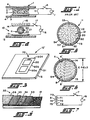
- prior art liquid crystal device is generally indicated at 1.
- Such device 1 includes liquid crystal material 2 sandwiched between electrodes 3 of, for example, indium doped titanium oxide that are deposited for support on respective mounting or confining substrates 4, such as glass, plastic sheets or the like.
- the sheets 4 may be clear as may be the electrodes 3 so that the device 1 is an optical transmission control device, whereby incident light may be scattered when no electric field is applied by the electrodes 3 across a liquid crystal material 2 and the incident light may be transmitted through the liquid crystal material 2 when an electric field is applied thereacross.
- Electric leads 5 and switch 6 selectively couple voltage source 7 across the electrodes 3 to provide such electric field.
- the voltage source 7 may be either an AC or a DC voltage source.
- the liquid crystal material 2, and specifically the individual molecules thereof, in the device 1 are somewhat confined by the substrates 4 for retention in a desired location, say for example, to be used overall as part of a digital display device.
- the liquid crystal material 2, and specifically the individual molecules thereof must have adequate freedom of movement so that they may assume either a random orientation or distribution when no electric field is applied or a prescribed distributional or orien- tational alignment when an electric field is applied across the electrodes 3.
- one of the substrates 4 may be reflective to reflect incident light received through the liquid crystal material 2 back through the latter for delivery through the other substrate 4 for subsequent use.
- the liquid crystal material 2 may be of virtually any type that is responsive to an electric field applied thereacross so as to have a desired operating characteristic intended for the device 1; the liquid crystal material 2 also may include, if desired, pleochroic dye material in solution therewith.
- the device 10 includes an encapsulated liquid crystal 11 which is supported from a mounting substrate 12 across which an electric field may be applied via electrodes 13, 14.
- the electrode of 13 may be, for example, a quantity vacuum deposited indium doped titanium oxide applied to the substrate 12, and the electrode 14 may be, for example, electrically conductive ink.
- a protective layer or coating 15 may be applied over the electrode 14 for protective purposes but such layer 15 or- d inarily would not be necessary for supporting or confining the encapsulated liquid crystal 11 or the electrode 14.
- Voltage may be applied to the electrodes 13, 14 from an AC or DC voltage source 16, selectively closable switch 17, and electrical leads 18,19 in turn to apply an electric field across the encapsulated liquid crystal 11 when the switch 17 is closed.
- the encapsulated liquid crystal 11 includes liquid crystal material 20 contained within the confines or in- teriorvolume 21 of a capsule 22.
- the capsule 22 is generally spherical.
- the principles of the invention would apply when the capsule 22 is of a shape other than spherical; such shape should provide the desired optical and electrical characteristics that will satisfactorily coexist with the optical characteristics of the liquid crystal 20, e.g. index of refraction, and will permit an adequate portion of the electric field to occur across the liquid crystal material 20 itself for effecting desired alignment of the liquid crystal molecules when it is desired to have a field on condition.
- a particular advantage to the preferred spherical configuration of the capsule 22 will be described below with respect to the distortion it effects on the liquid crystal molecules.
- the mounting substrate 12 and the electrodes 13,14 as well as the protective coating 15 may be optically transmissive so that the liquid crystal device 10 is capable of controlling transmission of light therethrough in response to whether or not an electric field is applied across the electrodes 13, 14 and, thus, across the encapsulated liquid crystal 11.
- the mounting substrate 12 may be optically reflective or may have thereon an optically reflective coating so that reflection by such reflective coating of incident light received through the protective coating 15 will be a function of whether or not there is an electric field applied across the encapsulated liquid crystal 11.
- a plurality of encapsulated liquid crystals 11 would be applied to the mounting substrate 12 in a manner such that the encapsulated liquid crystals adhere to the mounting substrate 12 orto an interface material, such as the electrode 13, for support by the mounting substrate 12 and retention in position fixed relative to the other encapsulated liquid crystals 11.
- the encapsulating medium of which the capsule 22 is formed is also suitable for binding or otherwise adhering the capsule 22 to the substrate 12.
- a further binding medium may be used to adhere the encapsulated liquid crystals 11 to the substrate 12.
- the protective coating 15 may be provided on the side or surface of the liquid crystal device 10 opposite the mounting substrate 12, the latter providing the desired physical protection on its own side of the device 10.
- the electrode 14 may be applied directly to the encapsulated liquid crystals 11.
- a liquid crystal device 10' in accordance with the invention is shown in the form of a liquid crystal display device, which appears as a square cornered figure eight 30 on the substrate 12, which in this case preferably is a plastic material, such as Mylar, or may alternatively be another material, such as glass, for example.
- the shaded area appearing in Fig. 3 to form the square cornered figure eight is formed of plural encapsulated liquid crystals 11 arranged in one or more layers on and adhered to the substrate 12.
- FIG. 4 An enlarged fragmentary section view of a portion 32 of the figure eight 30 and substrate 12 is illustrated in Fig. 4.
- a 20 nm (200 angstrom) thick electrode layer 33 of indium doped titanium oxide is deposited on the surface 31 of the substrate 12, which may be approximately 250 f..lm (10 mils) thick.
- One or more layers 34 of plural encapsulated liquid crystals 11 are applied and adhered directly to the electrode layer 33.
- Such adherence according to the preferred embodiment and best mode is effected by the encapsulating medium that forms respective capsules 22, although, if desired, as was mentioned above, an additional adhering or binding material may be used for such adherence purposes.
- the thickness of the layer 34 may be for example, approximately 25 f..lm (1 mil).
- a further electrode layer 35 is deposited on the layer 34 either directly to the material of which the capsules 22 are formed or, atlerna- tively, to the additional binding material used to bind the individual encapsulated liquid crystals 11 to each other and to the mounting substrate 12.
- the electrode layer 35 may be, for example, approximately 13 f..lm (1/2 mil) thick and may be formed, for example, of electrically conductive ink.
- a protective coating layer 36 for the purposes described above with respect to the coating 15 in Fig. 3 also may be provided as is shown in Fig. 4.
- the figure eight element 30 ordinarily would be divided into seven electrically isolated segments, each of which may be selectively energized or not so as to create various numeral characters. For example, energization of the segments 30a and 30b would display the numeral "1" and energization of the segments 30a, 30b, 30c would display the numeral "7".
- a feature of the present invention utilizing the encapsulated liquid crystals 11 is that a versatile substrate 12 can be created to be capable of displaying virtually any desired display as a function of only the selective segments of conductive ink electrodes printed on the liquid crystal material.
- the entire surface 31 of the substrate 12 may be coated with electrode material 33, and even the entire surface of that electrode material may be coated substantially contiguously with layer 34 of encapsulated liquid crystals 11.
- a prescribed pattern of electrode segments of conductive ink 35 may be printed where desired on the layer 34.
- a single electrical lead may attach the surface 31 to a voltage source, and respective electrical leads may couple the respective conductive ink segments via respective controlled switches to such voltage source.
- the encapsulated liquid crystals 11 and/or the electrode material 33 may be applied to the surface 31 only at those areas where display segments are desired.
- the encapsulated liquid crystals in the layer 34 function to attenuate or not to attenuate light incident thereon in dependence on whether or not an electric field is applied thereacross.
- an electric field may be, for example, one produced as a result of coupling of the electrode layer portions 33, 35 at an individual segment, such as segment 30a, of the liquid crystal device 10' to an electrical voltage source.
- the magnitude of the electric field required to switch the encapsulated liquid crystals 11 from a no field (deenergized) condition to a field on (energized) condition may be a function of several parameters including, for example, the thickness of the layer 34, which in turn may depend on the diameter of individual capsules 22 and the number of such capsules in the thickness direction of layer 34.
- the thickness of the layer 34 which in turn may depend on the diameter of individual capsules 22 and the number of such capsules in the thickness direction of layer 34.
- the electrode layer 33 may be applied to the substrate 12 by evaporation, by vacuum deposition, by sputtering, by printing or by any other technique that may be desired. Moreover, the layer 34 of encapsulated liquid crystals 11 may be applied, for example, by a web or gravure roller or by reverse roller printing techniques. The electrode layer 35 also may be applied by various printing, stenciling or other techniques. If desired, the electrode layer 33 may be prepared as a full coating of the substrate 12, such as Mylar, as was described above, as part of the process in which the Mylar sheet material is manufactured, and the layer 34 also may be applied as part of such manufacturing process.
- the capsule 22 has a generally smooth curved interior wall surface 50 defining the boundary of the volume 21.
- the actual dimensional parameters of the wall surface 50 and of the overall capsule 22 are related to the quantity of liquid crystal material 20 contained therein and to the size of the individual liquid crystal molecules. Additionally, the capsule 22 applies a force to the liquid crystals 20 tending to pressurize or at least to maintain substantially constant the pressure within the volume 21.
- the liquid crystals 20 tending to pressurize or at least to maintain substantially constant the pressure within the volume 21.
- such molecules which ordinarily in free form would tend to be straight, although perhaps randomly distributed, are distorted to curve in a direction that generally is parallel to a relatively proximate portion of the interior wall surface 50. Due to such distortion the liquid crystals store elastic energy.
- a layer 51 of liquid crystal molecules represented by respective dashed lines 52 is shown in closest proximity to the interior wall surface 50.
- the molecules 52 are distorted to curve in the direction that is parallel to a proximate area of the wall surface 50.
- Other layers, such as layer 53, etc., of liquid crystal molecules 52 are shown in the capsule 22.
- the liquid crystal molecules are shown in such layers, although it will be appreciated that the liquid crystal molecules may be oriented somewhat more randomly than in the ordered layers illustrated in Fig. 5; however, such molecules nevertheless will tend to align with some degree of parallel relationship to the respective proximate areas of the interior wall surface 50.
- the liquid crystal molecules 52 are of the nematic type. Such molecules usually assume a straight line thread-like configuration, and a liquid crystal material comprised of such nematic molecules usually is optical polarization direction sensitive. However, since the molecules 52 in the encapsulated liquid crystal 11 are distorted or forced to curved form in the full three dimensions of the capsule 22, such nematic liquid crystal material in such capsule takes on an improved characteristic of being insensitive to the direction of optical polarization of light incident thereon.
- the inventor has discovered, moreover, that when the liquid crystal material 20 in the capsule 22 has pleochroic dye dissolved therein, such dye, which ordinarily also would be expected to have optical polarization sensitivity, no longer is polarization sensitive because the dye tends to follow the same kind of curvature orientation or distortion as that of the individual liquid crystal molecules 52.
- the liquid crystal material 20 in the capsule 22 has a discontinuity 55 in the generally spherical orientation thereof.
- Such discontinuity is caused by the incapability of the liquid crystal to align uniformly in a manner compatible with parallel alignment with the wall 54 and a requirement for minimum elastic energy.
- the liquid crystal molecules 52 will tend to follow around the discontinuity in the manner shown in planar form in Fig. 5, but in reality in three dimensions, following a pattern along the three dimensional generally cylindrical internal boundary wall surface 50a of the protruding discontinuity 55.
- Such discontinuity further distorts the liquid crystal molecules which further decreases the possibility that the liquid crystal material 20 would be sensitive to optical polarization direction of incident light.
- the encapsulated liquid crystal 11 ordinarily will absorb or block light from being transmitted therethrough when no electric field is applied across the encapsulated liquid crystal 11 and particularly across the liquid crystal material 20 thereof.
- the liquid crystal molecules 52 are distorted to curved form, they have a certain elastic energy.
- Such elastic energy causes the crystals to function doing things that otherwise were not possible when the liquid crystal molecules assume their ordinary linear form.
- the discontinuity protrusion 55 would tend to cause scattering and absorbtion within the capsule, and the tangential or parallel alignment of the liquid crystal molecules to respective portions of interior wall surface 50 both cause scattering and absorption within the capsule 22.
- the electric field is applied in the manner illustrated in Fig. 6, not only do the liquid crystal molecules 52 align as shown, but also the discontinuity 55 tends to align in parallel with the electric field. Accordingly, such discontinuity will have a minimum effect on optical transmission when the encapsulated liquid crystal 11 is in a field on condition.
- a liquid crystal device such as that shown at 10' in Fig. 3, comprised of encapsulated liquid crystals 11, and, more particularly, to avoid optical distortion due to refraction of incident light passing from the encapsulating medium into the liquid crystal material and vice versa of the encapsulated liquid crystal 11 of Fig. 6, the index of refraction of the encapsulating medium and that of the ordinary index of refraction of the liquid crystal material should be matched to be as much as possible the same.
- the encapsulated liquid crystals 11 would be applied to the substrate 12 (Fig. 3) such that the individual encapsulated liquid crystals 11 are relatively randomly oriented and preferably several capsules thick to assure an adequate quantity of liquid crystal material on the surface 31 of the substrate to provide the desired level of light blockage and/or transmission characteristics for, for example, a liquid crystal device 10' or the like.
- liquid crystal device such as that shown in 10' in Fig. 3, which is comprised of liquid crystal material 20 including pleochroic dye to form encapsulated liquid crystals 11 according to the invention
- the degree of optical absorbency is at least about the same as that of relatively free (unencapsulated) liquid crystal material, including pleochroic dye such as that shown in Fig. 1.
- the clarity or lack of opaqueness of the encapsulated liquid crystal material 20 including pleochroic dye is at least about the same as that of the ordinary case in the prior art device 1 having dye in solution with the relatively free liquid crystal material.
- the electrical impedance of the encapsulating medium preferably should be larger than that of the liquid crystal material in the encapsulated liquid crystal 11 (Fig. 6) and also should be large enough that a short circuit will not occur exclusively through the wall 54 bypassing the liquid crystal material. Therefore, for example, the impedance to current flow through orvia the wall 54, say from point A to point B, would be rather substantial as opposed to the impedance that would be encountered in a current path directly from point A to point A' inside the interior wall surface 50, directly through the liquid crystal material 20 to point B' still within the volume 21, ultimately to point B again.
- the dielectric constants (coefficients) of the material of which the encapsulating medium is formed and of which the liquid crystal material is comprised and the effective capacitance values of the capsule wall 54 particularly in a radial direction and of the liquid crystal material across which the electric field E is imposed all should be so related that the wall 54 of the capsule 22 does not substantially drop the magnitude of the applied electric field E.
- FIG. 7 A schematic electric circuit diagram representing the circuit across which the electric field E of Fig. 6 is imposed is illustrated in Fig. 7.
- the electric field is derived from the voltage source 16 when the switch 17 is closed.
- a capacitor 70 represents the capacitance of the liquid crystal material 20 in the encapsulated liquid crystal 11 when such electric field is applied in the manner illustrated in Fig. 6.
- the capacitor 71 represents the capacitance of the capsule 22 wall 54 at an upper area (the direction conveniently referring to the drawing but having no other particular intentional meaning) and is, accordingly, curved in a manner similar to that of the upper portion of the capsule 22 of Figs. 5 and 6.
- the capacitor 72 similarly represents the capacitance of the lower portion of the capsule exposed to the electric field E.
- the magnitudes of capacitance for each capacitor 70-72 will be a function of the dielectric constant (coefficient) of the material of which the respective capacitors are formed and of the spacing of the effective plates thereof. It is desirable that the capacitors 71, 72 be larger in magnitude than the capacitor 70 so that the voltage drop occurring across the respective capacitors 71, 72 will be less than the voltage drop across the capacitor 70; the result, then, is application of a maximum portion of the electric field E across the liquid crystal material 20 in the encapsulated liquid crystal 11 for achieving optimized operation, i.e. alignment, of the liquid crystal molecules thereof with a minimum total energy requirement of the voltage source 16.
- the dielectric material is that of which the wall 54 is formed relatively near the upper portion of the capsule 22.
- the effective plates of such capacitor 71 are the exterior and interior wall surfaces 73, 51, and the same is true for the capacitor 72 at the lower portion of the capsule 22 relative to the illustration of Fig. 6, for example.
- the liquid crystal material 20 will have a dielectric constant value that is anisotropic. It is preferable that the dielectric constant (coefficient) of the wall 54 be no lower than the lower dielectric constant (coefficient) of the anisotropic liquid crystal material 20 to help meet the above conditions.
- the encapsulated liquid crystal 11 has features that since the liquid crystal molecules 52 are distorted and since the pleochroic dye similarly is distorted, absorbency or blockage of light transmission through the encapsulated liquid crystals will be highly effective when no electric field E is applied thereacross. On the other hand, due both to the efficient application of electric field across the liquid crystal material 20 in the encapsulated liquid crystals 11 to align the liquid crystal molecules and the dye along therewith as well as the above described preferred index of refraction matching, i.e.
- the encapsulated liquid crystal 11 will have a good optically transmissive characteristic.
- the differential between the dielectric constant (coefficient) for the liquid crystal material 20 when no electric field is applied which constant (coefficient) should be rather small, and the dielectric constant (coefficient) for the liquid crystal material when it is aligned upon application of an electric field, which constant (coefficient) should be relatively large, should be as large as possible.
- the capsules 22 may be of various sizes. The smaller the capsule size, though, the higher the requirements will be for the electric field to effect alignment of the liquid crystal molecules in the capsule. Also, when the capsule size is relatively small, more capsules are required per unit area of the layer 34, and, therefore, more electric voltage drop losses will occur in the encapsulating medium than for larger size capsules, the density per unit area of which would be smaller. According to the preferred embodiment and best mode of the present invention, though, a device made with the encapsulated liquid crystals 11, such as the liquid crystal device 10', should use capsules of uniform size parameters so that the device 10'can be energized or deenergized in a relatively uniform and well controlled manner.
- the capsules when the capsules are of a non-uniform size, the non-uniform energization of the respective capsules, i.e. alignment of the liquid crystal molecules of each, would occur upon application of the electric field.
- the capsules 22 should have a size on the order of from about 2 to about 25 microns in diameter.
- the larger the capsule size the smaller the electric field required to effect alignment of the liquid crystal molecules therein.
- the larger the sphere the longer the response time.
- liquid crystal material used in the encapsulated liquid crystal 11 is of the nematic type.
- liquid crystal material is that as nematic material NM8250 sold by American Liquid Xtal Chemical Corp., Kent, Ohio, U.S.A. Others may be ester combinations, bipheny combinations and the like.
- the encapsulating medium forming respective capsules 22 should be of a type that is substantially completely unaffected by and does not affect the liquid crystal material.
- the other characteristics described above concerning dielectric constants (coefficients) and indices of refraction with respect to the liquid crystal material and to the encapsulating medium also constrain material selection.
- the encapsulating medium also should be totally unaffected by and should not affect the dye material.
- the dye should be oil soluble and not subject to absorption by the water phase (see below) or polymer phase of the encapsulating medium.
- such medium should have a relatively high level of purity.
- pleochroic dye that may be used in the encapsulated liquid crystals 11 in accordance with the present invention are indophenol blue, Sudan black B, Sudan 3 and Sudan 2.
- an encapsulating medium is polyvinyl alcohol (PVA), which has been found to have the desired properties mentioned above, especially in relation to the above described preferred liquid crystal and pleochroic dye material.
- PVA polyvinyl alcohol
- PVA polystyrene resin
- SA72 sold by American Liquid Xtal Chemical Corp. If PVA is properly cleaned or purified, as aforesaid, it will serve well as its own emulsifier and as a wetting agent for facilitating the method of making encapsulated liquid crystals which will be described below.
- encapsulating medium may be, for example, gelatin, Carbopole, Gantrez, the latter two being polyelectrolytes; and these media may be used alone or in combination with other polymers, such as PVA.
- PVA polymers
- the wetting ability of the PVA also assists in allowing freedom of movement of the liquid crystal molecules in the respective capsules 22 facilitating the preferred parallel alignment especially at the interior wall surface 50 in the field off condition and easy changing to the aligned position of Fig. 6 when an electric field is applied.
- a method for making encapsulated liquid crystals 11 may include mixing together the encapsulating medium, the liquid crystal material (including, if used, the pleochroic dye material), and perhaps a carrier medium, such as water. Mixing may occur in a variety of mixer devices, such as a blender, a colloid mill, which is most preferred, or the like. What occurs during such mixing is the formation of an emulsion of the ingredients, which subsequently can be dried eliminating the carrier medium, such as water, and satisfactorily curing the encapsulating medium, such as the PVA.
- each capsule 22 of each thusly made encapsulated liquid crystal 11 may not be a perfect sphere, each capsule will be substantially spherical in configuration because a sphere is the lowest free energy state of the individual droplets, globules or capsules of the emulsion, both when originally formed and after drying and/or curing has occurred.
- a .45% Sudan black B pleochroic dye was dissolved in a liquid crystal which was composed of aromatic esters.
- Such combined material is commercially sold under the designation 8250 by American Liquid Xtal Chemical Corp. of Kent, Ohio. Such material was mixed with a solution of 7% PVA, which was treated to remove all salts. The solution also was made with ASTM-100 water. The resulting mixture was put into a colloid mill whose conegap setting was 100 f..lm (4 mils), and the material was milled for four minutes to give a rather uniform particle suspension size. The result was a stable emulsion whose suspended particle size was approximately 3 ⁇ m.
- the emulsion was cast on a Mylarfilm which was precoated with a 31 ohm per cm 2 (200 ohm per square inch) layer of tin oxide electrode purchased from Sierracin. A doctor blade was used to cast the emulsion material on the Mylar film on the electrode coated side.
- a 180 f..lm (7 mil) lay-down of the emulsion material was placed on such electrode and was allowed to dry to a total thickness of 20 ⁇ m (0.8 mil).
- a second layer of such emulsion subsequently was laid on the first with a resulting aggregate layer of liquid crystal droplets in a polyvinyl alcohol matrix having a thickness of 40 ⁇ m (1.6 mil).
- the encapsulated liquid crystals may be laid down in a single layer one or plural capsules thick.
- the thusly formed liquid crystal device including the layer of Mylar, electrode and encapsulated liquid crystals then was tested by applying an electric field, whereupon the material changed from black to nearly clear-transparent.
- the material exhibited a very wide viewing angle, i.e. the angle at which light was transmitted, and the contrast ratio was 7:1 at 50 volts of applied electric field.
- the switching speed was about two milliseconds on and about 4 milliseconds off.
- ingredients for making the encapsulated liquid crystals may be as follows:
- the liquid crystal material-This material may be from about 5% to about 20% and preferably about 10%, including the pleochroic dye, by volume of the total solution delivered to the mixing apparatus, such as the colloid mill.
- the actual amount of liquid crystal material used though, ordinarily should exceed the volume quantity of encapsulating medium, e.g. PVA to optimize the capsule size.
- the PVA-The quantity of PVA in the solution should be on the order of from about 5% to about 20% and preferably, as was described above, about 7%, this depending, though, on the molecular weight of the PVA. For example, if the PVA has too large a mo- lecularweight, the resulting material will be like glass, especially if too much PVA is used in the solution. On the other hand, if the molecular weight is too low, used of too little PVA will result in too low a viscosity of the material, and the resulting emulsion will not hold up well, nor will the droplets of the emulsion solidify adequately to the desired spherical encapsulated liquid crystals.
- Carrier medium-The remainder of the solution would be water or other carrier medium, as described above, with which the emulsion can be made and the material laid down appropriately on a substrate, electrode or the like.
Landscapes
- Physics & Mathematics (AREA)
- Chemical & Material Sciences (AREA)
- Nonlinear Science (AREA)
- Crystallography & Structural Chemistry (AREA)
- General Physics & Mathematics (AREA)
- Optics & Photonics (AREA)
- Mathematical Physics (AREA)
- Dispersion Chemistry (AREA)
- Engineering & Computer Science (AREA)
- Materials Engineering (AREA)
- Organic Chemistry (AREA)
- Liquid Crystal (AREA)
- Liquid Crystal Substances (AREA)
- Manufacturing Of Micro-Capsules (AREA)
- Devices For Indicating Variable Information By Combining Individual Elements (AREA)
Claims (26)
Mischen zumindest eines Kapselmediums, eines nematischen Flüssigkristallmaterials und eines pleochroitischen Farbstoffes, wobei das Flüssigkristallmaterial einen normalen Brechungsindex hat, der im wesentlichen derselbe ist, wie der Brechungsindex des Kapselmaterials und wobei das Flüssigkristallmaterial eine positive dielektrische Anisotropie hat.
Priority Applications (1)
| Application Number | Priority Date | Filing Date | Title |
|---|---|---|---|
| AT82903099T ATE60526T1 (de) | 1981-09-16 | 1982-09-14 | Eingebetteter fluessigkristall und verfahren. |
Applications Claiming Priority (3)
| Application Number | Priority Date | Filing Date | Title |
|---|---|---|---|
| US302780 | 1981-09-16 | ||
| US06/302,780 US4435047A (en) | 1981-09-16 | 1981-09-16 | Encapsulated liquid crystal and method |
| PCT/US1982/001240 WO1983001016A1 (en) | 1981-09-16 | 1982-09-14 | Encapsulated liquid crystal and method |
Related Child Applications (2)
| Application Number | Title | Priority Date | Filing Date |
|---|---|---|---|
| EP87116099A Division EP0268877A3 (de) | 1981-09-16 | 1982-09-14 | Eingekapselter Flüssigkristall und Herstellungsmethode |
| EP87116099.0 Division-Into | 1987-11-02 |
Publications (4)
| Publication Number | Publication Date |
|---|---|
| EP0088126A1 EP0088126A1 (de) | 1983-09-14 |
| EP0088126A4 EP0088126A4 (de) | 1985-06-26 |
| EP0088126B1 EP0088126B1 (de) | 1991-01-30 |
| EP0088126B2 true EP0088126B2 (de) | 1995-01-04 |
Family
ID=23169176
Family Applications (2)
| Application Number | Title | Priority Date | Filing Date |
|---|---|---|---|
| EP87116099A Withdrawn EP0268877A3 (de) | 1981-09-16 | 1982-09-14 | Eingekapselter Flüssigkristall und Herstellungsmethode |
| EP82903099A Expired - Lifetime EP0088126B2 (de) | 1981-09-16 | 1982-09-14 | Eingebetteter flüssigkristall und verfahren |
Family Applications Before (1)
| Application Number | Title | Priority Date | Filing Date |
|---|---|---|---|
| EP87116099A Withdrawn EP0268877A3 (de) | 1981-09-16 | 1982-09-14 | Eingekapselter Flüssigkristall und Herstellungsmethode |
Country Status (13)
| Country | Link |
|---|---|
| US (2) | US4435047A (de) |
| EP (2) | EP0268877A3 (de) |
| JP (3) | JPS58501631A (de) |
| KR (1) | KR970000345B1 (de) |
| AU (1) | AU567868B2 (de) |
| BR (1) | BR8207867A (de) |
| CA (1) | CA1186502A (de) |
| DE (1) | DE3280302D1 (de) |
| GB (1) | GB2128626B (de) |
| SG (1) | SG11089G (de) |
| SU (1) | SU1620056A3 (de) |
| UA (1) | UA5554A1 (de) |
| WO (1) | WO1983001016A1 (de) |
Families Citing this family (471)
| Publication number | Priority date | Publication date | Assignee | Title |
|---|---|---|---|---|
| US4810063A (en) * | 1981-09-16 | 1989-03-07 | Manchester R & D Partnership | Enhanced scattering voltage sensitive encapsulated liquid crystal with light directing and interference layer features |
| US4884873A (en) * | 1981-09-16 | 1989-12-05 | Manchester R & D Partnership | Encapsulated liquid crystal material, apparatus and method having interconnected capsules |
| US4844596A (en) * | 1981-09-16 | 1989-07-04 | Manchester R & D Partnership | Aligning and distorting features in enhanced scattering voltage sensitive encapsulated liquid crystal |
| US5089904A (en) * | 1981-09-16 | 1992-02-18 | Fergason James L | Encapsulated liquid crystal material, apparatus and method |
| US4707080A (en) * | 1981-09-16 | 1987-11-17 | Manchester R & D Partnership | Encapsulated liquid crystal material, apparatus and method |
| US5082351A (en) * | 1981-09-16 | 1992-01-21 | Manchester R & D Partnership | Encapsulated liquid crystal material, apparatus and method |
| US4435047A (en) * | 1981-09-16 | 1984-03-06 | Manchester R & D Partnership | Encapsulated liquid crystal and method |
| US4606611A (en) * | 1981-09-16 | 1986-08-19 | Manchester R & D Partnership | Enhanced scattering in voltage sensitive encapsulated liquid crystal |
| US4579423A (en) * | 1981-09-16 | 1986-04-01 | Manchester R & D Partnership | Encapsulated liquid crystal and method |
| US4605284A (en) * | 1981-09-16 | 1986-08-12 | Manchester R & D Partnership | Encapsulated liquid crystal and method |
| US4514085A (en) * | 1982-06-28 | 1985-04-30 | Beckman Instruments, Inc. | Marking and authenticating documents with liquid crystal materials |
| US4591233A (en) * | 1983-03-21 | 1986-05-27 | Manchester R & D Partnership | Enhanced scattering in voltage sensitive encapsulated liquid crystal with spaced apart absorber |
| EP0260455B1 (de) * | 1983-03-21 | 1995-01-11 | MANCHESTER R & D LIMITED PARTNERSHIP | Erhöhung der Streuung bei spannungsempfindlichen eingekapselten Flüssigkristallen |
| US4556289A (en) * | 1983-03-21 | 1985-12-03 | Manchester R & D Partnership | Low birefringence encapsulated liquid crystal and optical shutter using same |
| US4838660A (en) * | 1983-03-30 | 1989-06-13 | Manchester R & D Partnership | Colored encapsulated liquid crystal apparatus using enhanced scattering |
| US5052784A (en) * | 1986-06-23 | 1991-10-01 | Manchester R&D Partnership | Fluorescent colored encapsulated liquid crystal apparatus using enhanced scattering |
| US5103326A (en) * | 1983-03-30 | 1992-04-07 | Manchester R&D Partnership | Fluorescent colored encapsulated liquid crystal apparatus using enhanced scattering |
| US4596445A (en) * | 1983-03-30 | 1986-06-24 | Manchester R & D Partnership | Colored encapsulated liquid crystal apparatus using enhanced scattering |
| US4856876A (en) * | 1983-03-30 | 1989-08-15 | Manchester R & D Partnership | Fluorescent colored encapsulated liquid crystal apparatus using enhanced scattering |
| US4662720A (en) * | 1983-03-30 | 1987-05-05 | Manchester R & D Partnership | Colored encapsulated liquid crystal devices using imbibition of colored dyes and scanned multicolor displays |
| US4850678A (en) * | 1983-03-30 | 1989-07-25 | Manchester R & D Partnership | Colored encapsulated liquid crystal apparatus using enhanced scattering |
| US4815826A (en) * | 1983-03-30 | 1989-03-28 | Manchester R & D Partnership | Colored encapsulated liquid crystal apparatus using enhanced scattering, fluorescent dye and dielectric thin films |
| NO157596C (no) * | 1983-12-16 | 1988-09-27 | Alf Lange | Innretning for presentasjon av informasjon. |
| US5061041A (en) * | 1984-03-02 | 1991-10-29 | Manchester R&D Partnership | Liquid crystal motion picture projector with memory |
| US4613207A (en) * | 1984-05-08 | 1986-09-23 | Manchester R & D Partnership | Liquid crystal projector and method |
| US5016984A (en) * | 1984-03-02 | 1991-05-21 | Manchester R & D Partnership | Liquid crystal motion picture projector with memory |
| US4603945A (en) * | 1984-03-02 | 1986-08-05 | Manchester R & D Partnership | Liquid crystal graphics imager and method |
| US4693557A (en) * | 1984-03-02 | 1987-09-15 | Manchester R & D Partnership | Liquid crystal motion picture projector |
| EP0180592B1 (de) * | 1984-03-19 | 1995-08-02 | Kent State University | Lichtmodulierendes Material, das in einer Kunstharzmatrix dispergierte Flüssigkristalle umfasst |
| EP0156615B1 (de) * | 1984-03-20 | 1990-05-23 | Taliq Corporation | Flüssigkristallzusammensetzung, Verfahren und Vorrichtung |
| US4992201A (en) * | 1984-03-20 | 1991-02-12 | Taliq Corporation | Latex entrapped ncap liquid crystal composition, method and apparatus |
| JPS60203915A (ja) * | 1984-03-28 | 1985-10-15 | Matsushita Electric Ind Co Ltd | 大型液晶デイスプレイ |
| GB8408884D0 (en) * | 1984-04-06 | 1984-05-16 | Rickson C D | Light shuttering means |
| US4669828A (en) * | 1984-04-16 | 1987-06-02 | Taliq Corporation | Liquid crystal apparatus having concealed conductive paths |
| US4601545A (en) * | 1984-05-16 | 1986-07-22 | Kern Seymour P | Variable power lens system |
| DE3587644D1 (de) * | 1984-05-22 | 1993-12-09 | James L Fergason | Flüssigkristalltemperaturfühler und materialien dazu. |
| US5130828A (en) * | 1984-05-22 | 1992-07-14 | Manchester R&D Partnership | Liquid crystal temperature sensor and materials |
| US4884877A (en) * | 1984-05-22 | 1989-12-05 | Manchester R & D Partnership | Liquid crystal temperature sensor and materials utilizing microencapsulated liquid crystal |
| US4789858A (en) * | 1984-06-12 | 1988-12-06 | Taliq Corporation | Multifunction switch incorporating NCAP liquid crystal |
| US4699470A (en) * | 1984-06-12 | 1987-10-13 | Taliq Corporation | NCAP liquid crystal apparatus incorporating a control means and an electrode means thereof incorporating a circuit means |
| US4732456A (en) * | 1984-08-28 | 1988-03-22 | Taliq Corporation | Scattering display for contrast enhancement including target |
| US4824208A (en) * | 1984-08-28 | 1989-04-25 | Talig Corporation | Display for contrast enhancement |
| US4832458A (en) * | 1984-08-28 | 1989-05-23 | Talig Corporation | Display for contrast enhancement |
| EP0198168A1 (de) * | 1985-02-21 | 1986-10-22 | OIS Optical Imaging Systems, Inc. | Aktive Matrix-Flüssigkristallanzeigen und Verfahren zu deren Herstellung |
| US5168380A (en) * | 1985-03-01 | 1992-12-01 | Manchester R & D Partnership An Ohio Limited Partnership | Multiple containment mediums of operationally nematic liquid crystal responsive to a prescribed input |
| US4953953A (en) * | 1985-03-01 | 1990-09-04 | Manchester R & D Partnership | Complementary color liquid display |
| US5345322A (en) * | 1985-03-01 | 1994-09-06 | Manchester R&D Limited Partnership | Complementary color liquid crystal display |
| US4878741A (en) * | 1986-09-10 | 1989-11-07 | Manchester R & D Partnership | Liquid crystal color display and method |
| DE3650628T2 (de) * | 1985-03-01 | 1997-09-25 | Manchester R & D Partnership | Flüssigkristallfarbanzeigevorrichtung und verfahren |
| US5142389A (en) * | 1985-03-01 | 1992-08-25 | Manchester R & D Limited Partnership | Liquid crystal color display and method |
| US5208686A (en) * | 1985-03-01 | 1993-05-04 | Manchester R&D Partnership | Liquid crystal color display and method |
| EP0281554B1 (de) * | 1985-03-01 | 1995-06-21 | MANCHESTER R & D LIMITED PARTNERSHIP | Komplementärfarben-flüssigkristallanzeige |
| US4643528A (en) * | 1985-03-18 | 1987-02-17 | Manchester R & D Partnership | Encapsulated liquid crystal and filler material |
| US4893903A (en) * | 1985-05-06 | 1990-01-16 | Taliq Corporation | Flashing advisory sign |
| US5216530A (en) * | 1985-06-03 | 1993-06-01 | Taliq Corporation | Encapsulated liquid crystal having a smectic phase |
| ATE88019T1 (de) * | 1985-06-03 | 1993-04-15 | Taliq Corp | Eingekapselter fluessigkristall mit einer smektischen phase. |
| US4728547A (en) * | 1985-06-10 | 1988-03-01 | General Motors Corporation | Liquid crystal droplets dispersed in thin films of UV-curable polymers |
| US4685771A (en) * | 1985-09-17 | 1987-08-11 | West John L | Liquid crystal display material comprising a liquid crystal dispersion in a thermoplastic resin |
| ES8802407A1 (es) * | 1985-09-17 | 1988-05-16 | Univ Kent State Ohio | Dispositivo fotomodulador electricamente sensible. |
| WO1987001822A1 (en) * | 1985-09-17 | 1987-03-26 | Kent State University | Liquid crystal light-modulating materials |
| US4673255A (en) * | 1986-05-22 | 1987-06-16 | John West | Method of controlling microdroplet growth in polymeric dispersed liquid crystal |
| US4671618A (en) * | 1986-05-22 | 1987-06-09 | Wu Bao Gang | Liquid crystalline-plastic material having submillisecond switch times and extended memory |
| US4726662A (en) * | 1985-09-24 | 1988-02-23 | Talig Corporation | Display including a prismatic lens system or a prismatic reflective system |
| JPH0693063B2 (ja) * | 1986-04-25 | 1994-11-16 | 第一精工株式会社 | 磁場感応性液晶 |
| US4701024A (en) * | 1985-12-02 | 1987-10-20 | Dai-Ichi Seiko Kabushiki Kaisha | Liquid crystal material including magnetic particles and method of producing the same |
| US4749261A (en) * | 1986-01-17 | 1988-06-07 | Taliq Corporation | Shatter-proof liquid crystal panel with infrared filtering properties |
| US4791418A (en) * | 1986-04-30 | 1988-12-13 | Taliq Corporation | Signal light |
| US4775226A (en) * | 1986-06-30 | 1988-10-04 | General Motors Corporation | Method to create memory in a dispersed smectic system |
| EP0277192B1 (de) * | 1986-07-22 | 1994-01-19 | RAYCHEM CORPORATION (a California corporation) | Flüssigkristallanzeige mit in serie geschaltetem kondensator |
| US5016982A (en) * | 1986-07-22 | 1991-05-21 | Raychem Corporation | Liquid crystal display having a capacitor for overvoltage protection |
| US4693560A (en) * | 1986-09-25 | 1987-09-15 | Taliq Corporation | Double layer display |
| US5319481A (en) * | 1986-12-23 | 1994-06-07 | Raychem Corporation | Encapsulated liquid crystal optical read/write storage medium and system |
| EP0272585B1 (de) * | 1986-12-23 | 1997-03-12 | Asahi Glass Company Ltd. | Optische Flüssigkristall-Vorrichtung und Verfahren zu ihrer Herstellung. |
| US4818070A (en) * | 1987-01-22 | 1989-04-04 | Asahi Glass Company Ltd. | Liquid crystal optical device using U.V.-cured polymer dispersions and process for its production |
| US4772102A (en) * | 1987-05-18 | 1988-09-20 | Taliq Corporation | Display with light traps between reflector and scattering means |
| US4919521A (en) * | 1987-06-03 | 1990-04-24 | Nippon Sheet Glass Co., Ltd. | Electromagnetic device |
| US5058999A (en) * | 1987-07-13 | 1991-10-22 | Frederick Davis | Liquid crystal device having distinguishing means |
| WO1989002093A1 (en) * | 1987-08-24 | 1989-03-09 | Molecular Control Corporation | Liquid crystal micelles, display, having concentric spheres |
| US5087387A (en) * | 1987-08-28 | 1992-02-11 | Kent Research Corporation | Light modulating material and method for preparing same |
| US4806922A (en) * | 1987-09-23 | 1989-02-21 | Taliq Corporation | Display device utilizing a plurality of NCAP liquid crystal modules |
| CA1307576C (en) | 1987-10-20 | 1992-09-15 | Yoshi Arai | Liquid crystal devices and process for producing the same |
| JPH0187936U (de) * | 1987-12-04 | 1989-06-09 | ||
| JP2500949Y2 (ja) * | 1987-12-09 | 1996-06-12 | 日本板硝子株式会社 | 車両用表示装置 |
| US4938568A (en) * | 1988-01-05 | 1990-07-03 | Hughes Aircraft Company | Polymer dispersed liquid crystal film devices, and method of forming the same |
| US5076668A (en) * | 1988-01-25 | 1991-12-31 | Taliq Corporation | Gain reflector-liquid crystal display |
| US4991940A (en) * | 1988-01-25 | 1991-02-12 | Taliq Corporation | Gain reflector-liquid crystal display |
| JP2700656B2 (ja) * | 1988-03-07 | 1998-01-21 | 理化学研究所 | 固定膜 |
| JP2527725Y2 (ja) * | 1988-03-10 | 1997-03-05 | 旭硝子株式会社 | 液晶光学装置 |
| US5066104A (en) * | 1988-03-25 | 1991-11-19 | Raychem Corporation | Liquid crystal electrical fault indicators |
| US5093471A (en) * | 1988-04-11 | 1992-03-03 | Kent State University | Novel mesogenic amines and liquid-crystalline-side-group polymers incorporating same |
| US4994204A (en) * | 1988-11-04 | 1991-02-19 | Kent State University | Light modulating materials comprising a liquid crystal phase dispersed in a birefringent polymeric phase |
| US5240636A (en) * | 1988-04-11 | 1993-08-31 | Kent State University | Light modulating materials comprising a liquid crystal microdroplets dispersed in a birefringent polymeric matri method of making light modulating materials |
| US5250932A (en) * | 1988-04-13 | 1993-10-05 | Ube Industries, Ltd. | Liquid crystal display device |
| US5070326A (en) * | 1988-04-13 | 1991-12-03 | Ube Industries Ltd. | Liquid crystal display device |
| JPH0212223A (ja) * | 1988-06-30 | 1990-01-17 | Takiron Co Ltd | 模様調光シート |
| US5079636A (en) * | 1988-07-21 | 1992-01-07 | Magnascreen Corporation | Modular flat-screen television displays and modules and circuit drives therefor |
| US4982275A (en) * | 1988-07-21 | 1991-01-01 | Magnascreen Corporation | Modular flat-screen color television displays and modules and circuit drives therefor |
| US5067021A (en) * | 1988-07-21 | 1991-11-19 | Brody Thomas P | Modular flat-screen television displays and modules and circuit drives therefor |
| US4982272A (en) * | 1988-07-21 | 1991-01-01 | Magnascreen Corporation | Modular flat-screen color television displays and modules and circuit drives therefor |
| US4982273A (en) * | 1988-07-21 | 1991-01-01 | Brody Thomas P | Modular flat-screen color television displays and modules and circuit drives therefor |
| US4980774A (en) * | 1988-07-21 | 1990-12-25 | Magnascreen Corporation | Modular flat-screen television displays and modules and circuit drives therefor |
| US5068740A (en) * | 1988-07-21 | 1991-11-26 | Magnascreen Corporation | Modular flat-screen television displays and modules and circuit drives therefor |
| US4980775A (en) * | 1988-07-21 | 1990-12-25 | Magnascreen Corporation | Modular flat-screen television displays and modules and circuit drives therefor |
| US4988167A (en) * | 1988-08-10 | 1991-01-29 | Fergason James L | Light blocking and vision restoration apparatus with glint control |
| US4983021A (en) * | 1988-08-10 | 1991-01-08 | Fergason James L | Modulated retroreflector system |
| US5113271A (en) * | 1988-08-10 | 1992-05-12 | Fergason James L | Light blocking and vision restoration apparatus with glint control |
| US4950052A (en) * | 1988-08-29 | 1990-08-21 | Taliq Corporation | Encapsulated liquid crystal apparatus with a polymer additive |
| US5004323A (en) * | 1988-08-30 | 1991-04-02 | Kent State University | Extended temperature range polymer dispersed liquid crystal light shutters |
| DE68917233T2 (de) * | 1988-09-08 | 1995-02-09 | Dainippon Ink & Chemicals | Flüssigkristallvorrichtung. |
| WO1990003593A1 (en) * | 1988-09-28 | 1990-04-05 | Taliq Corporation | Enhanced backscattering and light transmission in a guest host display |
| US5206747A (en) * | 1988-09-28 | 1993-04-27 | Taliq Corporation | Polymer dispersed liquid crystal display with birefringence of the liquid crystal at least 0.23 |
| US6122021A (en) * | 1988-10-04 | 2000-09-19 | Asahi Glass Company, Ltd. | Liquid crystal display element and a projection type liquid crystal display apparatus |
| US5150232A (en) * | 1988-10-04 | 1992-09-22 | Asahi Glass Company Ltd. | Active matrix liquid crystal display element and projection type active matrix liquid crystal display device |
| US5113270A (en) * | 1988-10-19 | 1992-05-12 | Fergason James L | Variable density light control apparatus |
| US5523863A (en) * | 1988-10-19 | 1996-06-04 | Fergason; James L. | Controlled liquid crystal optical polarizer method and apparatus |
| JPH03503322A (ja) * | 1988-10-19 | 1991-07-25 | ジェームズ エル ファーガソン | 可変密度光制御装置および方法 |
| US5044730A (en) * | 1989-02-08 | 1991-09-03 | Artifex Corporation | Color changing device |
| JPH0344621A (ja) * | 1989-07-12 | 1991-02-26 | Alps Electric Co Ltd | 表示方法及び装置並びにこれに用いる表示媒体 |
| US5056898A (en) * | 1989-07-17 | 1991-10-15 | Polytronix, Inc. | Reverse mode microdroplet liquid crystal light shutter displays |
| US5156452A (en) * | 1989-07-20 | 1992-10-20 | Paul Drzaic | Encapsulated liquid crystal apparatus having low off-axis haze and operable by a sine-wave power source |
| US5162934A (en) * | 1989-07-31 | 1992-11-10 | Asahi Glass Company Ltd. | Method of manufacturing liquid crystal display element |
| US5128785A (en) * | 1989-08-08 | 1992-07-07 | Ube Industries, Ltd. | Liquid crystal display device substantially free from cross-talk having varistor layers coupled to signal lines and picture electrodes |
| DE69030038T2 (de) * | 1989-08-31 | 1997-06-12 | Asahi Glass Co Ltd | Flüssigkristallfarbprojektionsanzeigevorrichtung |
| US5015057A (en) * | 1989-09-21 | 1991-05-14 | Tektronix, Inc. | Liquid crystal fiber optic attenuator and process for making same |
| JPH03121414A (ja) * | 1989-10-04 | 1991-05-23 | Hino Motors Ltd | 調光装置 |
| US5030005A (en) * | 1989-11-29 | 1991-07-09 | Akzo N.V. | Liquid crystal device for calibration and testing of optical instruments |
| US5074647A (en) * | 1989-12-07 | 1991-12-24 | Optical Shields, Inc. | Liquid crystal lens assembly for eye protection |
| JPH03191376A (ja) * | 1989-12-21 | 1991-08-21 | Alps Electric Co Ltd | 電子写真装置 |
| JPH0687185B2 (ja) * | 1990-01-12 | 1994-11-02 | ポラロイド コーポレーシヨン | ミクロボイド中に液晶を含有する三次元位相型ホログラフィック要素、同要素の形成方法および同要素を利用したセル |
| US5116528A (en) * | 1990-02-28 | 1992-05-26 | Patrick Mullen | Light modulating material including liquid crystalline material |
| JPH063528B2 (ja) * | 1990-03-16 | 1994-01-12 | 富士ゼロックス株式会社 | 光変調表示素子及び表示方法 |
| US5101325A (en) * | 1990-03-20 | 1992-03-31 | General Electric Company | Uniform illumination of large, thin surfaces particularly suited for automotive applications |
| US5075789A (en) * | 1990-04-05 | 1991-12-24 | Raychem Corporation | Displays having improved contrast |
| JP2712053B2 (ja) * | 1990-05-25 | 1998-02-10 | 宇部興産株式会社 | 液晶エマルジョン組成物 |
| US5418096A (en) * | 1990-07-12 | 1995-05-23 | Dai Nippon Printing Co., Ltd. | Information recording medium and method of recording and reproducing electrostatic information |
| DE69106966T2 (de) * | 1990-07-26 | 1995-08-24 | Asahi Glass Co Ltd | Flüssigkristallanzeigeelement sowie Flüssigkristall-Projektionsanzeigevorrichtung mit einer aktiven Matrix. |
| US5115330A (en) * | 1990-08-09 | 1992-05-19 | Western Publishing Company | Liquid crystal writing slate |
| US5111316A (en) * | 1990-08-09 | 1992-05-05 | Western Publishing Company | Liquid crystal writing state |
| US5136404A (en) * | 1990-08-09 | 1992-08-04 | Western Publishing Company | Liquid crystal writing slate with improved light-transmission retention |
| US5117297A (en) * | 1990-08-09 | 1992-05-26 | Western Publishing Company | Liquid crystal writing slate with DC imaging system |
| EP0475117B1 (de) * | 1990-08-17 | 1996-11-20 | Dainippon Ink And Chemicals, Inc. | Flüssigkristallvorrichtung und ihr Herstellungsverfahren |
| US5184233A (en) * | 1990-08-24 | 1993-02-02 | Hughes Aircraft Company | Liquid crystal-based composite material including electrically conducting elongated particles and having enhanced microwave birefringence |
| US5194972A (en) * | 1990-08-24 | 1993-03-16 | Hughes Aircraft Company | Microwave phase modulation with liquid crystals |
| US5552916A (en) * | 1990-09-07 | 1996-09-03 | Displaytech, Inc. | Diffractive light modulator |
| US5182665A (en) * | 1990-09-07 | 1993-01-26 | Displaytech, Inc. | Diffractive light modulator |
| US5093735A (en) * | 1990-09-13 | 1992-03-03 | Kent State University | Infrared modulating material comprising a liquid crystal and a medium |
| JPH04140718A (ja) * | 1990-10-01 | 1992-05-14 | Semiconductor Energy Lab Co Ltd | 液晶装置 |
| DE69125097T2 (de) * | 1990-11-09 | 1997-09-18 | Canon Kk | Flüssigkristallvorrichtung, Anzeigegerät und Anzeigemethode |
| DE69126406T2 (de) * | 1990-11-27 | 1997-09-18 | Asahi Glass Co Ltd | Projektionsanzeigevorrichtung mit Blende |
| JPH04199024A (ja) * | 1990-11-29 | 1992-07-20 | Hitachi Ltd | 液晶表示素子およびそれを用いた表示装置 |
| JP3119709B2 (ja) * | 1990-12-20 | 2000-12-25 | 旭硝子株式会社 | 液晶表示装置及び投射型液晶表示装置 |
| JP2649990B2 (ja) * | 1990-12-28 | 1997-09-03 | シャープ株式会社 | 液晶表示装置 |
| US5867238A (en) * | 1991-01-11 | 1999-02-02 | Minnesota Mining And Manufacturing Company | Polymer-dispersed liquid crystal device having an ultraviolet-polymerizable matrix and a variable optical transmission and a method for preparing same |
| JP2997738B2 (ja) * | 1991-02-06 | 2000-01-11 | 株式会社 半導体エネルギー研究所 | 液晶電気光学装置作製方法 |
| WO1992014185A1 (en) * | 1991-02-05 | 1992-08-20 | Sumitomo Electric Industries, Ltd. | Liquid crystal display device, and manufacture and application thereof |
| US5136403A (en) * | 1991-02-11 | 1992-08-04 | Raychem Corporation | Display having light scattering electro-optical element |
| DE69212992T2 (de) * | 1991-02-11 | 1997-04-03 | Raychem Corp | Verfahren zur herstellung von eingekapseltem flüssigkristallmaterial |
| US5138472A (en) * | 1991-02-11 | 1992-08-11 | Raychem Corporation | Display having light scattering centers |
| JPH05105878A (ja) * | 1991-03-13 | 1993-04-27 | Merck Patent Gmbh | 電気光学的系 |
| JP3164321B2 (ja) * | 1991-03-26 | 2001-05-08 | キヤノン株式会社 | 液晶素子および表示装置、それらを用いた表示方法 |
| JP2794499B2 (ja) * | 1991-03-26 | 1998-09-03 | 株式会社半導体エネルギー研究所 | 半導体装置の作製方法 |
| DE69225738T2 (de) * | 1991-03-27 | 1998-10-01 | Technology Co Ag | Flüssigkristallanzeigeelement und Projektionsanordnung unter Verwendung desselben |
| DE69217693T2 (de) * | 1991-04-17 | 1997-06-12 | Technology Co Ag | Optisches Flüssigkristallelement, Flüssigkristallanzeigeelement und Flüssigkristall-Projektionsanzeigegerät das dieses Element verwendet |
| US5758956A (en) * | 1991-04-30 | 1998-06-02 | Vari-Lite, Inc. | High intensity lighting projectors |
| US5282121A (en) * | 1991-04-30 | 1994-01-25 | Vari-Lite, Inc. | High intensity lighting projectors |
| US6769792B1 (en) | 1991-04-30 | 2004-08-03 | Genlyte Thomas Group Llc | High intensity lighting projectors |
| JPH05303086A (ja) * | 1991-05-01 | 1993-11-16 | Canon Inc | 液晶素子および表示装置、それを用いた表示方法 |
| EP0516076B1 (de) * | 1991-05-27 | 1999-04-07 | Dainippon Ink And Chemicals, Inc. | Flüssigkristallvorrichtung |
| JPH0651288A (ja) * | 1991-06-10 | 1994-02-25 | Semiconductor Energy Lab Co Ltd | 液晶電気光学装置 |
| JP3086718B2 (ja) * | 1991-06-24 | 2000-09-11 | 株式会社東芝 | 液晶表示素子 |
| JP3046397B2 (ja) * | 1991-06-28 | 2000-05-29 | 株式会社東芝 | 液晶表示素子 |
| JPH0553175A (ja) * | 1991-08-21 | 1993-03-05 | Minolta Camera Co Ltd | カメラ |
| EP0541912B1 (de) | 1991-09-13 | 1999-07-21 | Sharp Corporation | Elektrooptisches System |
| US5486937A (en) * | 1991-10-18 | 1996-01-23 | Nippon Sheet Glass Co., Ltd. | Latex containment means for a liquid crystal window |
| JP3049875B2 (ja) * | 1991-10-18 | 2000-06-05 | 日本板硝子株式会社 | 液晶素子 |
| DE69231849T2 (de) * | 1991-10-22 | 2001-11-08 | Seiko Epson Corp., Tokio/Tokyo | Anzeigeelement und sein herstellungsverfahren |
| US5463492A (en) * | 1991-11-01 | 1995-10-31 | Research Frontiers Incorporated | Light modulating film of improved clarity for a light valve |
| US5463491A (en) * | 1991-11-01 | 1995-10-31 | Research Frontiers Incorporated | Light valve employing a film comprising an encapsulated liquid suspension, and method of making such film |
| US5412492A (en) * | 1991-11-05 | 1995-05-02 | Magnascreen Corporation | Electro-optical lens assembly |
| WO1993011452A1 (en) * | 1991-11-25 | 1993-06-10 | Magnascreen Corporation | Microprojection display system with fiber-optic illuminator, and method of display and illumination |
| US5409734A (en) * | 1992-01-10 | 1995-04-25 | Hankuk Glass Industries, Inc. | Making liquid suspension type light valve film |
| US5689648A (en) * | 1992-01-31 | 1997-11-18 | Raychem Corporation | Method and apparatus for publication of information |
| JP3095506B2 (ja) * | 1992-02-03 | 2000-10-03 | 株式会社東芝 | 液晶混合物およびこれを用いた液晶表示素子 |
| US5594562A (en) * | 1992-02-07 | 1997-01-14 | Kabushiki Kaisha Pilot | Hand-writable polymer dispersed liquid crystal board set with high resistance layer adjacent conductive layer |
| US5351143A (en) * | 1992-02-07 | 1994-09-27 | Kabushiki Kaisha Pilot | Hand-writable polymer dispersed liquid crystal board set with high resistance layer of crosslinking polymer adjacent conductive layer |
| JP2807591B2 (ja) * | 1992-03-06 | 1998-10-08 | シャープ株式会社 | ポリマー分散型液晶表示素子及び反射型液晶表示装置 |
| JPH05264972A (ja) * | 1992-03-18 | 1993-10-15 | Canon Inc | 表示素子および表示装置 |
| EP0563959B1 (de) * | 1992-04-02 | 1998-07-29 | Canon Kabushiki Kaisha | Flüssigkristalleinrichtung sowie diese verwendende Anzeigevorrichtung und Darstellungsverfahren |
| US5473450A (en) * | 1992-04-28 | 1995-12-05 | Sharp Kabushiki Kaisha | Liquid crystal display device with a polymer between liquid crystal regions |
| US5331446A (en) * | 1992-06-10 | 1994-07-19 | Ag Technology Co., Ltd. | Liquid crystal optical element and a laser projection apparatus using polymer dispersed liquid crystal |
| US5289301A (en) * | 1992-06-12 | 1994-02-22 | Boit, Inc. | Liquid crystal color modulation displays with dyes of different orders and circuitry for providing modulated AC excitation voltage |
| US5526147A (en) * | 1992-06-29 | 1996-06-11 | Matsushita Electric Industrial Co., Ltd. | Polymer dispersed liquid crystal projector with diffraction gratings along liquid crystal electrodes, a variable diaphragm, and an anamorphic lens |
| JP3225700B2 (ja) * | 1992-08-04 | 2001-11-05 | 松下電器産業株式会社 | 液晶パネルの製造方法および製造装置 |
| US5270843A (en) * | 1992-08-31 | 1993-12-14 | Jiansheng Wang | Directly formed polymer dispersed liquid crystal light shutter displays |
| US5321533A (en) * | 1992-09-24 | 1994-06-14 | Kent State Universtiy | Polymer dispersed ferroelectric smectic liquid crystal |
| JP2933805B2 (ja) * | 1992-09-30 | 1999-08-16 | シャープ株式会社 | 高分子分散型液晶複合膜および液晶表示素子並びにその製造方法 |
| US5498450A (en) * | 1992-11-18 | 1996-03-12 | Fuji Xerox Co., Ltd. | Liquid crystal-polymer composite film, electro-optical element using the same, and process for producing electro-optical element |
| US5579199A (en) * | 1992-11-26 | 1996-11-26 | Sharp Kabushiki Kaisha | Non-volatile memory device and a method for producing the same |
| JP2831521B2 (ja) * | 1992-12-17 | 1998-12-02 | シャープ株式会社 | 強誘電性液晶表示素子及びその製造方法 |
| US5308246A (en) * | 1993-01-05 | 1994-05-03 | Balocco Mark E | Visualization training device with adjustable electro-optical shutter |
| JP2937671B2 (ja) * | 1993-01-14 | 1999-08-23 | シャープ株式会社 | 液晶表示素子およびその製造方法 |
| KR100257886B1 (ko) * | 1993-01-29 | 2000-06-01 | 손욱 | 고분자 액정 복합체 |
| US5416622A (en) * | 1993-02-01 | 1995-05-16 | Minnesota Mining And Manufacturing Company | Electrical connector |
| US5548420A (en) * | 1993-03-16 | 1996-08-20 | Fuji Xerox Co., Ltd. | Liquid-crystal display device and method for both displaying fast moving images and holding static images |
| US5499121A (en) * | 1993-03-18 | 1996-03-12 | Boit Inc. | Color variance polymer matrix display having two scattering states or N.sub.<or> both NE and NO |
| EP0622655A3 (de) | 1993-04-22 | 1995-09-13 | Matsushita Electric Industrial Co Ltd | Anzeigevorrichtung, Verfahren zu ihrer Steuerung, und Anzeigeeinrichtung vom Projectionstyp mit derselben. |
| JPH07152024A (ja) * | 1993-05-17 | 1995-06-16 | Sharp Corp | 液晶表示素子 |
| JP2933816B2 (ja) * | 1993-07-15 | 1999-08-16 | シャープ株式会社 | 液晶表示素子及びその製造方法 |
| US5625473A (en) * | 1993-05-06 | 1997-04-29 | Sharp Kabushiki Kaisha | Liquid crystal display device with polymer walls and method for producing the same |
| US5335101A (en) * | 1993-05-06 | 1994-08-02 | Raychem Corporation | Method of making liquid crystal material including polymerizing dispersion of prepolymer and liquid crystal which is immiscible in the prepolymer |
| US5398081A (en) * | 1993-06-07 | 1995-03-14 | Raychem Corporation | Apparatus for projecting colored images |
| US5585035A (en) * | 1993-08-06 | 1996-12-17 | Minnesota Mining And Manufacturing Company | Light modulating device having a silicon-containing matrix |
| DE4435450A1 (de) * | 1993-10-04 | 1995-04-06 | Matsushita Electric Industrial Co Ltd | Flüssigkristalleinheit und Projektionsanzeige unter Verwendung einer Flüssigkristalleinheit |
| US5559615A (en) * | 1993-10-07 | 1996-09-24 | Casio Computer Co., Ltd. | Polymer dispersed liquid crystal display device |
| US5463482A (en) * | 1993-10-18 | 1995-10-31 | Raychem Corporation | Liquid crystal composite with droplets of plural chiral nematic materials with different reflection bands |
| DE69427671T2 (de) * | 1993-10-19 | 2002-05-08 | Sharp Kk | Flüssigkristallanzeigevorrichtung und ihr Herstellungsverfahren |
| JP3276745B2 (ja) * | 1993-11-15 | 2002-04-22 | 株式会社日立製作所 | 可変波長発光素子とその制御方法 |
| US5673127A (en) * | 1993-12-01 | 1997-09-30 | Matsushita Electric Industrial Co., Ltd. | Display panel and display device using a display panel |
| US5734454A (en) | 1993-12-08 | 1998-03-31 | Matsushita Electric Industrial Co., Ltd. | Liquid crystal panel with reducing means, manufacturing method therefor and projection display apparatus using the same |
| JP2924623B2 (ja) * | 1994-01-04 | 1999-07-26 | 富士ゼロックス株式会社 | 光書き込み型液晶表示記録装置 |
| JP3178773B2 (ja) * | 1994-02-23 | 2001-06-25 | シャープ株式会社 | 液晶表示素子及びその製造方法 |
| US5729312A (en) * | 1994-03-18 | 1998-03-17 | Sharp Kabushiki Kaisha | LCD and method for producing the same in which a larger number of substrate gap control materials is larger in the polymer walls than in the liquid crystal regions |
| US5668651A (en) * | 1994-03-18 | 1997-09-16 | Sharp Kabushiki Kaisha | Polymer-wall LCD having liquid crystal molecules having a plane-symmetrical bend orientation |
| US5585947A (en) * | 1994-03-24 | 1996-12-17 | Raychem Corporation | Method of making liquid crystal composite which has interfacial material disposed between liquid crystal and encapsulating medium |
| US5405551A (en) * | 1994-03-24 | 1995-04-11 | Raychem Corporation | Method of making liquid crystal composite |
| JP3068401B2 (ja) * | 1994-03-25 | 2000-07-24 | シャープ株式会社 | 液晶表示素子及びその製造方法 |
| US5395550A (en) * | 1994-03-31 | 1995-03-07 | Raychem Corporation | Amphiphilic telomers |
| CA2187889A1 (en) * | 1994-04-29 | 1995-11-09 | Bruce A. Nerad | Light modulating device having a matrix prepared from acid reactants |
| US5641426A (en) * | 1994-04-29 | 1997-06-24 | Minnesota Mining And Manufacturing Company | Light modulating device having a vinyl ether-based matrix |
| JP3310461B2 (ja) * | 1994-06-14 | 2002-08-05 | シャープ株式会社 | 重合性化合物およびそれを用いた液晶表示素子 |
| US5519524A (en) * | 1994-07-05 | 1996-05-21 | Fergason; James L. | Active matrix liquid crystal having a counterelectrode substrate extended and connected to an external circuit |
| US5617228A (en) * | 1994-07-13 | 1997-04-01 | Kabushiki Kaisha Toshiba | Polymer-dispersed liquid crystal display device and method to set liquid crystal layer thickness in association with driving voltage |
| US6545653B1 (en) | 1994-07-14 | 2003-04-08 | Matsushita Electric Industrial Co., Ltd. | Method and device for displaying image signals and viewfinder |
| EP1022324A3 (de) * | 1994-07-15 | 2001-01-31 | Seiko Epson Corporation | Flüssigkristallcompositmaterial und dieses verwendente Anzeigevorrichtung(en) |
| JP3056642B2 (ja) * | 1994-07-20 | 2000-06-26 | シャープ株式会社 | 液晶表示素子及びその製造方法 |
| US5674576A (en) * | 1994-09-21 | 1997-10-07 | Nec Corporation | Liquid crystalline optical device operable at a low drive voltage |
| US5673092A (en) * | 1994-10-14 | 1997-09-30 | Sharp Kabushiki Kaisha | Liquid crystal device and method for fabricating the same |
| JP3267844B2 (ja) * | 1994-11-09 | 2002-03-25 | シャープ株式会社 | 液晶素子およびその製造方法 |
| US5712692A (en) * | 1994-11-30 | 1998-01-27 | Kabushiki Kaisha Pilot | Driving power unit for driving liquid crystal display element and liquid crystal light-modulating device |
| JP3659975B2 (ja) * | 1994-12-01 | 2005-06-15 | セイコーエプソン株式会社 | 液晶表示素子およびその製造方法 |
| WO1996018929A1 (en) * | 1994-12-12 | 1996-06-20 | Seiko Epson Corporation | Liquid crystal display element and method of manufacturing the same |
| JPH08171086A (ja) * | 1994-12-15 | 1996-07-02 | Sharp Corp | 液晶表示素子およびその製造方法 |
| CA2208509C (en) * | 1994-12-21 | 2007-05-08 | Raychem Corporation | Method of making liquid crystal composite |
| JPH08231647A (ja) * | 1994-12-28 | 1996-09-10 | Sharp Corp | 光重合性樹脂材料組成物 |
| DE69611228T2 (de) * | 1995-01-05 | 2001-08-09 | Tyco Electronics Corp., Menlo Park | Verfahren zur herstellung eines farbe enthaltenden flüssigkristallkomposits |
| US5589958A (en) * | 1995-02-09 | 1996-12-31 | Lieb; Joseph A. | Kitchen ensemble having windows with controllable opacity |
| JPH08240819A (ja) * | 1995-03-01 | 1996-09-17 | Fuji Xerox Co Ltd | 液晶表示素子及びその駆動方法 |
| JPH08254688A (ja) * | 1995-03-16 | 1996-10-01 | Toshiba Corp | 液晶表示素子 |
| JP3260058B2 (ja) * | 1995-05-26 | 2002-02-25 | 株式会社東芝 | 加熱調理器 |
| US5764317A (en) * | 1995-06-26 | 1998-06-09 | Physical Optics Corporation | 3-D volume visualization display |
| US5686979A (en) * | 1995-06-26 | 1997-11-11 | Minnesota Mining And Manufacturing Company | Optical panel capable of switching between reflective and transmissive states |
| JP3565521B2 (ja) * | 1995-07-11 | 2004-09-15 | シャープ株式会社 | 重合性化合物およびそれを用いた液晶表示素子 |
| US6017584A (en) * | 1995-07-20 | 2000-01-25 | E Ink Corporation | Multi-color electrophoretic displays and materials for making the same |
| US7167155B1 (en) | 1995-07-20 | 2007-01-23 | E Ink Corporation | Color electrophoretic displays |
| US7079305B2 (en) * | 2001-03-19 | 2006-07-18 | E Ink Corporation | Electrophoretic medium and process for the production thereof |
| US8139050B2 (en) * | 1995-07-20 | 2012-03-20 | E Ink Corporation | Addressing schemes for electronic displays |
| US7956841B2 (en) | 1995-07-20 | 2011-06-07 | E Ink Corporation | Stylus-based addressing structures for displays |
| US6120588A (en) | 1996-07-19 | 2000-09-19 | E Ink Corporation | Electronically addressable microencapsulated ink and display thereof |
| US7583251B2 (en) | 1995-07-20 | 2009-09-01 | E Ink Corporation | Dielectrophoretic displays |
| US6515649B1 (en) | 1995-07-20 | 2003-02-04 | E Ink Corporation | Suspended particle displays and materials for making the same |
| US7999787B2 (en) | 1995-07-20 | 2011-08-16 | E Ink Corporation | Methods for driving electrophoretic displays using dielectrophoretic forces |
| US6124851A (en) | 1995-07-20 | 2000-09-26 | E Ink Corporation | Electronic book with multiple page displays |
| US6866760B2 (en) * | 1998-08-27 | 2005-03-15 | E Ink Corporation | Electrophoretic medium and process for the production thereof |
| US7106296B1 (en) | 1995-07-20 | 2006-09-12 | E Ink Corporation | Electronic book with multiple page displays |
| US7327511B2 (en) * | 2004-03-23 | 2008-02-05 | E Ink Corporation | Light modulators |
| US8089453B2 (en) * | 1995-07-20 | 2012-01-03 | E Ink Corporation | Stylus-based addressing structures for displays |
| US7411719B2 (en) | 1995-07-20 | 2008-08-12 | E Ink Corporation | Electrophoretic medium and process for the production thereof |
| US7109968B2 (en) | 1995-07-20 | 2006-09-19 | E Ink Corporation | Non-spherical cavity electrophoretic displays and methods and materials for making the same |
| US7071913B2 (en) | 1995-07-20 | 2006-07-04 | E Ink Corporation | Retroreflective electrophoretic displays and materials for making the same |
| US6727881B1 (en) | 1995-07-20 | 2004-04-27 | E Ink Corporation | Encapsulated electrophoretic displays and methods and materials for making the same |
| JP3199215B2 (ja) * | 1995-09-14 | 2001-08-13 | シャープ株式会社 | 液晶表示素子およびその製造方法 |
| CA2166847C (en) * | 1995-09-19 | 2000-09-05 | Frederick Davis | Multilayered dispersed thermochromic liquid crystal |
| US6271898B1 (en) | 1996-09-19 | 2001-08-07 | Rohm And Haas Company | Particles and droplets containing liquid domains and method for forming in an aqueous medium |
| US5835174A (en) * | 1995-10-12 | 1998-11-10 | Rohm And Haas Company | Droplets and particles containing liquid crystal and films and apparatus containing the same |
| JPH09127521A (ja) * | 1995-10-31 | 1997-05-16 | Sharp Corp | 入力機能付き表示装置 |
| JP3167605B2 (ja) * | 1995-12-25 | 2001-05-21 | シャープ株式会社 | 液晶表示素子 |
| KR100218986B1 (ko) * | 1995-12-27 | 1999-09-01 | 니시무로 타이죠 | 액정표시장치 및 그 제조방법 |
| US5695594A (en) * | 1996-01-05 | 1997-12-09 | Raychem Corporation | Method of making a liquid crystal light valve |
| JP3563860B2 (ja) * | 1996-02-23 | 2004-09-08 | シャープ株式会社 | 重合性化合物およびそれを用いた液晶表示素子 |
| US5750213A (en) * | 1996-02-26 | 1998-05-12 | Sharp Kabushiki Kaisha | Polymerizable compound and liquid crystal display device using the same |
| US5906770A (en) * | 1996-02-26 | 1999-05-25 | Lucent Technologies Inc. | Polymer-dispersed liquid crystal composition |
| US5729242A (en) * | 1996-05-08 | 1998-03-17 | Hughes Electronics | Dual PDLC-projection head-up display |
| FR2751097B1 (fr) * | 1996-07-10 | 1998-09-11 | Saint Gobain Vitrage | Elements a proprietes optiques/energetiques variables |
| US6323989B1 (en) | 1996-07-19 | 2001-11-27 | E Ink Corporation | Electrophoretic displays using nanoparticles |
| EP1231500B1 (de) * | 1996-07-19 | 2007-03-07 | E-Ink Corporation | Elektronisch adressierbare mikroverkapselte Tinte |
| US6538801B2 (en) | 1996-07-19 | 2003-03-25 | E Ink Corporation | Electrophoretic displays using nanoparticles |
| US5818556A (en) * | 1996-07-24 | 1998-10-06 | Raychem Corporation | Method and apparatus for patterning encapsulated liquid crystal layers |
| US5930026A (en) * | 1996-10-25 | 1999-07-27 | Massachusetts Institute Of Technology | Nonemissive displays and piezoelectric power supplies therefor |
| US6980196B1 (en) | 1997-03-18 | 2005-12-27 | Massachusetts Institute Of Technology | Printable electronic display |
| US6174467B1 (en) | 1997-03-28 | 2001-01-16 | Ying Yen Hsu | Microencapsulated liquid crystal and method |
| AU6785598A (en) | 1997-03-28 | 1998-10-22 | James L. Fergason | Microencapsulated liquid crystal and a method and system for using same |
| IT1297658B1 (it) | 1997-06-27 | 1999-12-20 | Consorzio Per Le Tecnologie Bi | Film elettroottico reverse mode costituito da una mutua dispersione polimeri e cristalli liquidi |
| US8040594B2 (en) | 1997-08-28 | 2011-10-18 | E Ink Corporation | Multi-color electrophoretic displays |
| US6067185A (en) | 1997-08-28 | 2000-05-23 | E Ink Corporation | Process for creating an encapsulated electrophoretic display |
| US6839158B2 (en) | 1997-08-28 | 2005-01-04 | E Ink Corporation | Encapsulated electrophoretic displays having a monolayer of capsules and materials and methods for making the same |
| US8213076B2 (en) * | 1997-08-28 | 2012-07-03 | E Ink Corporation | Multi-color electrophoretic displays and materials for making the same |
| US20020197469A1 (en) | 1998-10-26 | 2002-12-26 | Richard Roy Clikeman | Particles and a process for preparing the same |
| US6917355B1 (en) * | 1997-12-19 | 2005-07-12 | Lambent Llc | Display device for projector and method of making and using a display device |
| US6166796A (en) * | 1998-01-21 | 2000-12-26 | Eastman Kodak Company | Flat panel display having interconnected patternable conductive traces having piercing pins piercing conductive traces and a light modulating layer |
| US5912716A (en) * | 1998-02-20 | 1999-06-15 | Eastman Kodak Company | Selectively presenting viewable and conductive images |
| US6515942B2 (en) | 1998-02-27 | 2003-02-04 | Asulab S.A. | Display assembly including two superposed display devices |
| US6203723B1 (en) | 1998-03-12 | 2001-03-20 | Ying Yen Hsu | Microencapsulated liquid crystal having multidomains induced by the polymer network and method |
| CA2320788A1 (en) | 1998-03-18 | 1999-09-23 | Joseph M. Jacobson | Electrophoretic displays and systems for addressing such displays |
| US6704133B2 (en) | 1998-03-18 | 2004-03-09 | E-Ink Corporation | Electro-optic display overlays and systems for addressing such displays |
| US6262697B1 (en) | 1998-03-20 | 2001-07-17 | Eastman Kodak Company | Display having viewable and conductive images |
| US7075502B1 (en) * | 1998-04-10 | 2006-07-11 | E Ink Corporation | Full color reflective display with multichromatic sub-pixels |
| AU3552699A (en) | 1998-04-10 | 1999-11-01 | E-Ink Corporation | Electronic displays using organic-based field effect transistors |
| AU3987299A (en) | 1998-05-12 | 1999-11-29 | E-Ink Corporation | Microencapsulated electrophoretic electrostatically-addressed media for drawing device applications |
| US6067143A (en) * | 1998-06-04 | 2000-05-23 | Tomita; Akira | High contrast micro display with off-axis illumination |
| WO1999065013A1 (en) * | 1998-06-10 | 1999-12-16 | Tyco Electronics Corporation | Method of driving a liquid crystal display |
| US6246459B1 (en) | 1998-06-10 | 2001-06-12 | Tyco Electronics Corporation | Assembly including an active matrix liquid crystal display module and having plural environmental seals |
| US6623068B2 (en) * | 1998-06-18 | 2003-09-23 | Alcan Technology & Management Ag | Roof unit and basic structure of a road-bound vehicle |
| CA2336596A1 (en) | 1998-07-08 | 2000-01-20 | E Ink Corporation | Methods for achieving improved color in microencapsulated electrophoretic devices |
| US6297789B2 (en) | 1998-07-09 | 2001-10-02 | Tyco Electronics Corporation | Integrated circuit card with liquid crystal display for viewing at least a portion of the information stored in the card |
| US6236442B1 (en) * | 1998-09-03 | 2001-05-22 | Eastman Kodak Company | Method of making liquid crystal display having patterned conductive images |
| US20020167500A1 (en) * | 1998-09-11 | 2002-11-14 | Visible Techknowledgy, Llc | Smart electronic label employing electronic ink |
| US6924781B1 (en) * | 1998-09-11 | 2005-08-02 | Visible Tech-Knowledgy, Inc. | Smart electronic label employing electronic ink |
| WO2000020923A1 (en) | 1998-10-07 | 2000-04-13 | E Ink Corporation | Illumination system for nonemissive electronic displays |
| KR100273109B1 (ko) | 1998-10-16 | 2000-12-01 | 박찬구 | 전기장에 따른 빛 투과 가변용 창에 이용되는 입자 및 그 용도 |
| KR100321392B1 (ko) * | 1998-10-28 | 2002-08-21 | 한국화학연구원 | 아크릴아미드공중합체에의해안정화된고분자액정에멀젼,액정복합필름및그것의제조방법 |
| DE19906483A1 (de) * | 1999-02-17 | 2000-09-07 | Mannesmann Vdo Ag | Flüssigkristallanzeige |
| WO2000059625A1 (en) | 1999-04-06 | 2000-10-12 | E Ink Corporation | Methods for producing droplets for use in capsule-based electrophoretic displays |
| US6842657B1 (en) | 1999-04-09 | 2005-01-11 | E Ink Corporation | Reactive formation of dielectric layers and protection of organic layers in organic semiconductor device fabrication |
| US6498114B1 (en) | 1999-04-09 | 2002-12-24 | E Ink Corporation | Method for forming a patterned semiconductor film |
| US7038655B2 (en) | 1999-05-03 | 2006-05-02 | E Ink Corporation | Electrophoretic ink composed of particles with field dependent mobilities |
| US6693620B1 (en) | 1999-05-03 | 2004-02-17 | E Ink Corporation | Threshold addressing of electrophoretic displays |
| US8115729B2 (en) | 1999-05-03 | 2012-02-14 | E Ink Corporation | Electrophoretic display element with filler particles |
| US6570633B1 (en) | 1999-06-21 | 2003-05-27 | Eastman Kodak Company | Multi-layer neutral density sheet having a plurality of light-modulating layers with memory properties |
| US6359673B1 (en) * | 1999-06-21 | 2002-03-19 | Eastman Kodak Company | Sheet having a layer with different light modulating materials |
| AU5779200A (en) | 1999-07-01 | 2001-01-22 | E-Ink Corporation | Electrophoretic medium provided with spacers |
| US6394870B1 (en) | 1999-08-24 | 2002-05-28 | Eastman Kodak Company | Forming a display having conductive image areas over a light modulating layer |
| US7420585B2 (en) * | 1999-11-30 | 2008-09-02 | Eastman Kodak Company | Image capture and display device |
| US7042486B2 (en) * | 1999-11-30 | 2006-05-09 | Eastman Kodak Company | Image capture and display device |
| JP3524831B2 (ja) | 1999-12-15 | 2004-05-10 | シャープ株式会社 | 反射型および透過型液晶表示装置 |
| US6423368B1 (en) | 2000-01-06 | 2002-07-23 | Eastman Kodak Company | Method for making materials having uniform limited coalescence domains |
| US6552762B1 (en) | 2000-01-06 | 2003-04-22 | Eastman Kodak Company | Light-modulating, electrically responsive privacy screen |
| US6556262B1 (en) | 2000-01-06 | 2003-04-29 | Eastman Kodak Company | Display sheet having memory using limited coalescence domains |
| US6362303B1 (en) | 2000-05-19 | 2002-03-26 | Pleotint, L.L.C. | Thermoscattering materials and devices |
| US6323928B1 (en) | 2000-06-26 | 2001-11-27 | Eastman Kodak Company | Method of forming a liquid crystal display with color dielectric layer |
| FR2811778B1 (fr) | 2000-07-13 | 2003-06-20 | Saint Gobain | Dispositif electrochimique du type electrochrome ou dispositif photovoltaique et ses moyens de connexion electrique |
| TW565812B (en) * | 2000-07-21 | 2003-12-11 | Ebauchesfabrik Eta Ag | Display assembly including an electro-optical cell and a photovoltaic cell |
| US6902454B1 (en) | 2000-07-28 | 2005-06-07 | Eastman Kodak Company | Process for laminating electrically addressable display |
| US6469757B1 (en) | 2000-07-28 | 2002-10-22 | Eastman Kodak Company | Selective removal of light modulating layer from electrically conductive layer of liquid crystal display substrate |
| US6614499B1 (en) | 2000-08-16 | 2003-09-02 | Eastman Kodak Company | Electrically addressable display system with alignment reference features and process for forming same |
| FR2815374B1 (fr) * | 2000-10-18 | 2003-06-06 | Saint Gobain | Vitrage feuillete et ses moyens d'etancheification peripherique |
| US6710760B1 (en) | 2000-11-28 | 2004-03-23 | Eastman Kodak Company | Unipolar drive for cholesteric liquid crystal displays |
| US6667785B2 (en) | 2001-01-17 | 2003-12-23 | Eastman Kodak Company | Providing a color image in a light modulating layer having liquid crystal domains |
| US20020154072A1 (en) | 2001-03-05 | 2002-10-24 | Eastman Kodak Comapany | Recording rewritable time related information on a label |
| US6829045B2 (en) * | 2001-03-05 | 2004-12-07 | Eastman Kodak Company | Rewritable display having a dielectric spacing layer |
| US6841772B1 (en) * | 2001-05-05 | 2005-01-11 | Jackson Products, Inc. | Eye-protection device having dual high voltage switching |
| US6881939B1 (en) * | 2001-05-05 | 2005-04-19 | Jackson Products, Inc. | Microprocessor based automatically dimmable eye protection device |
| US7116287B2 (en) * | 2001-05-09 | 2006-10-03 | Eastman Kodak Company | Drive for cholesteric liquid crystal displays |
| US6585849B2 (en) | 2001-07-26 | 2003-07-01 | Eastman Kodak Company | Method of making liquid crystal display having a dielectric adhesive layer for laminating a liquid crystal layer |
| US6816227B2 (en) | 2001-08-07 | 2004-11-09 | Eastman Kodak Company | Gray scale and color cholesteric liquid crystal displays |
| US20050156839A1 (en) * | 2001-11-02 | 2005-07-21 | Webb Homer L. | Field sequential display device and methods of fabricating same |
| US6885032B2 (en) * | 2001-11-21 | 2005-04-26 | Visible Tech-Knowledgy, Inc. | Display assembly having flexible transistors on a flexible substrate |
| AU2002357842A1 (en) | 2001-12-13 | 2003-06-23 | E Ink Corporation | Electrophoretic electronic displays with films having a low index of refraction |
| US6641873B2 (en) | 2001-12-21 | 2003-11-04 | Eastman Kodak Company | Method of forming a display using cholesteric material |
| US6707517B2 (en) | 2001-12-26 | 2004-03-16 | Eastman Kodak Company | Transparent field spreading layer for dispersed liquid crystal coatings |
| US6639637B2 (en) | 2001-12-26 | 2003-10-28 | Eastman Kodak Company | Field spreading layer for dispersed liquid crystal coatings |
| US6853412B2 (en) | 2002-02-28 | 2005-02-08 | Eastman Kodak Company | Transaction card with memory and polymer dispersed cholesteric liquid crystal display |
| US7307608B2 (en) * | 2002-03-08 | 2007-12-11 | Industrial Technology Research Institute | Unipolar drive chip for cholesteric liquid crystal displays |
| US20030202136A1 (en) * | 2002-04-29 | 2003-10-30 | Eastman Kodak Company | Display having front contacts and printable area |
| US6894668B2 (en) * | 2002-05-03 | 2005-05-17 | Eastman Kodak Company | General 2 voltage levels driving scheme for cholesterical liquid crystal displays |
| US7584888B2 (en) * | 2002-06-04 | 2009-09-08 | Industrial Technology Research Institute | Item tag with liquid crystal display and image |
| US20110199671A1 (en) * | 2002-06-13 | 2011-08-18 | E Ink Corporation | Methods for driving electrophoretic displays using dielectrophoretic forces |
| US7312916B2 (en) * | 2002-08-07 | 2007-12-25 | E Ink Corporation | Electrophoretic media containing specularly reflective particles |
| US6788362B2 (en) * | 2002-08-16 | 2004-09-07 | Eastman Kodak Company | Pigment layer for polymer-dispersed liquid crystal displays |
| US20130063333A1 (en) | 2002-10-16 | 2013-03-14 | E Ink Corporation | Electrophoretic displays |
| US20040108504A1 (en) * | 2002-11-20 | 2004-06-10 | Charles Forbes | Active matrix thin film transistor array backplane |
| US6885357B2 (en) * | 2002-12-31 | 2005-04-26 | Eastman Kodak Company | Method for writing pixels in a cholesteric liquid crystal display |
| NO20030185D0 (no) * | 2003-01-14 | 2003-01-14 | Polydisplay Asa | Fremgangsmåte for innkapsling av flytende krystaller hvor kapslene har snever störrelsesfordeling |
| US6900876B2 (en) | 2003-02-13 | 2005-05-31 | Eastman Kodak Company | Process and structures for selective deposition of liquid-crystal emulsion |
| JP2004325497A (ja) | 2003-04-21 | 2004-11-18 | Nippon Sheet Glass Co Ltd | 調光体及び合わせガラス |
| US6950157B2 (en) | 2003-06-05 | 2005-09-27 | Eastman Kodak Company | Reflective cholesteric liquid crystal display with complementary light-absorbing layer |
| JP4060249B2 (ja) | 2003-07-29 | 2008-03-12 | 日本板硝子株式会社 | 調光体及び合わせガラス |
| JP4100510B2 (ja) | 2003-07-30 | 2008-06-11 | 日本板硝子株式会社 | 調光体及び合わせガラス |
| US7009524B2 (en) * | 2003-08-04 | 2006-03-07 | Eastman Kodak Company | Shelf talker having short and long term information |
| US7026593B2 (en) | 2003-08-11 | 2006-04-11 | Jackson Products, Inc. | Eye-protection device having dual high voltage switching |
| GB0319908D0 (en) * | 2003-08-23 | 2003-09-24 | Koninkl Philips Electronics Nv | Method of producing an electronic device, electronic device and apparatus for implementing the method |
| EP1660934A1 (de) * | 2003-08-23 | 2006-05-31 | Koninklijke Philips Electronics N.V. | Verfahren zur herstellung einer farb-display-einrichtung und farb-display-einrichtung |
| ATE505032T1 (de) * | 2003-09-03 | 2011-04-15 | Visible Tech Knowledgy Inc | Elektronisch aktualisierbares label und display |
| US7129911B2 (en) * | 2003-09-26 | 2006-10-31 | Eastman Kodak Company | Segmented display having uniform optical properties |
| JP4457699B2 (ja) | 2004-03-04 | 2010-04-28 | 日産自動車株式会社 | 調光材料およびこれを用いた車両 |
| JP4639614B2 (ja) * | 2004-03-15 | 2011-02-23 | 富士ゼロックス株式会社 | 液晶表示素子及びその製造方法 |
| US20050237473A1 (en) * | 2004-04-27 | 2005-10-27 | Stephenson Stanley W | Coatable conductive layer |
| US20050253987A1 (en) * | 2004-05-17 | 2005-11-17 | Eastman Kodak Company | Reflectance-matching layer for cholesteric display having dye layer and reflective conductors |
| US7195813B2 (en) * | 2004-05-21 | 2007-03-27 | Eastman Kodak Company | Mixed absorber layer for displays |
| US7333166B2 (en) * | 2004-05-21 | 2008-02-19 | Industrial Technology Research Institute | Matrix display through thermal treatment |
| US7119859B2 (en) * | 2004-06-04 | 2006-10-10 | Eastman Kodak Cimpany | Contrast chiral nematic liquid crystal displays |
| US11250794B2 (en) | 2004-07-27 | 2022-02-15 | E Ink Corporation | Methods for driving electrophoretic displays using dielectrophoretic forces |
| US20060134564A1 (en) * | 2004-12-20 | 2006-06-22 | Eastman Kodak Company | Reflective display based on liquid crystal materials |
| US7630029B2 (en) * | 2005-02-16 | 2009-12-08 | Industrial Technology Research Institute | Conductive absorption layer for flexible displays |
| US20070017992A1 (en) * | 2005-03-08 | 2007-01-25 | Chameleon Network Inc. | Virtual barcodes |
| US7557875B2 (en) * | 2005-03-22 | 2009-07-07 | Industrial Technology Research Institute | High performance flexible display with improved mechanical properties having electrically modulated material mixed with binder material in a ratio between 6:1 and 0.5:1 |
| FR2885425B1 (fr) * | 2005-05-09 | 2008-07-04 | Eastman Kodak Co | Dispositif d'ecriture et d'affichage electronique reutilisable |
| US7532290B2 (en) * | 2005-05-18 | 2009-05-12 | Industrial Technology Research Institute | Barrier layers for coating conductive polymers on liquid crystals |
| US7295266B2 (en) * | 2005-05-20 | 2007-11-13 | Industrial Technology Research Institute | Reflective layer field blooming layer for lc display |
| US7525606B2 (en) * | 2005-05-20 | 2009-04-28 | Industrial Technology Research Institute | Field blooming color filter layer for displays |
| US7999832B2 (en) * | 2005-05-20 | 2011-08-16 | Industrial Technology Research Institute | Controlled gap states for liquid crystal displays |
| US7564528B2 (en) * | 2005-05-20 | 2009-07-21 | Industrial Technology Research Institute | Conductive layer to reduce drive voltage in displays |
| US7387856B2 (en) * | 2005-06-20 | 2008-06-17 | Industrial Technology Research Institute | Display comprising liquid crystal droplets in a hydrophobic binder |
| US7638780B2 (en) * | 2005-06-28 | 2009-12-29 | Eastman Kodak Company | UV cure equipment with combined light path |
| JP4794259B2 (ja) | 2005-09-28 | 2011-10-19 | 株式会社Adeka | 調光性液晶素子 |
| WO2007059491A2 (en) * | 2005-11-14 | 2007-05-24 | University Of Delaware Technology Corporation | Novel hydrogels and uses thereof |
| US8057077B2 (en) * | 2005-12-23 | 2011-11-15 | Canlyte Inc. | Support device |
| US7507449B2 (en) * | 2006-05-30 | 2009-03-24 | Industrial Technology Research Institute | Displays with low driving voltage and anisotropic particles |
| US7754295B2 (en) * | 2006-06-29 | 2010-07-13 | Industrial Technology Research Institute | Single substrate guest-host polymer dispersed liquid crystal displays |
| US7492497B2 (en) * | 2006-08-02 | 2009-02-17 | E Ink Corporation | Multi-layer light modulator |
| US7605967B2 (en) * | 2006-08-03 | 2009-10-20 | Industrial Technology Research Institute | Liquid crystal electro-optical modulator and method of optical modulation |
| US7673430B1 (en) | 2006-08-10 | 2010-03-09 | Koninklijke Philips Electronics, N.V | Recessed wall-wash staggered mounting system |
| JP5162867B2 (ja) | 2006-09-19 | 2013-03-13 | 富士ゼロックス株式会社 | 液晶含有組成物、液晶含有組成物の製造方法、及び液晶表示素子 |
| JP5018046B2 (ja) * | 2006-11-29 | 2012-09-05 | 富士ゼロックス株式会社 | 粒子分散層を含む積層体およびその製造方法、並びに光変調素子 |
| KR20090098886A (ko) * | 2006-12-14 | 2009-09-17 | 월드 프로퍼티즈 인코퍼레이티드 | Pdlc를 이용하는 2차 디스플레이 |
| JP5034517B2 (ja) * | 2007-01-29 | 2012-09-26 | 富士ゼロックス株式会社 | 光書き込み型表示素子の駆動装置および駆動方法、並びに光書き込み型表示装置 |
| JP5076527B2 (ja) | 2007-02-05 | 2012-11-21 | 富士ゼロックス株式会社 | 液晶含有組成物、液晶含有組成物の製造方法、及び液晶表示素子 |
| JP5205766B2 (ja) * | 2007-02-14 | 2013-06-05 | 富士ゼロックス株式会社 | 光変調素子、並びにその駆動方法および駆動装置 |
| JP5355879B2 (ja) * | 2007-11-28 | 2013-11-27 | 日本板硝子株式会社 | 液晶調光素子とその製造方法 |
| JP4586868B2 (ja) * | 2008-03-13 | 2010-11-24 | 富士ゼロックス株式会社 | 液晶デバイスの駆動方法、および液晶デバイスの駆動装置 |
| BE1018074A3 (fr) * | 2008-03-31 | 2010-04-06 | Mactac Europ Sa | Structure adhesive a cristaux liquides. |
| JP4508271B2 (ja) * | 2008-06-23 | 2010-07-21 | 富士ゼロックス株式会社 | 光アドレス型表示素子への電圧印加方法および電源装置、並びに光アドレス型表示素子の駆動装置 |
| US7803285B2 (en) * | 2008-07-01 | 2010-09-28 | Gentex Corporation | Liquid crystal display device and associated liquid crystal media for use in the same |
| US8848158B2 (en) | 2008-07-01 | 2014-09-30 | Gentex Corporation | Liquid crystal display device and associated liquid crystal media for use in the same |
| FR2933504B1 (fr) * | 2008-07-04 | 2011-11-04 | Saint Gobain | Procede de securisation electrique d'une alimentation electrique d'un systeme electrocommandable a proprietes optiques variables ou eclairant, utilisations du systeme securise electriquement |
| FR2936360B1 (fr) | 2008-09-24 | 2011-04-01 | Saint Gobain | Procede de fabrication d'un masque a ouvertures submillimetriques pour grille electroconductrice submillimetrique, masque et grille electroconductrice submillimetrique. |
| FR2936358B1 (fr) | 2008-09-24 | 2011-01-21 | Saint Gobain | Procede de fabrication d'un masque a ouvertures submillimetriques pour grille electroconductrice submillimetrique, masque a ouverture submillimetriques, grille electroconductrice submillimetrique. |
| FR2936362B1 (fr) | 2008-09-25 | 2010-09-10 | Saint Gobain | Procede de fabrication d'une grille submillimetrique electroconductrice revetue d'une grille surgrille, grille submillimetrique electroconductrice revetue d'une surgrille |
| KR101573504B1 (ko) * | 2008-11-10 | 2015-12-01 | 삼성전자 주식회사 | 마이크로 셔터 디바이스 및 그 제조방법 |
| US20100177080A1 (en) * | 2009-01-13 | 2010-07-15 | Metrologic Instruments, Inc. | Electronic-ink signage device employing thermal packaging for outdoor weather applications |
| US20100177750A1 (en) * | 2009-01-13 | 2010-07-15 | Metrologic Instruments, Inc. | Wireless Diplay sensor communication network |
| US8457013B2 (en) | 2009-01-13 | 2013-06-04 | Metrologic Instruments, Inc. | Wireless dual-function network device dynamically switching and reconfiguring from a wireless network router state of operation into a wireless network coordinator state of operation in a wireless communication network |
| US20100177076A1 (en) * | 2009-01-13 | 2010-07-15 | Metrologic Instruments, Inc. | Edge-lit electronic-ink display device for use in indoor and outdoor environments |
| US8234507B2 (en) | 2009-01-13 | 2012-07-31 | Metrologic Instruments, Inc. | Electronic-ink display device employing a power switching mechanism automatically responsive to predefined states of device configuration |
| US7837897B2 (en) * | 2009-04-27 | 2010-11-23 | Polytronix, Inc. | Polymeric dispersed liquid crystal light shutter device |
| US9030427B2 (en) | 2009-11-20 | 2015-05-12 | Sharp Kabushiki Kaisha | Flexible display panel with touch sensor function |
| US9201255B2 (en) | 2010-03-19 | 2015-12-01 | Nokia Technologies Oy | Apparatus, methods and computer programs for configuring output of a display |
| WO2011120637A2 (en) | 2010-03-31 | 2011-10-06 | Sony Corporation | A method of stabilizing a blue phase liquid crystal composition |
| EP2563875B1 (de) | 2010-04-28 | 2015-08-12 | Merck Patent GmbH | Optisches schaltelement mit einem flüssigkristallmedium |
| RU2428732C1 (ru) * | 2010-05-11 | 2011-09-10 | Учреждение Российской академии наук Институт физики им. Л.В. Киренского Сибирского отделения РАН | Мультистабильный электрооптический элемент |
| WO2011144299A1 (en) | 2010-05-19 | 2011-11-24 | Merck Patent Gmbh | Optical switch element comprising a liquid-crystalline medium |
| TWI484275B (zh) | 2010-05-21 | 2015-05-11 | E Ink Corp | 光電顯示器及其驅動方法、微型空腔電泳顯示器 |
| GB201009488D0 (en) | 2010-06-07 | 2010-07-21 | Merck Patent Gmbh | Switch element comprising a liquid-crystaline medium |
| FR2961916B1 (fr) | 2010-06-25 | 2013-04-12 | Saint Gobain | Vitrage feuillete a diffusion variable par cristaux liquides, son procede de fabrication et dispositif pour sa fabrication |
| EP2423294A1 (de) | 2010-08-24 | 2012-02-29 | Merck Patent GmbH | Schaltelement, das ein flüssigkristallines Medium umfasst |
| KR101879889B1 (ko) | 2010-10-20 | 2018-07-18 | 메르크 파텐트 게엠베하 | 액정 매질을 포함하는 스위치 소자 |
| ES2382277B1 (es) | 2010-11-10 | 2013-05-06 | Consejo Superior De Investigaciones Científicas (Csic) | Material con transmisión óptica variable y dispositivo que comprende dicho material. |
| KR101333784B1 (ko) | 2010-12-22 | 2013-11-29 | 호서대학교 산학협력단 | 액정 캡슐 제조 장치 및 그 방법, 그리고 액정 캡슐을 포함하는 액정 표시 장치 |
| FR2991064B1 (fr) | 2012-05-25 | 2014-05-16 | Saint Gobain | Procede de projection ou de retroprojection sur un vitrage comprenant un element en couches transparent presentant des proprietes de reflexion diffuse |
| FR2991786B1 (fr) | 2012-06-08 | 2014-06-20 | Saint Gobain | Ecran de projection fonctionnant en reflexion comprenant un systeme a diffusion lumineuse variable |
| JP6102184B2 (ja) * | 2012-10-31 | 2017-03-29 | 日立化成株式会社 | 調光素子、調光装置、調光フィルムの駆動方法、調光フィルムの駆動装置 |
| US9390928B2 (en) * | 2013-10-22 | 2016-07-12 | Globalfoundries Inc. | Anisotropic dielectric material gate spacer for a field effect transistor |
| FR3015059B1 (fr) | 2013-12-12 | 2016-01-01 | Saint Gobain | Dispositif electrocommandable a proprietes optiques variables |
| KR20170089833A (ko) | 2014-07-22 | 2017-08-04 | 바르코 인코포레이티드 | 프로젝션 스크린 및 프로젝터의 시간 다중화를 사용하는 디스플레이 시스템 및 방법 |
| US10914991B2 (en) | 2014-11-17 | 2021-02-09 | Alphamicron Incorporated | Method for producing a flexible electro-optic cell |
| US11435610B2 (en) | 2014-11-17 | 2022-09-06 | Alphamicron Incorporated | Method for producing a flexible electro-optic cell |
| CN107111195A (zh) | 2014-11-17 | 2017-08-29 | 阿法密克罗有限公司 | 用于生产柔性电光元件的方法 |
| US11220076B2 (en) | 2015-02-19 | 2022-01-11 | Scienstry, Inc. | Laminated switchable panel and methods for making and using |
| US10227527B2 (en) * | 2015-12-14 | 2019-03-12 | Indizen Optical Technologies of America, LLC | Nanoemulsion optical materials |
| KR20180130569A (ko) | 2016-04-13 | 2018-12-07 | 메르크 파텐트 게엠베하 | 나노캡슐화를 위한 조성물 및 액정 매질을 포함하는 나노캡슐 |
| KR102513511B1 (ko) | 2016-04-28 | 2023-03-22 | 엘지디스플레이 주식회사 | 액정캡슐을 포함하는 액정표시장치 및 그 제조방법 |
| US9942432B2 (en) | 2016-08-18 | 2018-04-10 | Xerox Corporation | Electrochromic scanning backing material |
| EP3521989B1 (de) | 2016-09-30 | 2020-11-18 | Toppan Printing Co., Ltd. | Lichteinstellvorrichtung |
| WO2018078078A1 (en) | 2016-10-31 | 2018-05-03 | Merck Patent Gmbh | Nanocapsules comprising a liquid-crystalline medium |
| JP6376232B1 (ja) * | 2017-03-02 | 2018-08-22 | 凸版印刷株式会社 | 調光シート、調光装置、および、調光シートの製造方法 |
| WO2018189068A1 (en) | 2017-04-10 | 2018-10-18 | Merck Patent Gmbh | Composition for nanoencapsulation and nanocapsules comprising a liquid-crystalline medium |
| KR20190039639A (ko) | 2017-10-05 | 2019-04-15 | 메르크 파텐트 게엠베하 | 작용화된 폴리비닐 알콜을 포함하는 조성물 및 액정 매질을 함유하는 나노캡슐 |
| CN110308581B (zh) * | 2018-03-27 | 2022-01-11 | 中强光电股份有限公司 | 液晶调光膜、背光模块及液晶调光膜的制造方法 |
| GB2589659B (en) | 2019-05-28 | 2023-04-05 | Merck Patent Gmbh | Compositions comprising polymerizable oligoethyleneglycol derivatives and nanocapsules containing a liquid-crystalline medium |
| EP4045313A1 (de) | 2019-10-15 | 2022-08-24 | Covestro Intellectual Property GmbH & Co. KG | Elektrisch dimmbare verscheibung |
| CN117099040B (zh) | 2021-01-18 | 2026-03-31 | 日产化学株式会社 | 取向膜形成材料、取向膜、以及高分子分散型液晶元件 |
| WO2022239658A1 (ja) | 2021-05-13 | 2022-11-17 | 日産化学株式会社 | 液晶配向剤、液晶配向膜、及び液晶素子 |
Family Cites Families (47)
| Publication number | Priority date | Publication date | Assignee | Title |
|---|---|---|---|---|
| US2800457A (en) | 1953-06-30 | 1957-07-23 | Ncr Co | Oil-containing microscopic capsules and method of making them |
| US3322485A (en) | 1962-11-09 | 1967-05-30 | Rca Corp | Electro-optical elements utilizing an organic nematic compound |
| US3551026A (en) | 1965-04-26 | 1970-12-29 | Rca Corp | Control of optical properties of materials with liquid crystals |
| US3341466A (en) | 1966-10-31 | 1967-09-12 | Brynko Carl | Process for making capsules |
| CA940699A (en) | 1967-02-27 | 1974-01-29 | National Cash Register Company (The) | Thermal color-pattern display, method, and composition |
| US3499702A (en) | 1967-12-05 | 1970-03-10 | Rca Corp | Nematic liquid crystal mixtures for use in a light valve |
| US3565818A (en) | 1968-01-29 | 1971-02-23 | Ncr Co | Encapsulation process and its product |
| US3578844A (en) | 1968-02-23 | 1971-05-18 | Ncr Co | Radiation sensitive display device containing encapsulated cholesteric liquid crystals |
| US3600060A (en) | 1968-02-23 | 1971-08-17 | Ncr Co | Display device containing minute droplets of cholesteric liquid crystals in a substantially continuous polymeric matrix |
| US3585381A (en) | 1969-04-14 | 1971-06-15 | Ncr Co | Encapsulated cholesteric liquid crystal display device |
| US3617374A (en) | 1969-04-14 | 1971-11-02 | Ncr Co | Display device |
| US3578482A (en) | 1969-05-05 | 1971-05-11 | Ncr Co | Method of coating a substrate with capsules |
| US3661142A (en) * | 1970-02-05 | 1972-05-09 | Johnson & Johnson | Temperature-sensing patch |
| US3697297A (en) | 1970-10-22 | 1972-10-10 | Ncr Co | Gelatin-gum arabic capsules containing cholesteric liquid crystal material and dispersions of the capsules |
| IT946051B (it) * | 1970-12-04 | 1973-05-21 | Hoffmann La Roche | Cellula ottica |
| DE2103591A1 (de) * | 1971-01-26 | 1972-08-10 | Siemens Ag | Folienartiger Anzeigeschirm mit flussigen Kristallen als optisch akti vem Medium |
| US3720623A (en) | 1971-02-08 | 1973-03-13 | Ncr | Encapsulated liquid crystals |
| AU4208972A (en) * | 1971-05-15 | 1973-11-15 | Amalgamated Wireless (Australasia) Limited | Improvements in or relating to electro-optical display devices |
| US3871904A (en) | 1971-08-20 | 1975-03-18 | Xerox Corp | Method for providing a liquid crystalline film |
| US4045383A (en) * | 1972-01-27 | 1977-08-30 | Hoffmann-La Roche Inc. | Stable emulsions and improved temperature monitoring films prepared therefrom |
| US3852092A (en) | 1972-06-05 | 1974-12-03 | J Patterson | Thermally responsive elastic membrane |
| US3787110A (en) | 1972-06-23 | 1974-01-22 | Bell Telephone Labor Inc | Liquid crystal devices |
| US3951845A (en) | 1972-06-23 | 1976-04-20 | General Electric Company | Nematic liquid crystal mixtures having homogeneous boundary conditions and method of making the same |
| US3872050A (en) | 1972-07-19 | 1975-03-18 | William J Benton | Polyurethane liquid crystal dispersion system and devices |
| GB1452826A (en) | 1973-10-17 | 1976-10-20 | Secr Defence | Liquid crystal compositions |
| US4101207A (en) * | 1973-02-12 | 1978-07-18 | Owens-Illinois, Inc. | Preparation of liquid crystal containing polymeric structure |
| GB1507030A (en) * | 1974-10-21 | 1978-04-12 | Secr Defence | Liquid crystal display devices |
| GB1509180A (en) * | 1974-12-02 | 1978-04-26 | Secr Defence | Liquid crystal devices |
| US4048358A (en) | 1974-12-02 | 1977-09-13 | The Secretary Of State For Defence In Her Britannic Majesty's Government Of The United Kingdom Of Great Britain And Northern Ireland | Liquid crystal devices |
| JPS5220847A (en) * | 1975-08-09 | 1977-02-17 | Sharp Corp | Base panel for holding liquid crystal |
| GB1556994A (en) | 1975-09-03 | 1979-12-05 | Secr Defence | Optically active cyanobiphenyl compounds and liquid crystal materials and devices containing them |
| US4182700A (en) | 1976-07-20 | 1980-01-08 | Benton William J | Elastomeric polyurethane film containing dispersed discrete aggregates of liquid crystal and method of making the same |
| US4385844A (en) * | 1977-04-07 | 1983-05-31 | Becton, Dickinson And Company | Novel compositions, devices and method |
| GB1549584A (en) * | 1978-03-02 | 1979-08-08 | Standard Telephones Cables Ltd | Temperature responsive device |
| US4161557A (en) | 1978-03-23 | 1979-07-17 | Liquid Crystal Products, Inc. | Polyvinyl butyral-liquid crystal film-forming composition and film |
| DE2849835A1 (de) * | 1978-11-17 | 1980-05-29 | Standard Elektrik Lorenz Ag | Elektrooptische anzeigevorrichtung |
| JPS5596922A (en) * | 1979-01-19 | 1980-07-23 | Sharp Corp | Liquid crystal display element |
| JPS5911884B2 (ja) * | 1980-02-15 | 1984-03-19 | 株式会社日立製作所 | 液晶表示素子 |
| DE3007198A1 (de) * | 1980-02-26 | 1981-09-03 | Siemens AG, 1000 Berlin und 8000 München | Pleochroitischer anthrachinon-farbstoff, verfahren zu seiner herstellung und verwendung des farbstoffs |
| US4301023A (en) * | 1980-06-23 | 1981-11-17 | American Thermometer Co., Inc. | Cholesteric compositions |
| US4308164A (en) * | 1980-08-04 | 1981-12-29 | General Electric Company | Novel yellow azo dyes and dichroic liquid crystal composition made therewith |
| US4362903A (en) * | 1980-12-29 | 1982-12-07 | General Electric Company | Electrical conductor interconnect providing solderable connections to hard-to-contact substrates, such as liquid crystal cells |
| US4411495A (en) * | 1981-04-15 | 1983-10-25 | Bell Telephone Laboratories, Incorporated | Refractive index switchable display cell |
| US4435047A (en) * | 1981-09-16 | 1984-03-06 | Manchester R & D Partnership | Encapsulated liquid crystal and method |
| WO1983001332A1 (fr) * | 1981-09-30 | 1983-04-14 | OOTA, Makoto; | Unite d'affichage a cristaux liquides en couleur |
| IL66969A (en) * | 1981-11-04 | 1986-09-30 | Hughes Aircraft Co | Parallel alignment of liquid crystals on conductive substrates |
| AU9092882A (en) * | 1981-12-02 | 1983-06-09 | Weir, T. | Speed zone indicator |
-
1981
- 1981-09-16 US US06/302,780 patent/US4435047A/en not_active Expired - Lifetime
-
1982
- 1982-09-14 EP EP87116099A patent/EP0268877A3/de not_active Withdrawn
- 1982-09-14 BR BR8207867A patent/BR8207867A/pt not_active IP Right Cessation
- 1982-09-14 DE DE8282903099T patent/DE3280302D1/de not_active Expired - Lifetime
- 1982-09-14 GB GB08311442A patent/GB2128626B/en not_active Expired
- 1982-09-14 JP JP50316182A patent/JPS58501631A/ja active Granted
- 1982-09-14 WO PCT/US1982/001240 patent/WO1983001016A1/en not_active Ceased
- 1982-09-14 EP EP82903099A patent/EP0088126B2/de not_active Expired - Lifetime
- 1982-09-14 UA UA3596398A patent/UA5554A1/uk unknown
- 1982-09-15 CA CA000411447A patent/CA1186502A/en not_active Expired
-
1983
- 1983-03-03 AU AU12015/83A patent/AU567868B2/en not_active Ceased
- 1983-03-14 KR KR1019830001015A patent/KR970000345B1/ko not_active Expired - Lifetime
- 1983-03-21 US US06/477,242 patent/US4616903A/en not_active Expired - Lifetime
- 1983-05-16 SU SU833596398A patent/SU1620056A3/ru active
-
1989
- 1989-02-17 SG SG110/89A patent/SG11089G/en unknown
-
1991
- 1991-03-29 JP JP3066161A patent/JPH0651284A/ja active Pending
- 1991-03-29 JP JP3066162A patent/JPH079512B2/ja not_active Expired - Lifetime
Also Published As
| Publication number | Publication date |
|---|---|
| US4435047A (en) | 1984-03-06 |
| DE3280302D1 (de) | 1991-03-07 |
| AU567868B2 (en) | 1987-12-10 |
| AU1201583A (en) | 1984-09-06 |
| JPH079512B2 (ja) | 1995-02-01 |
| GB8311442D0 (en) | 1983-06-02 |
| SU1620056A3 (ru) | 1991-01-07 |
| GB2128626B (en) | 1986-02-19 |
| SG11089G (en) | 1989-09-29 |
| EP0088126A1 (de) | 1983-09-14 |
| EP0088126B1 (de) | 1991-01-30 |
| GB2128626A (en) | 1984-05-02 |
| EP0268877A3 (de) | 1989-01-25 |
| US4616903A (en) | 1986-10-14 |
| JPS58501631A (ja) | 1983-09-29 |
| EP0088126A4 (de) | 1985-06-26 |
| JPH0352843B2 (de) | 1991-08-13 |
| KR970000345B1 (ko) | 1997-01-08 |
| UA5554A1 (uk) | 1994-12-28 |
| CA1186502A (en) | 1985-05-07 |
| JPH04305620A (ja) | 1992-10-28 |
| JPH0651284A (ja) | 1994-02-25 |
| EP0268877A2 (de) | 1988-06-01 |
| BR8207867A (pt) | 1983-08-30 |
| KR840004266A (ko) | 1984-10-10 |
| WO1983001016A1 (en) | 1983-03-31 |
Similar Documents
| Publication | Publication Date | Title |
|---|---|---|
| EP0088126B2 (de) | Eingebetteter flüssigkristall und verfahren | |
| US4579423A (en) | Encapsulated liquid crystal and method | |
| US4605284A (en) | Encapsulated liquid crystal and method | |
| US5216530A (en) | Encapsulated liquid crystal having a smectic phase | |
| CA1270317A (en) | Encapsulated liquid crystal having a smectic phase | |
| EP0174982B1 (de) | Eingekapseltes flüssigkristallmaterial, vorrichtung und verfahren | |
| US5082351A (en) | Encapsulated liquid crystal material, apparatus and method | |
| EP0119867B1 (de) | Schwach doppelbrechender, eingekapselter Flüssigkristall und denselben verwendender optischer Verschluss | |
| CA1261042A (en) | Enhanced scattering in voltage sensitive encapsulated liquid crystal | |
| US5089904A (en) | Encapsulated liquid crystal material, apparatus and method | |
| US4884873A (en) | Encapsulated liquid crystal material, apparatus and method having interconnected capsules | |
| US4844596A (en) | Aligning and distorting features in enhanced scattering voltage sensitive encapsulated liquid crystal | |
| HK78191A (en) | Encapsulated liquid crystal and method | |
| EP0260455A1 (de) | Erhöhung der Streuung bei spannungsempfindlichen eingekapselten Flüssigkristallen | |
| HK1002127B (en) | Encapsulated liquid crystal having a smectic phase | |
| DK171659B1 (da) | Indretning med flydende krystaller, fremgangsmåde til fremstilling deraf samt optisk apparat | |
| NZ207420A (en) | Nematic liquid crystal display | |
| HK30894A (en) | Low birefringence encapsulated liquid crystal and optical shutter using same | |
| PH26717A (en) | Encapsulated liquid crystal and method and enhanced scattering in voltage sensitive encapsulated liquid crystal |
Legal Events
| Date | Code | Title | Description |
|---|---|---|---|
| PUAI | Public reference made under article 153(3) epc to a published international application that has entered the european phase |
Free format text: ORIGINAL CODE: 0009012 |
|
| 17P | Request for examination filed |
Effective date: 19830502 |
|
| AK | Designated contracting states |
Designated state(s): AT BE CH DE FR GB LI LU NL SE |
|
| 17Q | First examination report despatched |
Effective date: 19861223 |
|
| RAP1 | Party data changed (applicant data changed or rights of an application transferred) |
Owner name: MANCHESTER R & D PARTNERSHIP |
|
| GRAA | (expected) grant |
Free format text: ORIGINAL CODE: 0009210 |
|
| AK | Designated contracting states |
Kind code of ref document: B1 Designated state(s): AT BE CH DE FR GB LI LU NL SE |
|
| REF | Corresponds to: |
Ref document number: 60526 Country of ref document: AT Date of ref document: 19910215 Kind code of ref document: T |
|
| ET | Fr: translation filed | ||
| REF | Corresponds to: |
Ref document number: 3280302 Country of ref document: DE Date of ref document: 19910307 |
|
| PLBI | Opposition filed |
Free format text: ORIGINAL CODE: 0009260 |
|
| 26 | Opposition filed |
Opponent name: KENT STATE UNIVERSITY Effective date: 19911030 Opponent name: TANAKA, MASAHISA Effective date: 19911030 |
|
| NLR1 | Nl: opposition has been filed with the epo |
Opponent name: KENT STATE UNIVERSITY Opponent name: TANAKA, MASAHISA |
|
| EPTA | Lu: last paid annual fee | ||
| REG | Reference to a national code |
Ref country code: CH Ref legal event code: PFA Free format text: MANCHESTER R & D LIMITED PARTNERSHIP |
|
| REG | Reference to a national code |
Ref country code: FR Ref legal event code: CD |
|
| NLT1 | Nl: modifications of names registered in virtue of documents presented to the patent office pursuant to art. 16 a, paragraph 1 |
Owner name: MANCHESTER R & D LIMITED PARTNERSHIP TE PEPPER PIK |
|
| PUAH | Patent maintained in amended form |
Free format text: ORIGINAL CODE: 0009272 |
|
| STAA | Information on the status of an ep patent application or granted ep patent |
Free format text: STATUS: PATENT MAINTAINED AS AMENDED |
|
| 27A | Patent maintained in amended form |
Effective date: 19950104 |
|
| AK | Designated contracting states |
Kind code of ref document: B2 Designated state(s): AT BE CH DE FR GB LI LU NL SE |
|
| EAL | Se: european patent in force in sweden |
Ref document number: 82903099.8 |
|
| REG | Reference to a national code |
Ref country code: CH Ref legal event code: AEN |
|
| NLR2 | Nl: decision of opposition | ||
| ET3 | Fr: translation filed ** decision concerning opposition | ||
| NLR3 | Nl: receipt of modified translations in the netherlands language after an opposition procedure | ||
| PGFP | Annual fee paid to national office [announced via postgrant information from national office to epo] |
Ref country code: LU Payment date: 20001004 Year of fee payment: 19 |
|
| PGFP | Annual fee paid to national office [announced via postgrant information from national office to epo] |
Ref country code: AT Payment date: 20011010 Year of fee payment: 20 |
|
| PGFP | Annual fee paid to national office [announced via postgrant information from national office to epo] |
Ref country code: FR Payment date: 20011012 Year of fee payment: 20 |
|
| PGFP | Annual fee paid to national office [announced via postgrant information from national office to epo] |
Ref country code: SE Payment date: 20011018 Year of fee payment: 20 |
|
| PGFP | Annual fee paid to national office [announced via postgrant information from national office to epo] |
Ref country code: GB Payment date: 20011019 Year of fee payment: 20 |
|
| PGFP | Annual fee paid to national office [announced via postgrant information from national office to epo] |
Ref country code: CH Payment date: 20011022 Year of fee payment: 20 |
|
| PGFP | Annual fee paid to national office [announced via postgrant information from national office to epo] |
Ref country code: NL Payment date: 20011026 Year of fee payment: 20 |
|
| PGFP | Annual fee paid to national office [announced via postgrant information from national office to epo] |
Ref country code: DE Payment date: 20011029 Year of fee payment: 20 |
|
| PGFP | Annual fee paid to national office [announced via postgrant information from national office to epo] |
Ref country code: BE Payment date: 20011115 Year of fee payment: 20 |
|
| REG | Reference to a national code |
Ref country code: GB Ref legal event code: IF02 |
|
| PG25 | Lapsed in a contracting state [announced via postgrant information from national office to epo] |
Ref country code: LI Free format text: LAPSE BECAUSE OF EXPIRATION OF PROTECTION Effective date: 20020913 Ref country code: GB Free format text: LAPSE BECAUSE OF EXPIRATION OF PROTECTION Effective date: 20020913 Ref country code: CH Free format text: LAPSE BECAUSE OF EXPIRATION OF PROTECTION Effective date: 20020913 |
|
| PG25 | Lapsed in a contracting state [announced via postgrant information from national office to epo] |
Ref country code: NL Free format text: LAPSE BECAUSE OF EXPIRATION OF PROTECTION Effective date: 20020914 Ref country code: LU Free format text: LAPSE BECAUSE OF EXPIRATION OF PROTECTION Effective date: 20020914 Ref country code: AT Free format text: LAPSE BECAUSE OF EXPIRATION OF PROTECTION Effective date: 20020914 |
|
| BE20 | Be: patent expired |
Owner name: *MANCHESTER R & D LTD PARTNERSHIP Effective date: 20020914 |
|
| REG | Reference to a national code |
Ref country code: GB Ref legal event code: PE20 Effective date: 20020913 |
|
| REG | Reference to a national code |
Ref country code: CH Ref legal event code: PL |
|
| EUG | Se: european patent has lapsed |
Ref document number: 82903099.8 |
|
| NLV7 | Nl: ceased due to reaching the maximum lifetime of a patent |
Effective date: 20020914 |
|
| PLAB | Opposition data, opponent's data or that of the opponent's representative modified |
Free format text: ORIGINAL CODE: 0009299OPPO |