EP0089467A1 - Verfahren und System zur Impulssignalübertragung - Google Patents
Verfahren und System zur Impulssignalübertragung Download PDFInfo
- Publication number
- EP0089467A1 EP0089467A1 EP83100759A EP83100759A EP0089467A1 EP 0089467 A1 EP0089467 A1 EP 0089467A1 EP 83100759 A EP83100759 A EP 83100759A EP 83100759 A EP83100759 A EP 83100759A EP 0089467 A1 EP0089467 A1 EP 0089467A1
- Authority
- EP
- European Patent Office
- Prior art keywords
- signal
- pulses
- pulse
- zero substitution
- zero
- Prior art date
- Legal status (The legal status is an assumption and is not a legal conclusion. Google has not performed a legal analysis and makes no representation as to the accuracy of the status listed.)
- Granted
Links
- 230000008054 signal transmission Effects 0.000 title claims abstract description 20
- 238000000034 method Methods 0.000 title claims description 10
- 238000006467 substitution reaction Methods 0.000 claims abstract description 71
- 238000007493 shaping process Methods 0.000 claims abstract description 9
- 230000005540 biological transmission Effects 0.000 claims description 20
- 238000006243 chemical reaction Methods 0.000 claims description 5
- 238000000605 extraction Methods 0.000 abstract description 3
- 238000001514 detection method Methods 0.000 description 11
- 238000010586 diagram Methods 0.000 description 11
- 238000010276 construction Methods 0.000 description 2
- 230000003111 delayed effect Effects 0.000 description 2
- 230000000694 effects Effects 0.000 description 2
- 238000005070 sampling Methods 0.000 description 2
- 238000004891 communication Methods 0.000 description 1
- 230000014509 gene expression Effects 0.000 description 1
- 230000003287 optical effect Effects 0.000 description 1
- 230000001360 synchronised effect Effects 0.000 description 1
- 230000001960 triggered effect Effects 0.000 description 1
Images



Classifications
-
- H—ELECTRICITY
- H04—ELECTRIC COMMUNICATION TECHNIQUE
- H04L—TRANSMISSION OF DIGITAL INFORMATION, e.g. TELEGRAPHIC COMMUNICATION
- H04L25/00—Baseband systems
- H04L25/38—Synchronous or start-stop systems, e.g. for Baudot code
- H04L25/40—Transmitting circuits; Receiving circuits
- H04L25/49—Transmitting circuits; Receiving circuits using code conversion at the transmitter; using predistortion; using insertion of idle bits for obtaining a desired frequency spectrum; using three or more amplitude levels ; Baseband coding techniques specific to data transmission systems
- H04L25/4906—Transmitting circuits; Receiving circuits using code conversion at the transmitter; using predistortion; using insertion of idle bits for obtaining a desired frequency spectrum; using three or more amplitude levels ; Baseband coding techniques specific to data transmission systems using binary codes
-
- H—ELECTRICITY
- H04—ELECTRIC COMMUNICATION TECHNIQUE
- H04L—TRANSMISSION OF DIGITAL INFORMATION, e.g. TELEGRAPHIC COMMUNICATION
- H04L25/00—Baseband systems
- H04L25/38—Synchronous or start-stop systems, e.g. for Baudot code
- H04L25/40—Transmitting circuits; Receiving circuits
- H04L25/49—Transmitting circuits; Receiving circuits using code conversion at the transmitter; using predistortion; using insertion of idle bits for obtaining a desired frequency spectrum; using three or more amplitude levels ; Baseband coding techniques specific to data transmission systems
Definitions
- the present invention relates to a method and a system for pulse signal transmission. More particularly, it relates to a method and a system for pulse signal transmission wherein a binary signal of "1" and "O" is converted into a pulse signal, in which one code has its polarity inverted at a fixed period T and the other code at a fixed period , and then the pulse signal is transmitted. Especially, it relates to the arrangements of signal converter circuits in transmitting and receiving parts.
- the transmission pulse signal is D.C.-balanced and that timing information are easy of extraction.
- two-level transmission pulses are desirable from the viewpoint of the nonlinearity of a light source.
- the pulse signal As a pulse signal transmission system fulfilling these conditions, it has been known to use a pulse signal in which one of the original binary information of "0" and “1” is encoded into “11” or “00” and the other into “01” or “10”, in other words, one is converted into alternate polerities at a period T and the other at a period (hereinbelow, the pulse signal shall be called the "two-level AMI (Alternate Mark Inversion) signal").
- the two-level AMI codes become 1 ⁇ 2 in the transmission pulse period, namely, two times in the timing frequency, and become two times in the transmission speed (bandwidth) required of a transmitter and receiver. It is therefore unfavorable when the clock rate of the original information signal is high (for example, 100 Mb/s or above).
- the two-level AMI signal is subjected to duobinary-shaping processing in a receiving part.
- This processing is performed with a low-pass filter whose frequency characteristic is cosine-shaped. Equivalently, the filter has the effect of adding the two-level AMI signal and a signal obtained by delaying this two-level AMI signal by 1 ⁇ 2T. A waveform after the processing becomes the three-level bipolar signal. Since the duobinary shaped signal arises at the same clock rate T as that of the original information signal, it has the advantage that the transmission band becomes 1 ⁇ 2 of that in the case of transmitting the two-level AMI signal as it is. However, it has the disadvantage that, when information "0's" succeed in the original information, a stable timing signal cannot be effectively extracted.
- the zero substitution method In the case of the three-level ⁇ AMI signal, when such information "0's" have succeeded, a method (hereinbelow, called the “zero substitution method") is sometimes relied on wherein the successive "0's" information are substituted by a waveform pattern which does not conform with a specified AMI law and which is transmitted, and on the receiving side, the waveform pattern is utilized as timing information, and besides, the part substituted by the specified pattern is re-converted into the "0's" succession signal of the original information.
- the method cannot be applied to the case of the two-level AMI signal.
- a code transmission system having a transmitting part which converts two-level original information pulses to-be-transmitted into two-level AMI codes and which delivers the codes to a transmission line, and a receiving part which receives the signal sent by the transmission line and which decodes the original information after duobinary shaping, characterized in that a signal converter in the transmitting part is constructed so as to include a circuit by which, when original information "0's" (or “1's”) have succeeded over, at least, a fixed length, the successive part of the fixed length is substituted by a pulse train including two-level AMI codes of "1" (or "0") inphase with or antiphase to the original information, and that a circuit of the receiving part for detecting the substituted pulse train is constructed of a circuit which discriminates the pulse train on the basis of a code pattern (including undefined pulses) regenerated from the duobinary shaped signal.
- the expressions "inphase” and “antiphase” shall be construed as follows.
- the polarities of pulses are inverted at respective time slots in the two-level AMI signal.
- the code whose polarity changes at the boundary of the time slots is "inphase”
- the code whose polarity remains unchanged at the boundary of the time slots is "antiphase”.
- the inphase two-level AMI code exists in the zero succession part, a pulse inphase with a tiding signal is generated also in the duobinary shaped signal.
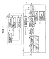
- FIG. 1 is a block diagram showing the general arrangement of an embodiment of'a pulse signal transmission system according to the present invention.
- a pulse signal a composed of ordinary binary signals of "1" and "0" and having a fixed period T is generated by an information signal source 1 and is converted into a two-level AMI signal b by a code converter 3.
- a detection signal a' is generated, and it operates a zero substitution imparter 4 so as to execute a code conversion different from one in the usual case.
- a clock multiplier 2 multiplies a clock (timing) signal t used for the original signal, and the multiplied signal is applied to the code converter 3 as well as the zero substitution imparter 4.
- the received signal b is amplified into a signal.of fixed amplitude by a pre-amplifier 5' which is subjected to a flat automatic gain control (AGC) 5, whereupon the amplified signal is turned into a duobinary shaped signal e by a duobinary shaping circuit 6'.
- AGC flat automatic gain control
- the duobinary shaping circuit is constructed so as to also have the function of a roll-off filter (a low-pass filter for removing a high frequency component).
- a decision circuit 7 compares the duobinary shaped signal with a threshold value, to individually deliver plus and minus pulses to a zero substitution remover 9.
- the zero substitution remover 9 removes a regenerated signal resulting from the zero substitution, and its output is partly applied to a code converter 12 and partly to an error detector 10.
- the detected result of a code error by the error detector is partly applied to the code converter 12 so as to (modify a decoded signal.
- Another part of the detected result is sometimes transmitted to a terminal station through a fault location signal generator 11 in order to charify an error position.
- the by the code converter 12 detected result is converted/into a 2-level AMI code, which is delivered to the next transmission line.
- a clock extractor 8 prepares, clock signals as timing signals synchronous with the transmitted signal, in such -a way that a resonator having a resonance frequency equal to a bit rate is excited by the duobinary signal e.
- the clock signals are applied to the decision circuit 7, the zero substitution remover 9 and the code converter 12 as such.
- the characterizing features of the present invention are principally concerned with the portions of the zero substitution imparter 4, decision circuit 7 and zero substitution remover 9. Since the other portions have hitherto been known, the detailed description thereof shall be omitted.
- Figure 2 is a waveform diagram for explaining the 2-level AMI code and the duobinary shaping.
- (a) indicates the original information signal which consists of the binary signals of "1” and “0” and which has the fixed period T (clock rate).
- (b) indicates the 2-level AMI signal into which the signal a has been converted.
- "1" of the original information has the polarity (level) kept identical during a time slot and changed at the boundary of time slots, while "0" of the original information has the polarity inverted every 1 ⁇ 2 T of a time slot.
- (d) indicates the duobinary shaped signal, which has a waveform similar to one resulting from the addition between the signal (b) and a signal (c) obtained by delaying the signal (b) by (for example, the addition wherein the level of "0" is assumed -0.5 and that of "1" +0.5).
- the duobinary shaped signal has pulses generated in the places of the and with alternate polarities, original information "1" similarly to the so-called bipolar code. Accordingly, when a signal obtained through the full-wave rectification of the signal (d) is used for exciting the resonator having the resonance frequency , the timing (clock) signal can be readily extracted. However, when "0's" have succeeded in the original information, no pulse appears in the duobinary shaped signal. In the prior-art pulse transmission system, therefore, a case occurs where the timing signal cannot be extracted.
- FIG. 3 is a waveform diagram for explaining the principle of the present invention.
- (a) indicates the original information signal, as to which the zero substitution is conducted when six "O's" have followed “1".
- a signal (b') does not conform with the normal 2-level AMI signal conversion rules. Polarities are not changed at the boundary of the second and third time slots T 2 , T 3 and the boundary of the sixth and seventh time slots T 6 , T 7 (with marks x attached). In each of the fourth and fifth time slots T 4 , T 5 (with marks O attached), the same polarity is held as in the case of "1" in spite of the original information being "0".
- the part in which the two-level AMI signal corresponding tc the succession of a certain number of "0's" is converted into the two-level signals not conforming with the normal rules in this manner, shall be called the "zero substitution”.
- pulses of widths T (including plus and minus pulses) at the mark x and at the mark o shall be respectively called the “pulses inphase with and antiphase to the original information.
- the ccnversion effected at the mark X shall be called the "violation".
- (d') indicates the duobinary shaped signal of the signal (b'). That is, it is obtained by adding the signal (b') and a signal with this signal (b') delayed by .
- the duobinary-shaped signal becomes a signal in a dull waveform and with a time delay ⁇ T as shown at (e), on account of transmission characteristics.
- This signal is sampled at timings (period T) shown at (f), compared with a threshold value, and waveshaped. Then, a waveform as shown at (g) is obtained.
- the duobinary shaped signal (e) produces pulses in the part where the original information "0's" succeed. Therefore, it can detect the levels of the input signal and can be used as the control signal of the AGC. Further, since the pulses having peak values develop at the sampling points t 4 and t 5 , the timing signal is easily extracted. That is, when the.resonator is excited by the pulses having the peaks at t4 and t 5 , it is effectively excited.
- the pulses at the positions of the violation become antiphase and act to cancel the timing signal because of the peak values lying midway between the sampling points. Since, however, the inphase pulses arising at t 4 and t 5 are adjacent to each other, they have the effect of emphasizing the timing component, so that the timing signal is not lost in spite of equal numbers of the inphase and antiphase pulses.
- the positions of the regenerated waveform (g) at the points of time t 2 and t 3 are undefined as to whether they are "0" or "+1".
- the positions of the regenerated waveform at the points of time t 6 and t 7 are undefined as to whether they are "0" or "-1". (Such undefined parts are indicated by dotted lines.)
- the zero substitution part is decided and removed by utilizing the properties of the regenerated waveform (g) and the two-level AMI signal.
- the undefined pulses to become "0" or "+1” are denoted by ⁇ + and the undefined pulses to become "0" or "-1” are denoted by ⁇ - , the signal of the succession of the six "0's" becomes " ⁇ + ,
- the invention utilizes the property of the duobinary shaped signal of the two-level AMI signal, that is, the property that "+1 " and "-1" arise alternately. In the case of Figure 3, "1" exists before the succession of "0's".
- the signal part can therefore be decided as the regenerated signal based on the zero substitution, because ⁇ + cannot become -1 in "1, ⁇ + , ⁇ + , 1, -1, ⁇ - , ⁇ - ".
- the part " ⁇ + , ⁇ + , +1, -1, ⁇ - , ⁇ - " is converted into "0, 0, 0, 0, 0, 0"
- the removal of the zero substitution is realized.
- the present invention is not restricted to the example but is also applicable to cases of executing the zero substitution of a succession of seven or more "O's" as indicated in an embodiment to be described later. In those cases, the zero substitution part can be decided without considering the regenerated signal of the preceding -original information "1" as will be described later.
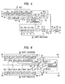
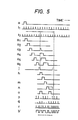
- Figure 4 is a diagram showings the arrangement of an embodiment of the transmitting part in Figure 1, while Figure 5 is a time chart for explaining the operation of the embodiment.
- the zero substitution in the present embodiment for the succession of "0's" is executed in conformity with the rules illustrated in Figure 3.
- the original information signal a is assumed to be a pulse signal wherein the first value is "1" after which "0's" succeed.
- the signal a is applied to the input terminal 14 of a shift register 13 in which flip-flop circuits are connected in six stages (13-1 to 13-6) and which is operated by a clock signal t 2 having a period T. With the lapse of time, the output waveforms of the respective stages become as shown at a 1 - a 6 in Figure 5.
- the succession of six "0's" in the original information can be detected by obtaining the logical sum (OR) of the outputs of the respective stages of the shift register 13.
- the outputs of OR gates 15 and 16 are applied to a NOR gate 17, whereby the output j of the NOR gate 17 becomes "1" when the six "0's" have succeeded in the original information.
- the pulse of a clock signal t (having a period T and shifting by 1 which is with respect to the clock signal t 2 ) applied to an input terminal 18 has arrived, the third and fourth stages of flip-flops 13-3 and 13-4 of the shift register 13 are set at "1" through an AND gate 19.
- the operation is intended to generate two inphase pulses (of "+1 " and "-1") at this point of time (refer to Figure 3).
- the clock t l of an AND gate 20 is inhibited by the waveform a 6 , to obtain a train of pulses q (thus, inphase pulses are obtained as stated below).
- a train of pulses p is obtained (thus, antiphase pulses can be obtained).
- the trains of pulses p and q are combined by an OR gate 24 into a train of pulses r, which is applied to a T-type flip-flop 25 as a trigger signal.
- the zero-substituted two-level AMI signal b' shown in Figure 3 is provided from the output terminal 26 of the T-type flip-flop 25.
- a pulse expander 27 in Figure 4 expands the output of the fourth stage of the shift register 21 as indicated by a dotted line in the waveform n of Figure 5. This serves for securing the last point of time of the 6-bit violation in order to prevent the next pulse j for zero succession detection (a part indicated by a dotted line) from arising earlier.
- Figure 6 is a circuit diagram showing the arrangement of an embodiment of the zero substitution remover 9 in the receiving part. It is a circuit corresponding to a case where the two-level AMI signal s produced by the embodiment of Figure 4 has been received as an input signal.
- the duobinary shaped signal (e) is a pulse train of the three levels of "+1", the signal e "0" and "-1".
- a pulse train hereinbelow, called the "P pulse train” wherein only the pulses of "+1” in the signal e are denoted as “1” and the others (of "0” and “-1") as "0”
- a pulse train hereinbelow, called the “N pulse train” wherein only the pulses of "-1” in the signal e are denoted as "1” and the others (of "0” and “+1") as "0”
- the P pulse train and the N pulse train are respectively applied to the input terminals 29 and 30 of shift registers 27 and 28.
- the regenerated pulse train of the zero substitution part becomes " ⁇ + , ⁇ + , 1, -1, ⁇ - , ⁇ - " as stated before.
- ⁇ + is either "+1” or "0”
- ⁇ - is either "-1" or "0”. Therefore, regarding the N pulse train, the first, second and third stages of the shift register 29 become “0” necessarily, and the fourth stage becomes “1” necessarily.
- the third stage becomes “1” necessarily, and the fourth, fifth and sixth stages become “0" necessarily.
- the pulse train " ⁇ + , ⁇ +, 1, -1, ⁇ - , ⁇ -" can accordingly be decided to be the signal based on the zero substitution, by logic processing as stated below.
- a NOR gate 31 accordingly provides "1" with the above logical sum inverted, in correspondence with the violation part.
- This signal is used as an antiphase pulse detection signal, and "1" indicates the possibility of the occurrence of ⁇ + and ⁇ - .
- the logical sum (AND) between the output of the third stage of flip-flop circuit 27-3 of the shift register 27 and that of the fourth stage of flip-flop circuit 28-4 of the shift register 28 is found. When it is “1”, there is the possibility that the inphase pulses "1” and "-1" have arisen in the violation. This signal is used as an inphase pulse detection signal.
- the inphase pulse detection signal and the antiphase pulse detection signal are "1"
- the possibility of the occurrence of the violation is high, but the original information signal might include the same pattern.
- the output of the seventh stage 27-7 of the shift register 27 may be checked.
- the zero substitution detection pulse may be stored in a shift register 35 (constructed of six stages) in advance, and it may be checked. Accordingly, the logical sum between the outputs of the shift register 35 and the seventh stage 27-7 of the shift register 27 is obtained by means of an OR gate 33.
- the output of the OR gate 33 shall be called the "preceding state acknowledgement signal".
- FIGS 7 and 8 show circuit diagrams of other embodiments of the code converter in the transmitting part and the zero substitution remover in the receiving part in another embodiment of the code transmission system according to the present invention, respectively.
- the arrangement and operation of the embodiment in Figure 7 will be described with reference to a time chart in Figure 10.
- the original information signal a (the same as that shown at a in Figure 9) is applied to the input end 41 of a shift register 45, which has nine stages of flip-flops (45-1 to 45-9) connected in series, in synchronism with a timing signal t 2 of a period T. With the lapse of time, the outputs of the respective stages of the shift register 45 become as shown at a l - a 8 in Figure 10.
- OR gates 47, 48 and a NOR gate 49 are used for detecting the succession of eight "0's" which are the outputs of the respective stages (l).
- Figure 8 shows the arrangement of one embodiment of the circuit for detecting and removing the zero substitution from the two-level AMI signal which has been obtained by the embodiment of Figure 7 and which contains the zero substitution.
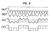
- the decision circuit 7 in Figure 1 converts the signal of the three levels of "+1", "0" and "-1", which is the duobinary shaped signal (e) or (f) in Figure 9, into a train of pulses (P pulse train) wherein the pulse of "+1 " is made “1" and the others ("0” and “-1") are made “0", and a train of pulses (N pulse train) wherein only the pulse of "-1" is made “1” and the others ("0” and “ + 1") are made “0".
- P pulse train train of pulses
- N pulse train wherein only the pulse of "-1" is made "1" and the others
- an AND gate 62 which receives the outputs of the first and fourth stages 60-1, 60-4 of a shift register 60 and the inverted signals of the outputs of the second and third stages 61-2, 61-3 of a shift register 61
- an AND gate 6L which receives the inverted signals of the outputs of the second and third stages 60-2, 60-3 cf the shift register 60 and the outputs of the first and fourth stages 61-1, 61-4 of the shift register 61.
- the outputs of the respective AND gates are applied to an OR gate 63. Then, only when the zero substitution has arisen, a pulse is provided from an output terminal 65.
- the execution of zero substitution is permitted in case of performing the duobinary shaping of a two-level AMI signal. Even when "0's" succeed in original information, the extraction of a timing signal and the AGC are facilitated, and besides, a zero substitution part in the case of executing the zero substitution including violation can be properly detected.
Landscapes
- Physics & Mathematics (AREA)
- Spectroscopy & Molecular Physics (AREA)
- Engineering & Computer Science (AREA)
- Computer Networks & Wireless Communication (AREA)
- Signal Processing (AREA)
- Dc Digital Transmission (AREA)
- Optical Communication System (AREA)
Applications Claiming Priority (2)
| Application Number | Priority Date | Filing Date | Title |
|---|---|---|---|
| JP57042763A JPS58161554A (ja) | 1982-03-19 | 1982-03-19 | パルス信号伝送システム |
| JP42763/82 | 1982-03-19 |
Publications (2)
| Publication Number | Publication Date |
|---|---|
| EP0089467A1 true EP0089467A1 (de) | 1983-09-28 |
| EP0089467B1 EP0089467B1 (de) | 1986-04-23 |
Family
ID=12645012
Family Applications (1)
| Application Number | Title | Priority Date | Filing Date |
|---|---|---|---|
| EP83100759A Expired EP0089467B1 (de) | 1982-03-19 | 1983-01-27 | Verfahren und System zur Impulssignalübertragung |
Country Status (5)
| Country | Link |
|---|---|
| US (1) | US4503546A (de) |
| EP (1) | EP0089467B1 (de) |
| JP (1) | JPS58161554A (de) |
| CA (1) | CA1192313A (de) |
| DE (1) | DE3363122D1 (de) |
Families Citing this family (11)
| Publication number | Priority date | Publication date | Assignee | Title |
|---|---|---|---|---|
| US4785466A (en) * | 1987-06-18 | 1988-11-15 | Siemens Transmission Systems, Inc. | Encoder/decoder circuit for B8ZS and B6ZS applications |
| US4885582A (en) * | 1987-09-28 | 1989-12-05 | The Grass Valley Group, Inc. | "Simple code" encoder/decoder |
| US4860009A (en) * | 1988-02-12 | 1989-08-22 | Paradyne Corporation | Bidirectional multiframe converter for data communications systems |
| JPH0710047B2 (ja) * | 1988-09-14 | 1995-02-01 | 富士通株式会社 | 零連誤り検出回路 |
| JPH02312329A (ja) * | 1989-05-27 | 1990-12-27 | Fujitsu Ltd | 信号伝送方式 |
| JPH04154229A (ja) * | 1990-10-18 | 1992-05-27 | Fujitsu Ltd | 非同期3次群信号による対局警報通信方式 |
| US5130608A (en) * | 1990-11-02 | 1992-07-14 | Nicholas Zahardis | Electrical module and method for reducing power consumption of an incandescent light bulb |
| FR2719175B1 (fr) * | 1994-04-20 | 1996-05-31 | Cit Alcatel | Procédé de transmission optique présentant une sensibilité réduite à la dispersion, et système de transmission pour la mise en Óoeuvre de ce procédé. |
| US5631928A (en) * | 1995-05-26 | 1997-05-20 | Nec America, Inc. | Enhanced B3ZS decoder and method for identifying true zero-substitutions |
| KR20020046118A (ko) * | 2000-12-12 | 2002-06-20 | 정용주 | 단극성 최소대역폭 신호 성형 방법 및 전송장치 |
| US7835100B2 (en) * | 2007-11-01 | 2010-11-16 | Safonov Vladimir L | Logic operations on a hard disk drive |
Citations (1)
| Publication number | Priority date | Publication date | Assignee | Title |
|---|---|---|---|---|
| EP0013990A1 (de) * | 1979-01-30 | 1980-08-06 | COMPAGNIE LYONNAISE DE TRANSMISSIONS OPTIQUES Société anonyme dite: | Verfahren zur serienförmigen Übertragung binärer Informationen und Vorrichtungen zur Durchführung des Verfahrens |
Family Cites Families (5)
| Publication number | Priority date | Publication date | Assignee | Title |
|---|---|---|---|---|
| US3665103A (en) * | 1969-12-16 | 1972-05-23 | Ibm | Synchronous frequency shift data transmission system in which opposite binary characterizations are transmitted as half cycles of a first carrier signal and as full cycles of a second carrier signal |
| GB1489177A (en) * | 1973-10-16 | 1977-10-19 | Gen Electric Co Ltd | Digital data signalling systems and apparatus therefor |
| GB1512700A (en) * | 1975-10-23 | 1978-06-01 | Standard Telephones Cables Ltd | Data transmission |
| GB1566223A (en) * | 1978-01-17 | 1980-04-30 | Standard Telephones Cables Ltd | Digital duplex transmission system |
| US4267595A (en) * | 1980-02-04 | 1981-05-12 | International Telephone And Telegraph Corporation | AMI Decoder apparatus |
-
1982
- 1982-03-19 JP JP57042763A patent/JPS58161554A/ja active Granted
-
1983
- 1983-01-27 EP EP83100759A patent/EP0089467B1/de not_active Expired
- 1983-01-27 DE DE8383100759T patent/DE3363122D1/de not_active Expired
- 1983-02-09 CA CA000421247A patent/CA1192313A/en not_active Expired
- 1983-03-01 US US06/471,128 patent/US4503546A/en not_active Expired - Lifetime
Patent Citations (1)
| Publication number | Priority date | Publication date | Assignee | Title |
|---|---|---|---|---|
| EP0013990A1 (de) * | 1979-01-30 | 1980-08-06 | COMPAGNIE LYONNAISE DE TRANSMISSIONS OPTIQUES Société anonyme dite: | Verfahren zur serienförmigen Übertragung binärer Informationen und Vorrichtungen zur Durchführung des Verfahrens |
Non-Patent Citations (3)
| Title |
|---|
| INTERNATIONAL CONFERENCE ON COMMUNICATIONS, June 10-14, 1979, BOSTON, MA, CONFERENCE RECORD, vol. 4,pages 53.2.1-53.2.5, IEEE cat. no. 79CH1435-7 CSCB, New York, US * |
| INTERNATIONAL CONFERENCE ON COMMUNICATIONS, June 16-18, 1975, San francisco, conference record vol. II, IEEE cat. no. 75 CH0 971-2 CSCB, pages 32-20 to 32-24, New York, US * |
| NACHRICHTENTECHNIK ELEKTRONIK, vol. 31, no. 9, 1981, pages 356-362, East Berlin, DD * |
Also Published As
| Publication number | Publication date |
|---|---|
| EP0089467B1 (de) | 1986-04-23 |
| US4503546A (en) | 1985-03-05 |
| JPS58161554A (ja) | 1983-09-26 |
| JPH059975B2 (de) | 1993-02-08 |
| CA1192313A (en) | 1985-08-20 |
| DE3363122D1 (en) | 1986-05-28 |
Similar Documents
| Publication | Publication Date | Title |
|---|---|---|
| EP0610204B1 (de) | Leitungskode, mit blockinvertierung, für schnelle verbindungen | |
| EP0118763B1 (de) | Verfahren zur Fehlerortung in einer digitalen Übertragungsleitung | |
| US4964138A (en) | Differential correlator for spread spectrum communication system | |
| US5623518A (en) | Method and circuit arrangement for transmitting binary data trains | |
| EP0089467A1 (de) | Verfahren und System zur Impulssignalübertragung | |
| FI89436B (fi) | Synkronisationsregenerering i telekommunikationssystem | |
| US5898734A (en) | Symbol determining method and apparatus | |
| EP0090728B1 (de) | Verfahren zur gemeinsamen Übertragung eines Signals im HDBN-Kode und eines binären Hilfssignals, Kodierer und Dekodierer nach diesem Verfahren und System zur Fernüberwachung von Zwischenverstärkern einer Digitalverbindung mit Hilfe solcher Hilfssignale | |
| US4276650A (en) | Method of synchronizing a quadphase receiver and clock synchronization device for carrying out the method | |
| EP0304081A2 (de) | Digitales Übertragungsverfahren mit Pseudo-Mehrstufen und bipolaren Kodierungstechniken | |
| EP0568804A2 (de) | Übertragungssteuerungsvorrichtung | |
| EP0174182B1 (de) | Informationsübertragungssystem in einem für Kollisionserkennung geeigneten lokalen Netz | |
| KR100337020B1 (ko) | 동일채널에서동작하는신호들을분리하기위한방법및장치 | |
| EP0568314A2 (de) | Dezentrales Datenverarbeitungssternnetz und dazugehörige Konzentrator und Endgeräte | |
| US4675545A (en) | Wave shaping apparatus for eliminating pulse width distortion | |
| US4438520A (en) | System for regenerating a data word on a communications ring | |
| US7260151B2 (en) | Dual phase pulse modulation system | |
| JPS6022854A (ja) | デイジタル信号変復調方式 | |
| JP2000013451A (ja) | 光デ−タの受信装置 | |
| JPH0528547B2 (de) | ||
| RU1775856C (ru) | Способ декодировани бипол рных кодов и устройство дл его осуществлени | |
| EP0633669B1 (de) | Verfahren und Vorrichtung zur Erfassung von gesendeten Daten in einer elektrischen Energieverteilungsanlage | |
| JP3998637B2 (ja) | 雑音排除情報伝送方法 | |
| JPS60176350A (ja) | 符号変換方法 | |
| JPH05226938A (ja) | 周波数変調符号化データ復調方法及び復調装置 |
Legal Events
| Date | Code | Title | Description |
|---|---|---|---|
| PUAI | Public reference made under article 153(3) epc to a published international application that has entered the european phase |
Free format text: ORIGINAL CODE: 0009012 |
|
| AK | Designated contracting states |
Designated state(s): DE FR GB IT NL SE |
|
| 17P | Request for examination filed |
Effective date: 19830930 |
|
| GRAA | (expected) grant |
Free format text: ORIGINAL CODE: 0009210 |
|
| AK | Designated contracting states |
Kind code of ref document: B1 Designated state(s): DE FR GB IT NL SE |
|
| REF | Corresponds to: |
Ref document number: 3363122 Country of ref document: DE Date of ref document: 19860528 |
|
| ITF | It: translation for a ep patent filed | ||
| ET | Fr: translation filed | ||
| PLBE | No opposition filed within time limit |
Free format text: ORIGINAL CODE: 0009261 |
|
| STAA | Information on the status of an ep patent application or granted ep patent |
Free format text: STATUS: NO OPPOSITION FILED WITHIN TIME LIMIT |
|
| 26N | No opposition filed | ||
| ITTA | It: last paid annual fee | ||
| EAL | Se: european patent in force in sweden |
Ref document number: 83100759.6 |
|
| PGFP | Annual fee paid to national office [announced via postgrant information from national office to epo] |
Ref country code: SE Payment date: 19960118 Year of fee payment: 14 |
|
| PG25 | Lapsed in a contracting state [announced via postgrant information from national office to epo] |
Ref country code: SE Effective date: 19970128 |
|
| EUG | Se: european patent has lapsed |
Ref document number: 83100759.6 |
|
| REG | Reference to a national code |
Ref country code: GB Ref legal event code: IF02 |
|
| PGFP | Annual fee paid to national office [announced via postgrant information from national office to epo] |
Ref country code: GB Payment date: 20020107 Year of fee payment: 20 |
|
| PGFP | Annual fee paid to national office [announced via postgrant information from national office to epo] |
Ref country code: FR Payment date: 20020118 Year of fee payment: 20 |
|
| PGFP | Annual fee paid to national office [announced via postgrant information from national office to epo] |
Ref country code: NL Payment date: 20020131 Year of fee payment: 20 |
|
| PGFP | Annual fee paid to national office [announced via postgrant information from national office to epo] |
Ref country code: DE Payment date: 20020328 Year of fee payment: 20 |
|
| PG25 | Lapsed in a contracting state [announced via postgrant information from national office to epo] |
Ref country code: GB Free format text: LAPSE BECAUSE OF EXPIRATION OF PROTECTION Effective date: 20030126 |
|
| PG25 | Lapsed in a contracting state [announced via postgrant information from national office to epo] |
Ref country code: NL Free format text: LAPSE BECAUSE OF EXPIRATION OF PROTECTION Effective date: 20030127 |
|
| REG | Reference to a national code |
Ref country code: GB Ref legal event code: PE20 Effective date: 20030126 |
|
| NLV7 | Nl: ceased due to reaching the maximum lifetime of a patent |
Effective date: 20030127 |