EP0090111A2 - Procédé pour la fabrication d'un dispositif semi-conducteur comportant des régions d'isolation diélectriques - Google Patents
Procédé pour la fabrication d'un dispositif semi-conducteur comportant des régions d'isolation diélectriques Download PDFInfo
- Publication number
- EP0090111A2 EP0090111A2 EP82305018A EP82305018A EP0090111A2 EP 0090111 A2 EP0090111 A2 EP 0090111A2 EP 82305018 A EP82305018 A EP 82305018A EP 82305018 A EP82305018 A EP 82305018A EP 0090111 A2 EP0090111 A2 EP 0090111A2
- Authority
- EP
- European Patent Office
- Prior art keywords
- semiconductor substrate
- mask member
- groove
- mask
- impurity
- Prior art date
- Legal status (The legal status is an assumption and is not a legal conclusion. Google has not performed a legal analysis and makes no representation as to the accuracy of the status listed.)
- Granted
Links
Images

Classifications
-
- H—ELECTRICITY
- H10—SEMICONDUCTOR DEVICES; ELECTRIC SOLID-STATE DEVICES NOT OTHERWISE PROVIDED FOR
- H10P—GENERIC PROCESSES OR APPARATUS FOR THE MANUFACTURE OR TREATMENT OF DEVICES COVERED BY CLASS H10
- H10P30/00—Ion implantation into wafers, substrates or parts of devices
- H10P30/20—Ion implantation into wafers, substrates or parts of devices into semiconductor materials, e.g. for doping
- H10P30/222—Ion implantation into wafers, substrates or parts of devices into semiconductor materials, e.g. for doping characterised by the angle between the ion beam and the crystal planes or the main crystal surface
-
- H—ELECTRICITY
- H10—SEMICONDUCTOR DEVICES; ELECTRIC SOLID-STATE DEVICES NOT OTHERWISE PROVIDED FOR
- H10D—INORGANIC ELECTRIC SEMICONDUCTOR DEVICES
- H10D30/00—Field-effect transistors [FET]
- H10D30/60—Insulated-gate field-effect transistors [IGFET]
-
- H—ELECTRICITY
- H10—SEMICONDUCTOR DEVICES; ELECTRIC SOLID-STATE DEVICES NOT OTHERWISE PROVIDED FOR
- H10D—INORGANIC ELECTRIC SEMICONDUCTOR DEVICES
- H10D62/00—Semiconductor bodies, or regions thereof, of devices having potential barriers
- H10D62/10—Shapes, relative sizes or dispositions of the regions of the semiconductor bodies; Shapes of the semiconductor bodies
- H10D62/102—Constructional design considerations for preventing surface leakage or controlling electric field concentration
- H10D62/112—Constructional design considerations for preventing surface leakage or controlling electric field concentration for preventing surface leakage due to surface inversion layers, e.g. by using channel stoppers
-
- H—ELECTRICITY
- H10—SEMICONDUCTOR DEVICES; ELECTRIC SOLID-STATE DEVICES NOT OTHERWISE PROVIDED FOR
- H10P—GENERIC PROCESSES OR APPARATUS FOR THE MANUFACTURE OR TREATMENT OF DEVICES COVERED BY CLASS H10
- H10P30/00—Ion implantation into wafers, substrates or parts of devices
- H10P30/20—Ion implantation into wafers, substrates or parts of devices into semiconductor materials, e.g. for doping
- H10P30/22—Ion implantation into wafers, substrates or parts of devices into semiconductor materials, e.g. for doping using masks
- H10P30/221—Ion implantation into wafers, substrates or parts of devices into semiconductor materials, e.g. for doping using masks characterised by the angle between the ion beam and the mask
-
- H—ELECTRICITY
- H10—SEMICONDUCTOR DEVICES; ELECTRIC SOLID-STATE DEVICES NOT OTHERWISE PROVIDED FOR
- H10W—GENERIC PACKAGES, INTERCONNECTIONS, CONNECTORS OR OTHER CONSTRUCTIONAL DETAILS OF DEVICES COVERED BY CLASS H10
- H10W10/00—Isolation regions in semiconductor bodies between components of integrated devices
- H10W10/01—Manufacture or treatment
- H10W10/011—Manufacture or treatment of isolation regions comprising dielectric materials
- H10W10/014—Manufacture or treatment of isolation regions comprising dielectric materials using trench refilling with dielectric materials, e.g. shallow trench isolations
- H10W10/0148—Manufacture or treatment of isolation regions comprising dielectric materials using trench refilling with dielectric materials, e.g. shallow trench isolations comprising introducing impurities in side walls or bottom walls of trenches, e.g. for forming channel stoppers
-
- H—ELECTRICITY
- H10—SEMICONDUCTOR DEVICES; ELECTRIC SOLID-STATE DEVICES NOT OTHERWISE PROVIDED FOR
- H10W—GENERIC PACKAGES, INTERCONNECTIONS, CONNECTORS OR OTHER CONSTRUCTIONAL DETAILS OF DEVICES COVERED BY CLASS H10
- H10W10/00—Isolation regions in semiconductor bodies between components of integrated devices
- H10W10/10—Isolation regions comprising dielectric materials
- H10W10/17—Isolation regions comprising dielectric materials formed using trench refilling with dielectric materials, e.g. shallow trench isolations
-
- Y—GENERAL TAGGING OF NEW TECHNOLOGICAL DEVELOPMENTS; GENERAL TAGGING OF CROSS-SECTIONAL TECHNOLOGIES SPANNING OVER SEVERAL SECTIONS OF THE IPC; TECHNICAL SUBJECTS COVERED BY FORMER USPC CROSS-REFERENCE ART COLLECTIONS [XRACs] AND DIGESTS
- Y10—TECHNICAL SUBJECTS COVERED BY FORMER USPC
- Y10S—TECHNICAL SUBJECTS COVERED BY FORMER USPC CROSS-REFERENCE ART COLLECTIONS [XRACs] AND DIGESTS
- Y10S148/00—Metal treatment
- Y10S148/085—Isolated-integrated
Definitions
- the present invention relates to a method for manufacturing a semiconductor device and, more particularly, to an improvement in an element isolation technique in the manufacture of integrated circuits (ICs).
- ICs integrated circuits
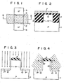
- Fig. 1 is a plan view of a MOSFET
- Fig. 2 is a sectional view thereof taken along the line II - II of Fig. 1.
- a semiconductor substrate 1 comprises p-type silicon.
- An island element region which is isolated by a thick silicon oxide layer 2 is formed on the p-type semiconductor substrate 1.
- N-type source and drain regions 3 and 4 which are electrically insulated from each other are formed in the element region.
- a p-type channel region 5 is formed between the n-type source and drain regions 3 and 4.
- a gate electrode 7 of polycrystalline silicon is deposited on the channel region 5 through a gate oxide layer 6. It is noted that the element region of the p-type semiconductor substrate 1 formed by etching to extend above the level of the other surface portions, and the silicon oxide layer 2 is formed to surround the element region.
- the amount of the impurity must be precisely controlled.
- ion-implantation is the best method to increase the concentration of the impurity.
- ion-implantation has directivity.
- the p-type semiconductor substrate 1 is selectively etched to expose a portion thereof, using a mask member 9 which comprises a resist material and which has a predetermined shape. Thereafter, a p-type impurity such as boron is ion-implanted perpendicularly to one major surface of the p-type semiconductor substrate 1 to form p -type channel-cut regions 10 in the etched bottom portions.
- channel-cut regions are not formed on the side surfaces 8 of the element region.
- the impurity In order to form p +- type channel-cut regions on the side surfaces 8 of the element region, as shown in Fig. 4, the impurity must be ion-implanted obliquely with respect to one major surface of the semiconductor substrate 1.
- channel-cut regions 10' are formed respectively on the side surfaces 8 of the element region.
- the side surfaces of the element region which extend above other surface portions of the semiconductor substrate are oriented in various directions in an integrated circuit. Therefore, it is not desirable to ion implant the impurity obliquely in mass production.
- a method for manufacturing a semiconductor device comprising the steps of: forming a first mask member which has an opening to expose a desired portion of one major surface of a semiconductor substrate; doping an impurity which has the same conductivity type as a conductivity type of said semiconductor substrate through said opening of said first mask member to form an impurity region of a high concentration in a surface layer of said semiconductor substrate; forming a second mask member on a side surface of said opening of said first mask member while said first mask member is left as it is; forming a groove by selectively etching said semiconductor substrate using said first and second mask members, and at the same time leaving an impurity region of the high concentration at least on a side surface of said groove; and burying an insulating isolation material in said groove.
- a method for manufacturing a semiconductor device comprising the steps of: forming a first mask member which has an opening to expose a desired portion of one major surface of a semiconductor substrate; forming a second mask member on a side surface of said opening; forming a groove by selectively etching said semiconductor substrate using said first and second mask members; removing said second mask member; doping an impurity which has the same conductivity type as a conductivity type of said semiconductor substrate through said opening of said first mask member to form an impurity region of a high concentration at least on a side surface of said groove; and burying an insulating isolation material in said groove.
- a first mask member which has an opening of a desired shape is formed on a semiconductor substrate.
- the first mask member may comprise a metal pattern such as an aluminum pattern, or a pattern such as a silicon oxide pattern or a silicon nitride pattern.
- a thin silicon oxide film may be interposed between the first mask member and the semiconductor substrate.
- An impurity which has the same conductivity type as that of the semiconductor substrate is ion-implanted or thermally diffused in the semiconductor substrate through the opening of the first mask member to form an impurity region of a high concentration.
- a thin film as a second prospective mask member is deposited on the first mask member to cover the entire surface to a thickness greater than half of the width of the opening of the first mask member.
- the thin film must be made of a material which is etched using the first mask member as a mask.
- the first mask member comprises aluminum
- the thin film may comprise a silicon oxide or silicon nitride film.
- the first mask comprises silicon nitride
- the thin film may comprise an aluminum or silicon oxide film.
- anisotropic etching such as reactive ion etching (RIE) is performed to etch the thin film perpendicularly to one major surface of the semiconductor substrate along the entire thickness of the thin film.
- RIE reactive ion etching
- the impurity region under the semiconductor substrate, or the impurity region and the portion of the semiconductor substrate thereunder are selectively etched by anisotropic etching such as the RIE method to form a groove and to leave the impurity portion on the side surface of the groove.
- the side surface of the groove becomes vertical or substantially vertical.
- an impurity which has the same conductivity type as that of the semiconductor substrate is ion-implanted in the bottom of the groove using the first and second mask members and is doped to form an impurity region of a high concentration.
- Channel-cut regions are formed on the side surface of the convex-shaped element region and the etched surface (bottom surface of the groove), in the same structure described with reference to Fig. 4.
- the element isolation region is formed to electrically isolate the island semiconductor region (element formation region) surrounded by the groove.
- the groove may be formed by the following methods:
- an insulating film or a film which comprises a material to be oxidized may be deposited.
- the insulating film or a film which comprises a material to be oxidized may be deposited.
- the film is etched to expose the first mask member. The isolating material which extends above the surface of the semiconductor substrate is formed to cover the side surface of the groove and the side surface of the residual impurity portion.
- the junctions between the source region and the semiconductor substrate and between the drain region and the semiconductor substrate may not be exposed through the surface of the semiconductor substrate. Especially, the junctions may not be short-circuited when source and drain electrodes are deposited.
- the present invention provides a method for manufacturing a semiconductor device, wherein an impurity which has the same conductivity type as that of the semiconductor substrate is doped in the semiconductor substrate through the opening of the first mask member to form an impurity region of a high concentration, a second mask member is formed on the side surface of the opening of the first mask member, and a channel-cut region is easily formed with excellent controllability on the side surface of the element region extending above the surface of the semiconductor substrate by selectively etching the semiconductor substrate using the first and second mask members.
- a first mask member which has an opening with a desired shape is formed on a semiconductor substrate.
- anisotropic etching such as the RIE method is performed to vertically etch the thin film with respect to the major surface of the semiconductor substrate along the entire thickness of the thin film.
- the thin film portion is left on the side surface of the opening of the first mask member.
- the second mask member is formed.
- the semiconductor substrate is selectively etched to form a groove using the first and second mask members.
- an impurity which has the same conductivity type as that of the semiconductor substrate is ion-implanted and is diffused to form impurity regions of a high concentration on the side surface and the bottom of the groove.
- an isolation member is formed in the side surfaces and the bottom of the groove which has the channel-cut regions therein in accordance with one of methods (1) to (3) described above.
- the island semiconductor region surrounded by the groove is electrically isolated by the element isolation region.
- the second embodiment is the same as the first embodiment except that the order of the step of forming the groove and the step of forming an impurity region of a high concentration on the side surface of the groove is reversed.
- the second embodiment of the present invention provides a method for manufacturing a semiconductor device wherein a channel-cut region can be readily formed with excellent controllability on the side surface of the element region which extends above the surface of the semiconductor substrate.
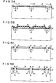
- a silicon oxide film 12 0 of about 1,000 A thickness was grown by thermal oxidation on the major surface of a p-type silicon substrate 11 whose impurity concentration was 3 x 10 13 cm-3.
- An aluminum film was then deposited by vacuum deposition to cover the entire surface to a 0 thickness of about 5,000 A.
- Lattice-shaped openings 14 were formed by patterning the aluminum film except for the portions of prospective element isolation regions.
- a p-type impurity (boron) was then ion-implanted at a dose of 1 x 10 13 cm -2 and at an acceleration concentration of 200 KeV in the silicon substrate 11 through the silicon oxide film 12 using a first mask pattern 13 which comprised the aluminum.
- the impurity was activated to form p +- type impurity regions 15.
- the depth of each of the p +- type impurity regions 15 was 0.3 ⁇ m.
- the impurity was diffused in an atmosphere of N 2 gas for about 20 minutes and each of the p +- type impurity regions 15 had a final depth of 0.5 ⁇ m.
- a thin CVD-Si0 2 film 16 was deposited to cover the entire surface to a thickness (e.g., 3 ⁇ m) less than half of the width of the opening 14.
- anisotropic etching such as RIE was performed to etch the CVD-Si0 2 film 16 vertically with respect to the major surface of the silicon substrate 11, as shown in Fig. 5C.
- the silicon oxide film 12 was subsequently etched by the RIE method.
- power for the RIE method was set to the general high frequency power, and CF 4 gas (Freon gas) was used as the etchant.
- second mask patterns 17 which comprised thin SiO 2 films were left on the side surfaces of the openings 14 of the first mask patterns 13.
- the exposed portions of the silicon substrate 11 were etched by the RIE method using the first and second mask patterns 13 and 17 to form grooves 18 each of which had vertical or substantially vertical side surfaces and had a depth of 0.6 ⁇ m.
- a gas mixture of Cl 2 gas and H 2 gas was used as an etchant.
- P + -type channel cut regions 19 were respectively left at the side surfaces of the groove 18. Since the depth of the groove 18 was 0.6 ⁇ m, the bottom thereof reached the silicon substrate 11 beyond the bottom of the p + -type channel-cut region 15. As shown in Fig.
- boron was ion-implanted in the silicon substrate 11 at a dose of about 1 x 10 13 cm -2 and at an acceleration voltage of 40 KeV using the second mask patterns 17 and the first mask patterns 13. Boron was then diffused to form p +- type channel stoppers 20 in the bottoms of the grooves 18.
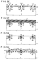
- an island region of the silicon substrate 11 which was isolated by the element isolation region 23 was thermally oxidized to grow an oxide film.
- an arsenic-doped polycrystalline silicon film was deposited on the oxide film.
- the arsenic-doped polycrystalline silicon film was then patterned to form a plurality of gate electrodes 24.
- the oxide film was then selectively etched using the gate electrodes 24 as masks, so that gate oxide films 25 were formed.
- An n-type impurity such as arsenic was ion-implanted in the silicon substrate using the gate electrodes 24 and the element isolation regions 23 as masks.
- Arsenic was then diffused to a depth of about 0.3 ⁇ m to form n +- type impurity regions 26 which functioned as the source and drain regions.
- n +- type impurity regions 26 which functioned as the source and drain regions.
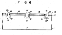
- the p +- type channel-cut regions 19 can be formed on the side surfaces of grooves 18 to have a thickness corresponding to the width of the second mask patterns 17. Therefore, unlike the conventional ion-implantation method, the impurity need not be obliquely doped. As a result, the channel-cut regions 19 are formed on the side surfaces of the grooves 18 which respectively constitute the element isolation regions. A parasitic channel which tends to be formed between the n +- type impurity regions 26 as the source and drain regions is prevented. Further, by arbitrarily changing the thickness of the residual CVD-Si0 2 patterns, a channel-cut region which has an arbitrary width can be formed on the side surface of the groove 18.
- p +- type channel stoppers 20 are formed in the bottoms of the grooves 18, a channel may not be formed under the groove 18 in the silicon substrate 11.
- the groove 18 when the groove 18 is formed using the second mask patterns 17, its bottom reaches the silicon substrate 11 beyond the bottom of the p -type region 15.
- the depth of the groove when the depth of the groove is set to be about 0.4 ⁇ m, which is one micron smaller than the depth (0.5 ⁇ m) of the p +- type region 15, a p +- type region 27 which functions both as the p +- type region (channel-cut region) 19 and the channel stopper 20 may be formed.
- the step of forming the channel stopper 20 can be omitted.
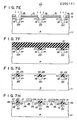
- first mask patterns 13 which respectively comprised aluminum films which had lattice-shaped openings 14 were formed on a p-type silicon substrate 11 through an oxide film 12.
- a thin CVD-Si0 2 film 16 was deposited to cover the entire surface including the area of the openings 14.
- the thin CVD-SiO 2 film 16 was etched by the RIE method along its entire thickness.
- second mask patterns 17 which respectively comprised thin CVD-SiO 2 films were formed on the side surfaces of the openings 14 of the first mask patterns 13.
- an Si0 2 film 21 was deposited to cover the entire surface to a thickness greater than the width of the opening of the groove 18. As shown in Fig. 7G, the SiO 2 film 21 and the portions of the oxide film 12 thereunder were etched back to expose the major surface of the silicon substrate 11, so that SiO ]2 was left in the grooves 18. Thus, lattice-shaped element isolation regions 23 of an insulating isolation material 22 (Si0 2 ) were formed.
- step (iv) of Example 1 gate electrodes 24 were respectively formed in the element isolation regions 23 which were isolated from each other in the silicon substrate 11 through gate oxide films 25. Furthermore, n +- type regions 26 as the source and drain regions were formed to prepare a MOSLSI which had a plurality of n-channel MOSFETs.
- Example 2 in the same manner as Example 1 but unlike the conventional method, oblique doping need not be performed to readily form the channel-cut regions 19' on the side surfaces of the deep grooves 18 of the element isolation regions 23.
- the method of the present invention is not limited to the manufacture of the n-channel MOSLSI described above.
- the method may also be applied to the manufacture of a p-channel MOSLSI or a CMOSLSI.
- carrier-killer regions are formed by doping carbon, oxygen or a metal in the silicon substrate 11 using the first and second mask patterns 13 and 17, instead of forming the p +- type channel stoppers 20 by doping boron in the silicon substrate 11.
- a parasitic npn transistor between the elements due to latch-up phenomenon can be eliminated which presents a serious problem in the case of a CMOSLSI.
Landscapes
- Element Separation (AREA)
- Local Oxidation Of Silicon (AREA)
- Drying Of Semiconductors (AREA)
Applications Claiming Priority (2)
| Application Number | Priority Date | Filing Date | Title |
|---|---|---|---|
| JP53530/82 | 1982-03-31 | ||
| JP57053530A JPS58171832A (ja) | 1982-03-31 | 1982-03-31 | 半導体装置の製造方法 |
Publications (3)
| Publication Number | Publication Date |
|---|---|
| EP0090111A2 true EP0090111A2 (fr) | 1983-10-05 |
| EP0090111A3 EP0090111A3 (en) | 1986-01-15 |
| EP0090111B1 EP0090111B1 (fr) | 1988-07-27 |
Family
ID=12945361
Family Applications (1)
| Application Number | Title | Priority Date | Filing Date |
|---|---|---|---|
| EP82305018A Expired EP0090111B1 (fr) | 1982-03-31 | 1982-09-23 | Procédé pour la fabrication d'un dispositif semi-conducteur comportant des régions d'isolation diélectriques |
Country Status (4)
| Country | Link |
|---|---|
| US (1) | US4523369A (fr) |
| EP (1) | EP0090111B1 (fr) |
| JP (1) | JPS58171832A (fr) |
| DE (1) | DE3278842D1 (fr) |
Cited By (5)
| Publication number | Priority date | Publication date | Assignee | Title |
|---|---|---|---|---|
| US4538343A (en) * | 1984-06-15 | 1985-09-03 | Texas Instruments Incorporated | Channel stop isolation technology utilizing two-step etching and selective oxidation with sidewall masking |
| FR2566179A1 (fr) * | 1984-06-14 | 1985-12-20 | Commissariat Energie Atomique | Procede d'autopositionnement d'un oxyde de champ localise par rapport a une tranchee d'isolement |
| EP0178649A3 (en) * | 1984-10-17 | 1987-08-19 | Hitachi, Ltd. | Complementary semiconductor device |
| GB2199694A (en) * | 1986-12-23 | 1988-07-13 | Philips Electronic Associated | A method of manufacturing a semiconductor device |
| US4824797A (en) * | 1985-10-31 | 1989-04-25 | International Business Machines Corporation | Self-aligned channel stop |
Families Citing this family (40)
| Publication number | Priority date | Publication date | Assignee | Title |
|---|---|---|---|---|
| NL8103649A (nl) * | 1981-08-03 | 1983-03-01 | Philips Nv | Halfgeleiderinrichting en werkwijze voor het vervaardigen van de halfgeleiderinrichting. |
| JPS5965481A (ja) * | 1982-10-06 | 1984-04-13 | Nec Corp | 半導体装置 |
| US4694561A (en) * | 1984-11-30 | 1987-09-22 | American Telephone And Telegraph Company, At&T Bell Laboratories | Method of making high-performance trench capacitors for DRAM cells |
| US4655875A (en) * | 1985-03-04 | 1987-04-07 | Hitachi, Ltd. | Ion implantation process |
| EP0195460B1 (fr) * | 1985-03-22 | 1997-07-09 | Nec Corporation | Circuit intégré à semi-conducteur ayant une région d'isolation |
| JPS61267341A (ja) * | 1985-05-22 | 1986-11-26 | Nippon Telegr & Teleph Corp <Ntt> | 半導体装置の製造方法 |
| US4849804A (en) * | 1985-09-18 | 1989-07-18 | Harris Corp. | Fabrication of integrated circuits incorporating in-process avoidance of circuit-killer particles |
| JPS6267862A (ja) * | 1985-09-19 | 1987-03-27 | Mitsubishi Electric Corp | 半導体記憶装置およびその製造方法 |
| JPS62112346A (ja) * | 1985-11-12 | 1987-05-23 | Nippon Telegr & Teleph Corp <Ntt> | 半導体装置の製造方法 |
| US4826781A (en) * | 1986-03-04 | 1989-05-02 | Seiko Epson Corporation | Semiconductor device and method of preparation |
| US4692992A (en) * | 1986-06-25 | 1987-09-15 | Rca Corporation | Method of forming isolation regions in a semiconductor device |
| JPS6376330A (ja) * | 1986-09-18 | 1988-04-06 | Oki Electric Ind Co Ltd | 半導体装置の製造方法 |
| JP2658027B2 (ja) * | 1986-11-21 | 1997-09-30 | セイコーエプソン株式会社 | 半導体装置の製造方法 |
| US4902533A (en) * | 1987-06-19 | 1990-02-20 | Motorola, Inc. | Method for selectively depositing tungsten on a substrate by using a spin-on metal oxide |
| JPH01107555A (ja) * | 1987-10-20 | 1989-04-25 | Matsushita Electric Ind Co Ltd | Mis型半導体装置およびその製造方法 |
| US4822755A (en) * | 1988-04-25 | 1989-04-18 | Xerox Corporation | Method of fabricating large area semiconductor arrays |
| JP2635367B2 (ja) * | 1988-05-07 | 1997-07-30 | 富士通株式会社 | 半導体装置の製造方法 |
| US4881105A (en) * | 1988-06-13 | 1989-11-14 | International Business Machines Corporation | Integrated trench-transistor structure and fabrication process |
| US5021355A (en) * | 1989-05-22 | 1991-06-04 | International Business Machines Corporation | Method of fabricating cross-point lightly-doped drain-source trench transistor |
| US5248894A (en) * | 1989-10-03 | 1993-09-28 | Harris Corporation | Self-aligned channel stop for trench-isolated island |
| JPH05152516A (ja) * | 1991-11-29 | 1993-06-18 | Toshiba Corp | 半導体装置とその製造方法 |
| US5391506A (en) * | 1992-01-31 | 1995-02-21 | Kawasaki Steel Corporation | Manufacturing method for semiconductor devices with source/drain formed in substrate projection. |
| JP3271453B2 (ja) * | 1994-12-28 | 2002-04-02 | 三菱電機株式会社 | 半導体装置における素子分離領域の形成方法 |
| US5643822A (en) * | 1995-01-10 | 1997-07-01 | International Business Machines Corporation | Method for forming trench-isolated FET devices |
| US5786263A (en) * | 1995-04-04 | 1998-07-28 | Motorola, Inc. | Method for forming a trench isolation structure in an integrated circuit |
| KR0165457B1 (ko) * | 1995-10-25 | 1999-02-01 | 김광호 | 트렌치 소자분리 방법 |
| US5844291A (en) * | 1996-12-20 | 1998-12-01 | Board Of Regents, The University Of Texas System | Wide wavelength range high efficiency avalanche light detector with negative feedback |
| JPH10214888A (ja) * | 1997-01-30 | 1998-08-11 | Nec Yamagata Ltd | 半導体装置の製造方法 |
| KR100230817B1 (ko) * | 1997-03-24 | 1999-11-15 | 김영환 | 반도체 소자의 셜로우 트렌치 아이솔레이션 방법 |
| US6069057A (en) * | 1998-05-18 | 2000-05-30 | Powerchip Semiconductor Corp. | Method for fabricating trench-isolation structure |
| TW391051B (en) * | 1998-11-06 | 2000-05-21 | United Microelectronics Corp | Method for manufacturing shallow trench isolation structure |
| GB2347014B (en) * | 1999-02-18 | 2003-04-16 | Zetex Plc | Semiconductor device |
| US6524931B1 (en) | 1999-07-20 | 2003-02-25 | Motorola, Inc. | Method for forming a trench isolation structure in an integrated circuit |
| DE10131704A1 (de) * | 2001-06-29 | 2003-01-16 | Atmel Germany Gmbh | Verfahren zur Dotierung eines Halbleiterkörpers |
| JP2003031679A (ja) * | 2001-07-13 | 2003-01-31 | Umc Japan | 半導体装置の製造方法 |
| GB0226402D0 (en) * | 2002-11-12 | 2002-12-18 | Koninkl Philips Electronics Nv | Semiconductor device channel termination |
| DE10345347A1 (de) * | 2003-09-19 | 2005-04-14 | Atmel Germany Gmbh | Verfahren zur Herstellung eines DMOS-Transistors mit lateralem Driftregionen-Dotierstoffprofil |
| US7238976B1 (en) * | 2004-06-15 | 2007-07-03 | Qspeed Semiconductor Inc. | Schottky barrier rectifier and method of manufacturing the same |
| US7045410B2 (en) * | 2004-07-27 | 2006-05-16 | Texas Instruments Incorporated | Method to design for or modulate the CMOS transistor threshold voltage using shallow trench isolation (STI) |
| KR100720503B1 (ko) * | 2005-06-07 | 2007-05-22 | 동부일렉트로닉스 주식회사 | 씨모스 이미지 센서 및 그 제조방법 |
Family Cites Families (5)
| Publication number | Priority date | Publication date | Assignee | Title |
|---|---|---|---|---|
| DE2510593C3 (de) * | 1975-03-11 | 1982-03-18 | Siemens AG, 1000 Berlin und 8000 München | Integrierte Halbleiter-Schaltungsanordnung |
| US4140558A (en) * | 1978-03-02 | 1979-02-20 | Bell Telephone Laboratories, Incorporated | Isolation of integrated circuits utilizing selective etching and diffusion |
| US4394196A (en) * | 1980-07-16 | 1983-07-19 | Tokyo Shibaura Denki Kabushiki Kaisha | Method of etching, refilling and etching dielectric grooves for isolating micron size device regions |
| US4433470A (en) * | 1981-05-19 | 1984-02-28 | Tokyo Shibaura Denki Kabushiki Kaisha | Method for manufacturing semiconductor device utilizing selective etching and diffusion |
| US4472240A (en) * | 1981-08-21 | 1984-09-18 | Tokyo Shibaura Denki Kabushiki Kaisha | Method for manufacturing semiconductor device |
-
1982
- 1982-03-31 JP JP57053530A patent/JPS58171832A/ja active Granted
- 1982-09-23 EP EP82305018A patent/EP0090111B1/fr not_active Expired
- 1982-09-23 DE DE8282305018T patent/DE3278842D1/de not_active Expired
- 1982-09-24 US US06/423,107 patent/US4523369A/en not_active Expired - Lifetime
Cited By (7)
| Publication number | Priority date | Publication date | Assignee | Title |
|---|---|---|---|---|
| FR2566179A1 (fr) * | 1984-06-14 | 1985-12-20 | Commissariat Energie Atomique | Procede d'autopositionnement d'un oxyde de champ localise par rapport a une tranchee d'isolement |
| EP0167437A1 (fr) * | 1984-06-14 | 1986-01-08 | Commissariat A L'energie Atomique | Procédé d'autopositionnement d'un oxyde de champ localisé par rapport à une tranchée d'isolement |
| US4636281A (en) * | 1984-06-14 | 1987-01-13 | Commissariat A L'energie Atomique | Process for the autopositioning of a local field oxide with respect to an insulating trench |
| US4538343A (en) * | 1984-06-15 | 1985-09-03 | Texas Instruments Incorporated | Channel stop isolation technology utilizing two-step etching and selective oxidation with sidewall masking |
| EP0178649A3 (en) * | 1984-10-17 | 1987-08-19 | Hitachi, Ltd. | Complementary semiconductor device |
| US4824797A (en) * | 1985-10-31 | 1989-04-25 | International Business Machines Corporation | Self-aligned channel stop |
| GB2199694A (en) * | 1986-12-23 | 1988-07-13 | Philips Electronic Associated | A method of manufacturing a semiconductor device |
Also Published As
| Publication number | Publication date |
|---|---|
| EP0090111B1 (fr) | 1988-07-27 |
| JPH0355984B2 (fr) | 1991-08-27 |
| DE3278842D1 (en) | 1988-09-01 |
| JPS58171832A (ja) | 1983-10-08 |
| US4523369A (en) | 1985-06-18 |
| EP0090111A3 (en) | 1986-01-15 |
Similar Documents
| Publication | Publication Date | Title |
|---|---|---|
| US4523369A (en) | Method for manufacturing a semiconductor device | |
| US4472240A (en) | Method for manufacturing semiconductor device | |
| US4483726A (en) | Double self-aligned fabrication process for making a bipolar transistor structure having a small polysilicon-to-extrinsic base contact area | |
| EP0061855B1 (fr) | Procédé de fabrication d'un élément semiconducteur | |
| EP0076942B1 (fr) | Procédé pour la fabrication de dispositifs à circuit intégré comportant des régions d'isolation diélectrique | |
| US4478655A (en) | Method for manufacturing semiconductor device | |
| US5212397A (en) | BiCMOS device having an SOI substrate and process for making the same | |
| KR100227766B1 (ko) | 반도체 장치 및 그 제조 방법 | |
| US4476475A (en) | Stacked MOS transistor | |
| US6835629B2 (en) | Power integrated circuit with vertical current flow and related manufacturing process | |
| EP0074541A2 (fr) | Procédé pour la production d'un dispositif semi-conducteur comportant des régions d'isolation diélectriques | |
| EP0176747A1 (fr) | Substrat semi-conducteur en silicium à couche isolante enterrée et son procédé de fabrication | |
| EP0091984B1 (fr) | Dispositifs à circuits intégrés comprenant des régions d'isolation diélectriques et procédé pour la fabrication de ces dispositifs | |
| EP0055521A1 (fr) | Procédé de remplissage d'une rainure dans un substrat semiconducteur | |
| EP0091507A2 (fr) | Procédé pour la fabrication d'un dispositif semi-conducteur comportant des régions d'isolation diélectrique | |
| US4047195A (en) | Semiconductor structure | |
| EP0017377B1 (fr) | Procédé de fabrication de transistors bipolaires isolés | |
| US4409609A (en) | Semiconductor device and method of manufacturing the same | |
| US4497665A (en) | Method for manufacturing semiconductor device | |
| EP0126292A1 (fr) | Dispositif semi-conducteur avec une couche d'isolement entre les éléments et procédé de fabrication | |
| EP0117339B1 (fr) | Transistor MOS empilé | |
| US5145796A (en) | Method for manufacturing a semiconductor apparatus | |
| JPS6156607B2 (fr) | ||
| US6337252B1 (en) | Semiconductor device manufacturing method | |
| JPH0334656B2 (fr) |
Legal Events
| Date | Code | Title | Description |
|---|---|---|---|
| PUAI | Public reference made under article 153(3) epc to a published international application that has entered the european phase |
Free format text: ORIGINAL CODE: 0009012 |
|
| 17P | Request for examination filed |
Effective date: 19821001 |
|
| AK | Designated contracting states |
Designated state(s): DE FR GB |
|
| RAP1 | Party data changed (applicant data changed or rights of an application transferred) |
Owner name: KABUSHIKI KAISHA TOSHIBA |
|
| PUAL | Search report despatched |
Free format text: ORIGINAL CODE: 0009013 |
|
| AK | Designated contracting states |
Designated state(s): DE FR GB |
|
| 17Q | First examination report despatched |
Effective date: 19870427 |
|
| GRAA | (expected) grant |
Free format text: ORIGINAL CODE: 0009210 |
|
| AK | Designated contracting states |
Kind code of ref document: B1 Designated state(s): DE FR GB |
|
| REF | Corresponds to: |
Ref document number: 3278842 Country of ref document: DE Date of ref document: 19880901 |
|
| ET | Fr: translation filed | ||
| PLBE | No opposition filed within time limit |
Free format text: ORIGINAL CODE: 0009261 |
|
| STAA | Information on the status of an ep patent application or granted ep patent |
Free format text: STATUS: NO OPPOSITION FILED WITHIN TIME LIMIT |
|
| 26N | No opposition filed | ||
| PGFP | Annual fee paid to national office [announced via postgrant information from national office to epo] |
Ref country code: FR Payment date: 19970909 Year of fee payment: 16 |
|
| PGFP | Annual fee paid to national office [announced via postgrant information from national office to epo] |
Ref country code: GB Payment date: 19970915 Year of fee payment: 16 |
|
| PGFP | Annual fee paid to national office [announced via postgrant information from national office to epo] |
Ref country code: DE Payment date: 19970926 Year of fee payment: 16 |
|
| PG25 | Lapsed in a contracting state [announced via postgrant information from national office to epo] |
Ref country code: GB Free format text: LAPSE BECAUSE OF NON-PAYMENT OF DUE FEES Effective date: 19980923 |
|
| GBPC | Gb: european patent ceased through non-payment of renewal fee |
Effective date: 19980923 |
|
| PG25 | Lapsed in a contracting state [announced via postgrant information from national office to epo] |
Ref country code: FR Free format text: LAPSE BECAUSE OF NON-PAYMENT OF DUE FEES Effective date: 19990531 |
|
| PG25 | Lapsed in a contracting state [announced via postgrant information from national office to epo] |
Ref country code: DE Free format text: LAPSE BECAUSE OF NON-PAYMENT OF DUE FEES Effective date: 19990701 |
|
| REG | Reference to a national code |
Ref country code: FR Ref legal event code: ST |