EP0090304A2 - Vorrichtung zur Untersuchung von im wesentlichen runden Ojekten - Google Patents
Vorrichtung zur Untersuchung von im wesentlichen runden Ojekten Download PDFInfo
- Publication number
- EP0090304A2 EP0090304A2 EP83102759A EP83102759A EP0090304A2 EP 0090304 A2 EP0090304 A2 EP 0090304A2 EP 83102759 A EP83102759 A EP 83102759A EP 83102759 A EP83102759 A EP 83102759A EP 0090304 A2 EP0090304 A2 EP 0090304A2
- Authority
- EP
- European Patent Office
- Prior art keywords
- objects
- signal
- video signal
- stack
- amplitude
- Prior art date
- Legal status (The legal status is an assumption and is not a legal conclusion. Google has not performed a legal analysis and makes no representation as to the accuracy of the status listed.)
- Granted
Links
- 238000007689 inspection Methods 0.000 title claims abstract description 81
- 238000000034 method Methods 0.000 claims abstract description 34
- 230000004044 response Effects 0.000 claims abstract description 18
- 238000012545 processing Methods 0.000 claims abstract description 15
- 238000002310 reflectometry Methods 0.000 claims abstract description 15
- 230000003287 optical effect Effects 0.000 claims abstract description 14
- 238000007781 pre-processing Methods 0.000 claims description 13
- 238000005286 illumination Methods 0.000 claims description 7
- 230000000875 corresponding effect Effects 0.000 claims 10
- 230000007704 transition Effects 0.000 claims 5
- 230000002596 correlated effect Effects 0.000 claims 2
- 230000001419 dependent effect Effects 0.000 claims 2
- 230000001360 synchronised effect Effects 0.000 claims 2
- 230000003292 diminished effect Effects 0.000 claims 1
- 230000000737 periodic effect Effects 0.000 claims 1
- 238000004458 analytical method Methods 0.000 abstract description 3
- 230000008859 change Effects 0.000 abstract description 3
- 230000000717 retained effect Effects 0.000 abstract 2
- 239000008188 pellet Substances 0.000 description 128
- 239000000872 buffer Substances 0.000 description 45
- 240000007320 Pinus strobus Species 0.000 description 25
- 230000006870 function Effects 0.000 description 24
- 101000954509 Trichosurus vulpecula Very early lactation protein Proteins 0.000 description 9
- 230000008569 process Effects 0.000 description 9
- 230000032258 transport Effects 0.000 description 8
- 230000009471 action Effects 0.000 description 6
- 230000002457 bidirectional effect Effects 0.000 description 5
- 238000005259 measurement Methods 0.000 description 5
- 229910052751 metal Inorganic materials 0.000 description 4
- 239000002184 metal Substances 0.000 description 4
- 238000012544 monitoring process Methods 0.000 description 4
- 238000013459 approach Methods 0.000 description 3
- 230000015654 memory Effects 0.000 description 3
- 230000002093 peripheral effect Effects 0.000 description 3
- 230000005540 biological transmission Effects 0.000 description 2
- 239000003990 capacitor Substances 0.000 description 2
- 230000000295 complement effect Effects 0.000 description 2
- 239000013256 coordination polymer Substances 0.000 description 2
- 238000013144 data compression Methods 0.000 description 2
- 230000001934 delay Effects 0.000 description 2
- 239000000428 dust Substances 0.000 description 2
- 239000000446 fuel Substances 0.000 description 2
- 230000001960 triggered effect Effects 0.000 description 2
- 101100191136 Arabidopsis thaliana PCMP-A2 gene Proteins 0.000 description 1
- 101001125858 Homo sapiens Peptidase inhibitor 15 Proteins 0.000 description 1
- 101100364280 Oryza sativa subsp. japonica RSS3 gene Proteins 0.000 description 1
- 101100150875 Oryza sativa subsp. japonica SUS1 gene Proteins 0.000 description 1
- 101100478972 Oryza sativa subsp. japonica SUS3 gene Proteins 0.000 description 1
- -1 PCOUNT Proteins 0.000 description 1
- 102100029323 Peptidase inhibitor 15 Human genes 0.000 description 1
- 101100150586 Saccharomyces cerevisiae (strain ATCC 204508 / S288c) STB6 gene Proteins 0.000 description 1
- 101100422768 Saccharomyces cerevisiae (strain ATCC 204508 / S288c) SUL2 gene Proteins 0.000 description 1
- 101100048260 Saccharomyces cerevisiae (strain ATCC 204508 / S288c) UBX2 gene Proteins 0.000 description 1
- 229910000831 Steel Inorganic materials 0.000 description 1
- 239000003082 abrasive agent Substances 0.000 description 1
- 230000003321 amplification Effects 0.000 description 1
- 230000003111 delayed effect Effects 0.000 description 1
- 238000009795 derivation Methods 0.000 description 1
- 238000001514 detection method Methods 0.000 description 1
- 238000010586 diagram Methods 0.000 description 1
- 230000008034 disappearance Effects 0.000 description 1
- 230000000694 effects Effects 0.000 description 1
- 230000001747 exhibiting effect Effects 0.000 description 1
- 239000011159 matrix material Substances 0.000 description 1
- 230000007246 mechanism Effects 0.000 description 1
- 238000012986 modification Methods 0.000 description 1
- 230000004048 modification Effects 0.000 description 1
- 238000010606 normalization Methods 0.000 description 1
- 238000003199 nucleic acid amplification method Methods 0.000 description 1
- OOAWCECZEHPMBX-UHFFFAOYSA-N oxygen(2-);uranium(4+) Chemical compound [O-2].[O-2].[U+4] OOAWCECZEHPMBX-UHFFFAOYSA-N 0.000 description 1
- 239000002245 particle Substances 0.000 description 1
- 238000002360 preparation method Methods 0.000 description 1
- 230000000750 progressive effect Effects 0.000 description 1
- 238000009877 rendering Methods 0.000 description 1
- 239000010959 steel Substances 0.000 description 1
- 238000006467 substitution reaction Methods 0.000 description 1
- 238000013519 translation Methods 0.000 description 1
- FCTBKIHDJGHPPO-UHFFFAOYSA-N uranium dioxide Inorganic materials O=[U]=O FCTBKIHDJGHPPO-UHFFFAOYSA-N 0.000 description 1
Images


Classifications
-
- G—PHYSICS
- G01—MEASURING; TESTING
- G01N—INVESTIGATING OR ANALYSING MATERIALS BY DETERMINING THEIR CHEMICAL OR PHYSICAL PROPERTIES
- G01N21/00—Investigating or analysing materials by the use of optical means, i.e. using sub-millimetre waves, infrared, visible or ultraviolet light
- G01N21/84—Systems specially adapted for particular applications
- G01N21/88—Investigating the presence of flaws or contamination
- G01N21/95—Investigating the presence of flaws or contamination characterised by the material or shape of the object to be examined
- G01N21/952—Inspecting the exterior surface of cylindrical bodies or wires
-
- Y—GENERAL TAGGING OF NEW TECHNOLOGICAL DEVELOPMENTS; GENERAL TAGGING OF CROSS-SECTIONAL TECHNOLOGIES SPANNING OVER SEVERAL SECTIONS OF THE IPC; TECHNICAL SUBJECTS COVERED BY FORMER USPC CROSS-REFERENCE ART COLLECTIONS [XRACs] AND DIGESTS
- Y10—TECHNICAL SUBJECTS COVERED BY FORMER USPC
- Y10S—TECHNICAL SUBJECTS COVERED BY FORMER USPC CROSS-REFERENCE ART COLLECTIONS [XRACs] AND DIGESTS
- Y10S209/00—Classifying, separating, and assorting solids
- Y10S209/916—Reciprocating pusher feeding item
Definitions
- the present invention relates to an automated apparatus and method for inspecting various physical characteristics of a succession of substantially cylindrically shaped objects, for conformance to specified criteria.
- the fuel rods in use in nuclear reactors commonly use cylindrical pellets composed of uranium dioxide bound in a matrix material. Following grinding the pellets to their final shape and before they are stacked in the fuel rods, the pellets must be optically inspected for flaws and other anomalies, for conformance to predetermined length measurement and conformance to a cylindrical shape.
- One approach used in prior art apparatus for optically inspecting such pellets employs mechanical hands to carry individual pellets from a stream of pellets to an inspection station. At the inspection station each pellet is rotated in order to completely expose it to view and other mechanical hands transport it back to the pellet stream where sorting is carried out to deliver the pellets to selected locations.
- Such prior art apparatus requires complicated mechanical linkages to operate the hands, and the speed of inspection is limited by the speed with which the hands can move the pellet out of and back into the pellet stream. Further, since the pellets are composed of a highly abrasive material, the roller supports on which the pellets are rotated are rapidly abraded away, and the useful lifetime of each is limited. Often the rollers are abraded unevenly and develop surface ridges. These ridges can cause the pellets to jitter or chatter during rotation, thereby rendering the inspection equipment incapable of obtaining a clear pellet image and hence incapable of an accurate measurement.
- Such apparatus is also prone to problems of pellet identification. It has been found difficult to correlate information concerning the actual physical location of a particular pellet with the measured information concerning the same pellet obtained by the inspection equipment. Such a situation.produces difficulties in coordinating the mechanical hands with the rest of the transport, thus causing further delays in pellet viewing and sorting.
- Another approach used by the prior art for optically inspecting pellets employs a camera which moves along a track located above rollers that support a rotating string of pellets. Such apparatus also causes the rollers to wear unevenly, thus causing eventual unacceptably large vibrations and jitter of the rotating pellets.
- an automated inspection system apparatus for transporting a succession of substantially cylindrical objects along a substantially continuous path to expose them to view by an inspection station, said apparatus comprising: means for moving said objects in mutually spaced relationship along said path; means for stacking a group of said spaced objects in coaxial end-to-end abutment; means contained in a portion of said path for rotating said stack of objects around its own axis at a controlled angular velocity; means for translating said stack in an axial direction at a controlled linear velocity along said path portion past said inspection station; and means downstream of said path portion for separating said stacked objects to provide mutual spacing therebetween; whereby said stacked objects are caused to spiral past said inspection station to expose each object to view; and whereby said end-to-end abutment of said stacked objects imparts mechancial stability to minimize object vibration and jitter during inspection.
- a method of transporting a succession of substantially cylindrical objects along a substantially continuous path to expose them to view by an inspection station comprising the steps of: moving said objects in mutually spaced relationship along a first portion of said path; stacking a group of said spaced objects in coaxial end-to-end abutment between said first and a second portion of said path; rotating said stack of objects around its own axis at a controlled angular velocity in said second path portion; translating said stack in an axial direction at a controlled linear velocity along said second path portion past said inspection station; and separating said stacked objects in a third path portion downstream of said second path portion to provide mutual spacing therebetween; whereby said stacked objects are caused to spiral past said inspection station to expose each object to view and said end-to-end abutment of said objects imparts mechanical stability to minimize object vibration and jitter during said inspection.
- apparatus for transporting a sucession of substantially cylindrical objects along a defined path comprising: means effective to translate said objects in an axial direction along said path; and means simultaneously effective to rotate said translating objects around the pellet axis in a portion of said path; whereby said .objects are advanced along said path portion substantially by a spiralling motion.
- a method for transporting a succession of substan - tially cylindrical objects along a defined path comprising the steps of: translating said objects in an axial direction along said path; and rotating said translating objects around the object axis in a portion of said path; whereby said objects are advanced along said path portion substantially by a spiralling motion.
- a system for inspecting a succession of discrete, substantially cylindrical objects for conformance to predeterminedcri- teria comprising: transport means for advancing a stack of said objects disposed in substantially coaxial, end-to-end abutment along a path for presentation to an optical inspection station by spiraling around the stack axis at a controlled linear and angular velocity respectively; said inspection station including means for illuminating a region of said objects while traveling within the limits of a stationary viewing region, a linear array of photosensitive devices each adapted to provide an output signal as a function of the intensity of light reflected thereto from said illuminated objects; and means for periodically scanning said output signals to derive a video signal from successive scans representative of selected characteristics of each object under inspection; whereby object surface anomalies are distinguishable from the remainder of the object surface.
- a method for inspecting a succession of discrete, substantially cylindrical objects for conformance to predetermined criteria by the use of an optical inspection station said inspection station including a linear array of photosensitive devices each adapted to provide an output signal as a function of the intensity of light reflected thereto; said method comprising the steps of: moving a stack of said objects in coaxial end-to-end abutment along a path for presentation to.
- said inspection station said stack being advanced past said inspection station by spiraling around the stack axis at a controlled linear and angular velocity respectively; illuminating a region of said spiraling stack; periodically scanning said output signals to derive a video signal representative of selected surface characteristics of each object under inspection; and extracting data from said video signal indicative of the conformance to said predetermined criteria of the object under inspection; whereby object surface anomalies are distinguishable from the remainder of the object surface.
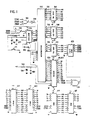
- objects in the form of cylindrical pellets 50 having frustoconical or chamfered ends move in a substantially continuous path.
- the cylindrical pellets are supplied by a source not shown, and are subsequently ground to shape by grinding wheels 51 and 52. They are then deposited in mutually spaced relationship on a first transport means, such as endless belt 53 which moves the succession of spaced-apart pellets 50 to a stacking device 54.
- the latter may comprise a pair of endless belts positioned on opposite sides of belt 53, each having a gripping surface which is disposed in a vertical plane in the drawing. The pellets are squeezed between the pair of belts so that the gripping surfaces may transport them to a stationary support located at point 55.
- pellets As the pellets arrive at the stationary support, they form stacks. As each subsequent pellet arrives the stack is urged onto a pair of rotating rollers 56 and 57. When the stack contains a predetermined number of pellets, a pusher 58 drops behind stack of pellets 59.
- the pusher is supported by a gantry 59A which is carried on rails 60 and 61.
- Motor 62 moves both gantry 59A and pusher 58 by means of a perforated steel tape 63 which engages a sprocket 64.
- Rotating rollers 56 and 57 impart a rotational motion to the stack of pellets so that the pellets, which also translate in the axial direction, are caused to spiral past an inspection station 66 which views all pellets as they pass through a viewing region 66A.
- an inspection station 66 which views all pellets as they pass through a viewing region 66A.
- Pusher 58 then pushes the stack of pellets 59 off the pair of rollers 56 and 57 and onto a second transport means, such as endless belt 67.
- Belt 67 travels at a higher linear velocity than pusher 58 so that a space is created between successive pellets.
- the belt transports the spaced pellets through a passage 68 in a turret sorter.
- the sorter wheel 69 of the sorter operates in response to information obtained by the present invention from the optical inspection of the pellets by the inspection station 66.
- Rotation of the sorter wheel 69 serves to knock the pellet present in the lowermost passage 68 into either chute 70 or 71, depending on the direction of rotation of the wheel. If the wheel does not rotate, belt 67 transports the pellets unimpeded through lowermost passage 68 to a pair of endless belts 72 and 73. The latter belts grip opposite sides of the pellets and move them to a collection station, such as a tray loader mechanism 74.
- the pellets are optically inspected as they spiral past the inspection station.
- a second pusher 81 operates alternately with first pusher 58 so that, at the time when the first pusher returns to the position indicated by numeral 82 after having pushed a stack of pellets 59 along rollers 56 and 57, the second pusher is pushing the subsequent stack of pellets past inspection station 66.
- the pellet throughput is maintained at a relatively high level.
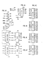
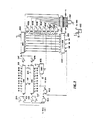
- Inspection station 66 includes optical scanning and detection apparatus such as that illustrated in greater detail in Figures 28 and 29.
- a light source 300 which is preferably a multimode laser, provides a light beam 306.
- the light beam is reflected by reflector 308 and prism 310 and is directed to a diverging lens 312 which diverges the beam.
- beam 306 is reflected by a reflector 314 and is transmitted to a collimation lens 316 which reduces the degree of divergence.
- a convergence lens 318 converges the light beam in a direction different than the direction of divergence to project an elongated light beam upon a first region of illumination 320 within the aforesaid viewing region 66A.
- the pellets of stack 50 which are present in the first region of illumination and supported by rollers 56 and 57, spiral past the first region of illumination.
- Light reflected from the surface of the pellets is collected by a lens 322 and focused onto a 1 x 1024 photodiode array 324.
- Each diode in the array corresponds to a known subregion in the first region of illumination and the light striking the photodiode contains information as to the surface characteristics of the pellet at that subregion.
- the photodiode signals are fed to data pre-processing circuitry (not shown) for evalua-. tion and data compression prior to processing by subsequently connected data processing apparatus.
- a second light source 300A producing a light beam 306A may be provided, which is reflected and focused in a manner symmetrical to that of light beam 306.
- a second illumination means shown in Figure 29, which comprises multi-mode laser 350 that projects a light beam 353.
- Beam 353 is reflected by reflectors 355 and 357 and is diverged by a diverging lens 359.
- a collimation lens 361 reduces the amount of divergence and directs the beam to reflector 363 and thence to rollers 56 and 57.
- Each of the rollers contains a slit 368.
- an object such as a pellet 369
- it will block (or eclipse) a portion of this light beam.
- an eclipsed portion 371 appears in this region of the light beam, as well as two portions 373 and 374 which contain light transmitted above and below the pellet respectively.
- a reflector 376 directs the transmitted portions to a lens 378 which collects and focuses the portions of the light beam onto a photodiode array 380.
- the cross sectional height of pellet 369 i.e. its diameter, is indicated by the height of the eclipsed portion 371.
- This information is contained in the data derived from the signals produced by individual photodiodes of photodiode array 380, the derivation being accomplished by data pre-processing circuitry (not shown).
- CPX the logical inverse of a signal
- the lead carrying this signal is similarly designated.
- CPX * the inverted signal and the lead carrying it are designated CPX *. This convention is adopted for all signals and leads illustrated and called out herein.
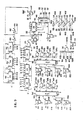
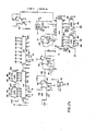
- Figure 16 illustrates circuitry when generates timing and other synchronizing pulses.
- Strobe STB31 causes the binary number, herein called "pulse frequency control number" which is present at the inputs of latches 200 and 203, to be fed to bit-rate multiplier 218.
- Bit-rate multiplier 218 functions to divide the pulse frequency control number by 64 and to multiply the quotient by the frequency of a pulse train present at lead CPX *.
- the frequency of this latter pulse train is of the order of 10 MHz and it is generated by circuitry described below.
- the resulting divided-and- multiplied signal is fed to counter 253 which further divides it by 16 and feeds the resulting signal to differential line driver 271.
- the latter applies a driving signal to the stepping motor which is of a frequency initially determined by the pulse frequency control number.
- the outputs of'counters 253, 256 and 259 are fed to NAND gate 262 and thence to flip flop 265 which triggers a one-shot multivibrator 268 to provide a timing pulse train of known frequency on lead marked PCOUNT. It also provides a timing pulse train via a buffer 274 to a lead marked DIA POS COUNT.
- Strobe STB32 functions to feed the binary number present at leads AB0 - AB7 of the AB bus through latches 206 and 209 to counters 221 and 224, respectively.
- Strobe STB33 similarly functions to feed the binary number present at leads ABO - AB7 through latches 212 and 215 to counters 227 and 230 respectively.
- These counters function to divide the frequency of the pulse train produced by bit rate multiplier 218 by the numbers fed to the counters from latches 206, 209, 212 and 215. The resulting pulse train of known frequency appears at output 6 of NAND gate 237.
- Strobe STBD is connected to the clocking input of flip flop 246 and functions to toggle flip flop 246 so as to delete a pulse on lead VELP. Thus, the frequency of the signal present at lead VELP is reduced.
- Strobe STBC is connected to the input of flip flop 249 which toggles flip flop 243. This toggling action functions to add a pulse to the lead VELP to increase the frequency of the pulse train present at lead VELP.
- Signals present on leads STBC and STBD are controlled by a microprocessor described below. Accordingly; the circuitry of Figure 16 generates timing pulses of controllable frequency at leads VELP, PCOUNT, DIA POS COUNT, and at the output of differential line driver 271.
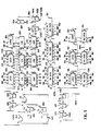
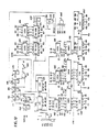
- Figure 25 illustrates circuitry utilized to process incoming photodiode signals.
- the input of buffer amplifer 290 is connected to resistors 293, 296 and 299.
- the output of each photodiode in the diode array is fed sequentially to resistor 299 by circuitry not shown.
- RAM 320 comprises individual RAMS 320a - 320h whose address inputs; namely leads 2 - 13; are connected in parallel so that all individual RAMS 320a - 320h are addressed identically.
- the analog voltage of each diode which is fed to resistor 299 in Figure 25; is amplified and buffered by three buffer amplifiers 290, 301 and 304.
- the succession of diode voltage signals produced is termed a video signal.
- the analog voltage is changed from analog form to digital form by flash converter 307. It is held by latch 310 and written as a 6-bit number onto leads AD ⁇ - AD5 and into RAM 320 at an address selected by the pair of tri-state buffers 323 and 326.
- the address is fed to these tri-state buffers by leads R ⁇ - R9.
- the address on leads R ⁇ - R9 is selected by virtue of strobe STB6 which toggles flip flops 350, 353 and 359.
- This action loads RAM 320 with data present at leads AD ⁇ - AD5, at addresses given by R ⁇ - R9 rather than at addresses given by AR0 - AR9.
- lead EOS in Figure 25 toggles flip flop 316 to activate switch 319 to discharge capacitor 380.
- strobe STB7 toggles flip flops 350, 353 and 359 to enable tri-state buffers 329 and 332 and disable tri-state buffers 323 and 326. Further, it allows data stored in RAM 320 at addresses given by leads AR ⁇ - AR9, to be read out into latches 338 and 341 and thence to tri-state buffers 344 and 347 which supply the digital data to leads DB ⁇ - DB7.
- leads marked TlVIDEO and TKVCORRL which are stored in RAM 320 and which are read out at DB6 and DB7 respectively, are discussed below.
- FIG 22 illustrates a random access memory (RAM) 400 which is used to store diode weighting factors.
- RAM 400 comprises several separate RA M 's 400a - 400h, the address leads of which are connected in parallel.
- Leads MACK and VFTM are each connected to an input of a NAND gate 431, the output of which is coupled to an input of NAND gate 434 through an inverter 437.
- the other input of NAND gate 434 is connected to lead MWDC.
- the output of NAND gate 434 is connected to RAM 400. This circuitry must be viewed in connection with that of Figure 9.
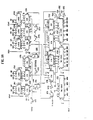
- Figure 9 depicts the fundamental diode address generator, as well as data formatting circuitry.
- the most significant bit of counters 450, 453 and 456 is connected to the input of inverter 459, the output of which is fed back to enabling inputs of counter 450.
- the most significant bit of counters 450, 453 and 456 is also connected to the enabling inputs of counters 465, 468 and 471.
- the output of gate 474 is connected to resetting input of a flip flop 477, an output of which is connected to counter 480.
- the outputs of counter 480, as well as an output of flip flop 477, is connected to inputs of a one-to-eight decoder 483.
- the outputs of this decoder are connected to leads SS0 - SS7 *.
- Leads FD ⁇ - FD7 are each connected to a clocking input of each of flip flops 498a - 498h. Leads RSS ⁇ * - RSS7 * are similarly each connected to each of a clearing input of these flip flops.
- Figures 1A through 1F and Figures 2A through 2F depict decoders which perform strobing functions and drivers that function to accommodate integrated circuit fan-out.
- One-of- eight decoders 650a - 650i are effective to decode signals present on leads AR0 - AR7, AR3 * , AR4 * , SEL0, SEL1, and SEL2 to information transmitted on strobe leads STB ⁇ - STB47 (hexadecimal notation).
- Each diode in the photodiode array may possess a different response characteristic and, further, the light reflected to each may vary in intensity from light reflected to others but due to factors unrelated to pellet surface features. Thus, it is desired to normalize all diode response characteristics and this is done by the generation of diode weighting factors.
- microprocessor 550 issues a signal through tri-state buffers 595, 598 and 601 to the AR bus, which is fed to the address selection terminals of RAM 320 through tri-state buffers 329 and 332.
- the corresponding diode signal voltage magnitude is read out of RAM 320 on the DB bus and is transmitted to microprocessor 550 for processing through tri-state buffers 686 and 689 in Figure lA, to the DB bus, and thence to the D bus through decoders 680 and 683.
- the microprocessor processes these diode signals to compute diode weighting factors as explained below.
- Microprocessor 550 is programmed by instructions contained in EPROMs 620 and 623 and RAMs 614 and 617 in Figure 1. A portion of the instructions require it to compute a weighting factor for each diode by comparing each diode signal with a predetermined norm and to generate in response a weighting factor indicative of the difference so that the diode will produce a-signal of known magnitude in response to light of a fixed intensity. After computation, these weighting factors are transmitted from microprocessor 550 through decoder 605 to the D bus, through direction control buffers 680 and 683, and along the DB bus to the bidirectional tri-states 419 and 422 in Figure 22.
- Figure 4A depicts automatic gain control circuitry used to normalize acquired pellet data.
- the operation of the circuit, illustrated in Figure 4A is as follows:
- comparator 759 indicates whether the weighted magnitude signal contained on leads AD0 - AD5 is greater than the reference magnitude contained on leads BB0 - BB7. If so, flip flop 762 is toggled, thereby advancing counters 765 and 777. These counters count upward from a number strobed into them by strobe STB1F through latches 768 and 771 and originating on the BB bus from microprocessor 550. When the output of counters 765 and 774 reaches the count of 255, flip flops 777 and 780 are toggled and signal T3STS * is fed back to microprocessor 550.
- microprocessor 550 adjusts the amplification, or gain, of the diode signals.
- the microprocessor is programmed to perform the gain adjustment approximately five times during the scanning of each pellet.
- the output of D/A converter 809 is a current which corresponds both to the weighting factor and to the gain control signal. This current is changed to a voltage by operational amplifier 812, which produces an output voltage signal that is fed to an input of flash A/D converter 307.
- Flash converter 307 also receives as an input a signal for each diode originating at resistor 299 and processed by buffer amplifiers 290, 301 and 304. Converter 307 responds with a signal on leads TDC ⁇ - TDC5, which is indicative of the diode signal magnitude but modified by the automatic gain control signal and the diode weighting factor. This signal is present on the TDC bus and is latched by latches 310 and 313 which feed the signal to leads AD0 - ADS.
- a signal termed a modified video signal, is produced on the AD bus which is indicative of the reflectivity of the inspected pellet surface, yet normalized to adjust for variations in photodiode response characteristics and for variations in the general reflectivity of the pellet surface.
- comparators 868, 871 and 874 compare the number present on the TG bus with the signal present on leads R0 - R9.
- the signal present on this R bus indicates the address of the present diode whose signal is being processed. If the diode address is a lower number than that present on the TG bus, flip flops 877 and 880 remain untoggled and the signals present at leads START * , TRACK and TRACK * indicate that the track gate is not yet operative.
- the output of comparator 874 toggles flip flop 877 and the leads START * , TRACK and TRACK * indicate that a track gate is now in existence.
- a group of successive diode signals is selected which span the length of exactly one pellet.
- counters 916, 921 and 922 begin counting upward from the number present on the TG bus and produce an output which is fed to tri-state buffers 925, 928 and 931.
- the output of the latter is fed to leads DB0 - DB7 and to leads DB0 and DB1 in two strokes.
- This output on the DB bus is fed to microprocessor 550 to provide an indication of the address of the track gate.
- the pellet On subsequent scans the pellet will have been advanced laterally, that is, axially along the roller supports, to a position such as that indicated by pellet 949, shown in ghost outline.
- the number fed by counters 859, 862 and 865 to the TG bus is advanced according to the pellet's axial velocity by signals present on leads VELP, SSX and Cl to increase the number fed to comparators 868, 871 , and 874 by way of the TG bus. This changes the track gate's beginning address to one corresponding to the new position of the pellets.
- counters 859, 862 and 865 would be incremented upward from the number strobed into them on the AB bus by signals present on leads VELP, SSX or Cl. This process will increment the number present on the TG bus to a number such as 650 shown in the drawing, such that the track gate will begin at diode 650. Diodes 1 - 649 will not be processed by the processing circuitry and only signals from diodes having addresses greater than 649 will be considered. Other circuitry described later determines the address at which the track gate is terminated so that diodes beyond the other edge of the pellet, such as 951 - 1024 with respect to pellet 946, will not be processed.
- Tri-state buffers 907, 910 and 913 function to format data present on the TG bus and translate it to data of another form for transmission to the microprocessor on the MB bus.
- the beginning of the track gate determines the lowest address of diodes whose signals are to be processed. The lowest address is changed to accommodate pellet motion along the track so that each of the 220 scans off each pellet begins at the same distance from the pellet's end, regardless of the pellet's translation along the track.
- Figure 4 depicts circuitry which provides an address, measured from the beginning address of the track gate, of each diode whose signal is being processed.
- the operation -of the circuit shown in Figure 4 is as follows:
- the now-incrementing outputs of counters 950, 953 and 956 are compared with the fixed outputs of latches 977, 980 and 983 by means of comparators 965, 968 and 971.
- the comparison determines whether the address of the diode currently being read has exceeded the length of the track gate. If so, flip flop 1004 toggles and produces a signal on lead ENDTRACK * which indicates the and of the track gate. Thus, diodes having higher addresses will not be read.
- tri-state buffers 989, 992 and 995 are strobed by lead RSS3 *.
- the track gate length latched into latches 977, 980 and 983 is fed to leads MB0 - MB15.
- Tri-state buffer 974 contains data identity information. If a particular event occurs in the signal of a diode whose address is being read, a signal at lead TRSTN * will strobe tri-state buffers 959, 962 and 974. As a result, the address of that diode and data identity information are fed to leads MB0 - MB15. This address information is used in the analysis of the diode signals as discussed below. Thus, Figure 4 depicts circuitry which provides the address of each diode whose signal is being read and the address is given with reference to the track gate address as the origin.
- Figure 5 depicts circuitry utilized to determine whether the output of each photosensitive diode exceeds each of three predetermined threshold magnitudes. Circuitry is also shown which counts the number of times a particular threshold is exceeded. The operation of the circuit of Figure 5 is explained as follows:
- the operation is similar in determining the existence of a diode voltage which exceeds a second threshold.
- a threshold term T2 indicated on the AB bus, is strobed into latches 1025 and 1028 by strobe STB2A. This data is fed to comparators 1031 and 1034 and is compared with the weighted diode values present on the AD bus. Should the actual weighted diode values exceed the threshold, flip flop 1037 is toggled and leads T2VIDEO and T2VIDEO * acquire logic values indicative of the occurrence.
- a third threshold is strobed into latches 1040 and 1043 by stobe STB3B from the data present on the AB bus.
- This latter data is fed to comparators 1046 and 1049, which compare the magnitude of threshold T3 with that of the actual weighted diode values present on the AD bus, If the actual diode values exceed the threshold, flip flop 1052 is toggled provided it is enabled by lead TRACK. The toggling action causes a signal to be fed to counter 1055 which, together with counter 1064, begins counting at the number latched into the counters by latches 1058 and 1061.
- counters 1055 and 1064 are incremented upward from the numbers latched into them by latches 1058 and 1061.
- counters 1055 and 1064 count u p to the count 255 and then feed back through the output of NOR gate 1070 and reset themselves at that time.
- the disappearance of the track gate causes the output of the NOR gate 1070 to reload counters 1055 and 1064 in preparation for the reappearance of the track gate during a subsequent scan.
- flip flop 1067 is toggled, provided it is enabled by lead ENBLDAT. This forces lead T3STB * to a logic state indicative of the occurrence of a specified number of diode excursions past threshold T3.
- the specified number is equal to 255 minus the number latched by latches 1058 and 1061.
- Threshold T3 is relatively high and is taken to indicate the receipt by a diode of light which is sufficiently bright that it must have been produced by a shiny metal object, as for example, a metal inclusion in the pellet inpsected. These occurrences are counted by counters 1055 and 1064. When a predetermined number of them has occurred, namely 255 minus the latch number of counters 1058 and 1061, a metal inclusion is deemed to exist. The latter condition is indicated by the logic state of lead T3STB * caused by the toggling of flip flop 1067. The signal T3STB * is further analyzed by circuitry discussed below:
- latches 1128 and 1131 which are strobed by strobe STB37, feed the data contained on leads BB0 - BB7 (from driver 650 in Figure 2) to inputs of comparators of 1122 and 1125.
- the data present on this BB bus indicates a predetermined number of T1VIDEO * events.
- the occurrence of each TlVIDEO * event is indicated by a logic swing of the same lead T1VIDEO * , which is connected to an input of NAND gate 1110.
- the output of the latter gate provided input C4 is of a correct logic state to enable the output to appear, reflects the occurrence of the logic swing of lead T1VIDEO *.
- lead INCRTKV undergoes a corresponding logic swing.
- This latter swing serves to increment counters 1116 and 1119, thus increasing by one the number present on leads TKV ⁇ - TKV7.
- This TKV bus is connected simultaneously to inputs of comparators 1122 and 1125 and to data inputs of RAM 1107.
- a number is read out of an address in RAM 1107, it is fed into counters 1116 and 1119. It may or may not be incremented by one of these counters due to a signal on lead INCRTRV.
- the number, incremented or not, is then fed back to. the same address, thereby storing the number of T1VIDEO events occurring at the corresponding address on the diode array.
- counters 1093, 1097 and 1104 increment through all diode addresses whose signals are analyzed. These counters repeat this cycle for each pellet scan. It is assumed that at diode number 20, for example, in each scan a dark space occurs. Thus, as counters 1093,.1097 and 1104 increment from ⁇ to 19, the TKV data input bus to the RAM stores zero at each address, since no signal appears on lead INCRTKV. However, at address 20 of the first scan a signal appears on INCRTKV and a number 1 appears on the TKV bus.
- This number is stored at address 20 in the RAM and the signal on lead INCRTKV increments counters 1116 and 1119 from zero to one.
- the counters 1093, 1094 and 1104 increment to the end of the track gate, e.g. number 400, and then restart at zero for the second scan. Again, nothing occurs on lead INCRTKV between addresses 1 to 19. However, at address 20 a signal appears on this lead and increments counters 1116 and 1119 from the number stored in RAM 1107 at address 20, namely, one to two. Thus, the number "2" appears on bus TKV and this number is fed back and stored as a "2" at the address 20 in the RAM. Again, zeroes will be stored at addresses 21 - 400. The process is carried out for 220 scans for each pellet, storing zeros at all addresses between ⁇ and 19; storing the scan number, which is 220 at the end of all scanning at address 20; and storing zeros at addresses 21 through 400.
- the existence of the interface is determined by comparing the number held on the TKV bus with that latched by the BB bus. While each pellet will be scanned 220 times, it is not considered necessary that an INCRTKV signal occur at the same address in every scan for an interface to exist. In the example above, the occurrence of perhaps 175 signals on lead INCRTKV at address 20 would be sufficient. The number considered sufficient is present on the BB bus latched by latches 1128 and 1131. When the count of INCRTKV events occurring at a given address reaches that number, comparators 1122 and 1125 issue a signal to flip flop 1137. This action toggles outputs TKVCORRL and its complement, to indicate the existence of a correlation at the address in RAM 1107 from which the number is read.
- Figure 12 illustrates circuitry for determining the address at which the interface correlation is found to occur. The operation of the circuit shown in Figure 12 is as follows:
- NAND gate 1177 functions to disable counters 1165 and 1174 in the event that excessive correlations occur, as may be mistakenly the case when a region is considered too long to be meaningful.
- Counter output leads WDl - WD6 are connected such that the binary number appearing thereon is exactly half the number stored in the counters. The width number of the interface is divided by two because only half of it is ascribed to the pellet under examination. The other half is attributed to the abutting pellet. This number is fed into binary address adders l189 and 1192 which substract it from the number latched into latches 1180, 1183 and 1186. The resulting number is fed into shift registers 1198, 1201, and 1204.
- the half-width information present on the WD bus is fed into shift registers 1204 and 1207. Accordingly, this circuit counts the number of addresses at which sufficient correlations occur to warrant the conclusion that an interface exists. The number of correlations is divided by two and subtracted from the actual diode address at the beginning of the track gate. The resulting address, indicating the actual address of the interface, together with the half-width information is available for use by other circuitry at the PI bus which constitutes the output of the shift registers.
- Figure 13 illustrates circuitry utilized to strobe data present on the PI bus into the DB bus and circuitry used to limit the areas on a pellet over which interface correlations are sought.
- the operation of the circuit of Figure 13, taken together with the pertinent portion of the circuit shown in Figure 12, is as follows:
- the number contained on the AB bus which is latched into latches 1268 and 1271 by strobe STB36 is the number at which down-counters 1274, 1277 and 1281 begin to count down when enabled by lead ICG.
- the down-counters are decremented at intervals determined by the timing of C2 * , which is in time-displaced phase with the rate of diode address changes.
- the logic state of lead STPICG * changes and the signal channge is coupled to flip flop 1225 in Figure 12.
- Lead STPICG * sets flip flop 1225 and thereby controls flip flop outputs ICG and ICG *.
- Flip flop 1225 is toggled by comparators 1216 and 1219, operating through flip flop 1222.
- comparators compare the address of the diode whose signal is currently being processed with the diode number latched in latches 1210 and 1213. When the address of the diode signal being processed exceeds that in latches 1210 and 1213, flip flop 1225 toggles. Leads ICG and ICG * are then used to terminate the search for interface correlation.
- interface correlation inquiry is only undertaken with respect to diode addresses above those latched into latches 1210 and 1213 of Figure 12 and below those latched into latches 1268 and 1271 of Figure 13. Therefore, in searching for correlation over a limited region of a pellet, the situation of searching a region longer than a pellet with the accompanying possibility of finding correlations of both ends rather than one is eliminated.
- the microprocessor 550 is programmed to establish imaginary interfaces indicating the leading edge of the first pellet and the trailing edge of the last pellet in the stack. This is done in conjunction with external optical transducers which indicate that the first or last pellet is approaching. The microprocessor then establishes the proper interface.
- Figure 6 illustrates circuitry used to determine correlations between successive scans and to report the addresses of changes in correlation. The operation of the circuit of Figure 6 is as follows:
- RAM 1328 Assuming that RAM 1328 is used, the data just stored in RAM 1328 is now used as reference data to determine the existence of correlations between it and data from subsequent scans.
- tri-state buffers 1316, 1307, 1304 and 1319 are triggered to load the data from the next scan into the other RAM, namely RAM 1331.
- Data from RAM 1328, which now comprises the reference scan is sent through tri-state buffer 1334 into shift register 1337 at a rate determined by the clocking of lead C3 *.
- Each data bit progresses along the outputs of shift register 1337 from left to right and is progressively applied to each input of EXCLUSIVE-OR gates 1325a - 1325h, beginning with lowermost EXCLUSIVE-OR gate 1325h.
- the signal present on lead TlVIDEO is transmitted to delay means 1322 which delays the signal, preferably by four pulses of the signal on lead C3 * , and then transmits it by means of lead 6 of the delay means to all the other inputs of EXCLUSIVE-OR gates 1325a - 11325h.
- the signal on lead T1VIDEO which indicates whether a particular diode output in the current scan exceeds threshold T1 is compared simultaneously with all of the signals of the four preceding diodes in the array, as well as to the signals of the four succeeding diodes by EXCLUSIVE-OR gates 1325a - 1325h.
- the existence of correlation is shown by the logic state of lead T1CORR which is connected to an output of flip flop 1346.
- Figure 18 illustrates a memory buffer used to store correlation data.
- inverters 1384a - 1384h and of buffers 1385a - 1385h are connected to peripheral devices not shown which are utilized for purposes such as data display.
- the cut- put of NAND gate 1391 is also connected to the peripheral display circuitry.
- Figure 17 illustrates a circuit used to control the data reading and writing of RAM 1375 of Figure 18.
- Figure 8 illustrates circuitry used to control data formatting in connection with the loading and unloading of RAM 1375 in Figure 18.
- the diode address is stored in RAM 1375.
- the diode signals reported during the duration of the artifact are not stored because they are deemed redundant.
- the next signal which is stored is that from the diode at which the artifact stops and this diode address is stored in RAM 1375. Therefore, a linear artifact of a width equal to that of the width scanned by the photodiode array, will be recorded in RAM 1375 as two addresses, namely the beginning and the end.
- a rectangular artifact of substantial width will be recorded by the diode addresses and scan numbers of its four corners, and so on.
- Figure 7 illustrates circuitry utilized to determine the existence of the correlation of events at which diode signals exceed the T2 video threshold. The operation of the circuitry of Figure 7 is similar to that of the corresponding circuitry of Figure 6 and need not therefore be further described.
- Figure 14 illustrates a circuit for tallying areas of missing pellet surface. The operation of the circuit shown in Figure 14 is as follows:
- latches 1726, 1728 and 1730 are fed to down-counters 1720, 1722 and 1724 which begin counting at the time the missing surface gate comes into existence. They are clocked by lead Cl and for the interval during which they count from the number fed to them by latches 1726, 1728 and 1737 to the number zero, the missing surface gate is kept in existence.
- a signal fed to flip flop 1711 toggles the flip flop and thereby prevents counting of TlVIDEO events by counters 1735, 1738, 1741 and 1752.
- the output of counters 1735, 1738, 1741 and 1752 is indicative of the total number of TlVIDEO events which occurred.
- the number contained in these four counters is transmitted to leads MB ⁇ - MB11 by means of tri-state buffers 1744 and 1747.
- Information from tri-state buffer 1750 is fed to leads MB12 - MB15 and identifies the information on leads MB ⁇ - MB11 as missing surface data.
- Figure 15 illustrates a circuit which generates a number to be associated with data corresponding to each pellet for identification of the data and, further, to generate a number identifying the scan which is producing the data.
- the scan number accordingly gives a circumferential coordinate while the diode address gives an axial coordinate.
- these two corordinates may refer to a diode currently being scanned or to the signal of a diode stored in memory.
- the operation of the circuit shown in Figure 15 is as follows:
- Lead PRSTPC * presents counters 1779, 1781, 1794 and 1796 to the numbers latched into them by latches 1775, 1777, 1790 and 1792. Beginning with this number, counters 1779, 1781, 1794 and 1796 count upward, as clocked by signals on lead Cl *.
- a unique number is provided which can be associated with each pellet in the pellet string; and data being processed by other circuitry can be associated with the pellet to which the data belongs.
- Figure 10 illustrates a circuit which counts scan numbers to determine whether a full pellet has been scanned; which feeds data identity information to be associated with certain data transmitted on the MB bus; and which strobes pellet position count data to the DB bus for the microprocessor to use.
- the operation of the circuity of Figure 10 is as follows :
- a signal present on lead STB27 functions to strobe the number contained in latches 1830 and 1832 into comparators.1834 and 1836, to be compared with the actual scan number fed to comparators 1834 and 1836 by leads SC0 - SC7.
- flip flop 1838 is toggled and produces a signal on lead EOP * which indicates that a full pellet has been scanned.
- the binary number contained in latches 1830 and 183-2 is decimal 220.
- Leads RSS6 * and RSS * trigger tri-state bufffer 1846 to transmit the four-bit word present at leads 2, 4, 6 and 10 to leads MB12 - MB15 respectively. This information is transmitted on other leads of the MB bus to identify the information on the other leads.
- Signals present on leads STB46 and STB47 strobe information present on the PC bus into the DB bus at two different times.
- Figure 23 depicts circuitry which converts the digital output of flash A/D converter 307 in Figure 25, as well as the digital values of thresholds T 1 , T 2 and T 3 , into analog signals and multiplexes the signals for transmission to an oscilloscope.
- the output of operational amplifier 1897 is connected to a terminal 1905 through resistor 1907.
- Terminals 1905 and 1920 are adapted to be connected to display and triggering inputs of an oscilloscope [not shown].
- Drivers 1925 and 1926 function to start the scanning sequence of the photodiode array and to supply the array with clock pulses.
- the operation of the circuitry of Figure 23 is as follows:
- Figure 24 illustrates pusher detector circuitry. Two circuits are shown, namely those of Figure 24A and Figure 24B. These are substantially identical except for the fact that the input of Figure 24A is connected to pusher 1 and the input of Figure 24B is connected to pusher 2. Further, the output of the circuit of Figure 24A is designated PSHR1 * , while the output of the circuit of Figure 24B is designated PSHR2 *.
- the operation of the circuit of Figures 24A and 24B is as follows:
- the metal body of one of the two pushers [not shown] approaches a transducer [not shown] which may comprise an eddy current coil fixed to a stationary support.
- This action causes a signal to be applied to node 1957 and thence to LED 1958.
- Light produced by LED 1958 is transmitted to the phototransistor and serves to modulate the current flowing through resistor 1965, to produce a voltage signal at node 1962 which is indicative of the position of the pusher.
- Diode 1955 protects LED 1958 in the event that an excessive voltage is applied to node 1957.
- the use of LED 1958 and phototransistor 1960 isolates the signal produced at node 1962 from noise present at node 1957.
- circuitry of Figure 24B is substantially the same, but is applicable to the other pusher.
- Figure 4B depicts circuitry which generates operating signals to an external transducer.
- the successful sending or receipt of selected signals on the BBB bus is indicated by the output of the SSD's.
- the output is indicative of the signals present on leads BB ⁇ - BB3 and the output is coded to indicate the type of signal sent or received on the bus.
- Figure 19 depicts circuitry for generating signals available to an operator which indicate the operation of preprocessor circuitry.
- the following leads herein termed “monitoring leads”, namely, LEDTRACK * , TS ⁇ *, XFRENBL * , 8KEMPTY, 8KOVFL * , SYSMEM * MS4 * , MS8 * , LEDTRACK * , TKVCORRL, TlVIDEO, T2VIDEO, T3VIDEO, MSG * , and ICG * , are connected to inputs of inverters 2050a - 2050p respectively.
- the signals on some of the monitoring leads are manifest as optical signals by light emitting diodes 2054a - 2054i.
- the signals on the rest of the monitoring leads are transmitted to leads TPl - TP7 for connection to external monitoring circuitry.
- the inverters interposed between the CP bus and the C bus function to invert signals on the CP bus, as well as to provide current sources to accomodate circuit fan-out.
- Figure 21 illustrates circuitry comprising the executive controller. The operation of the circuitry of Figure 21 is as follows:
- FIFO's 2142 and 2144 function in a symmetrical manner to store in parallel eight-bit groups of data inputted by the DB bus and to then feed the data to inverters 2170a - 2170h.
- FIFO's 2142 and 2144 contains information relevant to sorting actions to be taken with respect to the pellets.
- Figures 30, 31 and 32 illustrate circuitry utilized in conjunction with photodiode array 380 in Figure 29 to make diameter measurement computations.
- the operation of the circuits of Figures 30, 31 and 32 is as follows:
- Leads CP1, CP1 * , CP2 and CP2 * feed signals to the counters in Figure 31 to thereby indicate the positions of transmitted light beams 373 and 374 in Figure 29 in terms of diode addresses of photodiode array 380.
- the length of the eclipsed region 371 and hence the pellet diameter can be determined.
- the latches may be integrated circuit chip (IC) type 74161 operated in a latching mode and the counters may be the identical type of chip operated in a counting mode.
- the microprocessor is preferably an IC type 8080A-1.
- the l-of-8 decoders may be 1C type 8205.
- the EPROMS may be IC type 2732, and RAMs 614 and 617 in Figure 1 may be IC type 2114.
- the bidirectional bus drivers may be IC type 8216.
- Oscillator 553 in Figure 1 may be an IC type 8224.
- Decoder 605 in Figure 1 may be an IC type 8228, and 8-to-1 encoder-multiplexer 692 in Figure 2F may be an IC type 74151.
- the comparators may be IC type 74585 or 7485.
- the flip flops may be IC type 7474 or 745112.
- Delay/shift registers 1322 and 1655 in Figures 6 and 7 may be IC type 74164; shift registers 1337 and 1650 in these figures may be IC type 74164. Decoders 1659 and 1313 in these figures may be IC type 74151; and the RAM's in these figures may be IC type 2125. The IC type 2125 chips may also be used for the RAM's in Figures 11, 20 and 22.
- the adders in Figure 12 may-be IC type 7483 ; and the FIFO's may be IC type 74193.
- Multiplier 218 in Figure 16 may be IC type 7497.
- Driver- amplifiers may be IC type DS8832.
- RAM's in Figure 18 may be IC type 2147.
- D/A converters may be IC type DAC08.
- Flash A/D converter 307 in Figure 25 may be IC type TDC1014J.
- Buffer/ampli- fiers 290, 301, 304 and 812 may be IC type 2520.
- Tri-state buffers may be IC type DM 8095 manufactured by National Semiconductror Corp.
- the present invention provides an automated pellet inspection system in which pellets following a substantially continuous path are spiraled past an inspection station with a high degree of mechanical stability.
- the inspection station optically inspects the pellets and associated preprocessor circuitry allows high throughput with optimum inspection reliability.
- the system allows examination of minute pellet areas.
- a data compression technique using exception reporting reduces the data rate to minimize the data processing capacity required.
- Each pellet has a diameter measurement performed on it and is inspected for roundness and the like.
- the pellets are stacked in end-to-end abutment during inspection and each pellet is identified by the interface separating it from its abutting neighbors or by the chamfered ends of the pellets. This is effected by the correlation of the locations of specific signal intensities and includes the generation of a track gate which correlates all data with the particular pellet from which it is derived.
- the reliability of inspection is further enhanced by normalizing the signals derived from the optical inspection process. These signals may vary due to factors extraneous to the pellet characteristics of interest, and the signal normalization compensates for such variations.
- the automated object inspection method, apparatus and system disclosed above is equally suitable for inspection of other cylindrical objects such as tubing, cans, bottles and the like; and lends inself to numerous modifications, changes, substitutions and equivalents; and portions of the invention may be used without the use of other portions thereof.
Landscapes
- Physics & Mathematics (AREA)
- Health & Medical Sciences (AREA)
- Life Sciences & Earth Sciences (AREA)
- Chemical & Material Sciences (AREA)
- Analytical Chemistry (AREA)
- Biochemistry (AREA)
- General Health & Medical Sciences (AREA)
- General Physics & Mathematics (AREA)
- Immunology (AREA)
- Pathology (AREA)
- Investigating Materials By The Use Of Optical Means Adapted For Particular Applications (AREA)
- Monitoring And Testing Of Nuclear Reactors (AREA)
- Length Measuring Devices By Optical Means (AREA)
- Testing Or Measuring Of Semiconductors Or The Like (AREA)
Applications Claiming Priority (2)
| Application Number | Priority Date | Filing Date | Title |
|---|---|---|---|
| US361933 | 1982-03-25 | ||
| US06/361,933 US4496056A (en) | 1982-03-25 | 1982-03-25 | Automated inspection system |
Publications (3)
| Publication Number | Publication Date |
|---|---|
| EP0090304A2 true EP0090304A2 (de) | 1983-10-05 |
| EP0090304A3 EP0090304A3 (en) | 1985-01-09 |
| EP0090304B1 EP0090304B1 (de) | 1989-03-15 |
Family
ID=23423990
Family Applications (1)
| Application Number | Title | Priority Date | Filing Date |
|---|---|---|---|
| EP83102759A Expired EP0090304B1 (de) | 1982-03-25 | 1983-03-21 | Vorrichtung zur Untersuchung von im wesentlichen runden Ojekten |
Country Status (6)
| Country | Link |
|---|---|
| US (1) | US4496056A (de) |
| EP (1) | EP0090304B1 (de) |
| JP (1) | JPS59192942A (de) |
| CA (1) | CA1206593A (de) |
| DE (1) | DE3379421D1 (de) |
| ES (1) | ES8605337A1 (de) |
Cited By (8)
| Publication number | Priority date | Publication date | Assignee | Title |
|---|---|---|---|---|
| GB2239089A (en) * | 1987-10-08 | 1991-06-19 | Elor Optronics Ltd | Small arms ammunition inspection system |
| FR2667398A1 (fr) * | 1990-09-27 | 1992-04-03 | Cogema | Procede et installation d'examen automatique de la surface circonferentielle d'objets cylindriques. |
| WO1993001493A1 (en) * | 1991-07-04 | 1993-01-21 | Marposs Societa' Per Azioni | Apparatus for checking surface features of conical parts |
| EP0597639A1 (de) * | 1992-11-12 | 1994-05-18 | Westinghouse Electric Corporation | Berührungslose Erkennung von Oberflächenfehlern |
| EP0605317A1 (de) * | 1992-12-29 | 1994-07-06 | Societe Franco-Belge De Fabrication De Combustibles Fbfc | Optisches Verfahren und Vorrichtung zur automatischen Klassifizierung zylindrischer Kernbrennstofftabletten |
| US5991017A (en) * | 1995-06-15 | 1999-11-23 | British Nuclear Fuels Plc | Inspecting the surface of an object |
| KR101050050B1 (ko) * | 2009-12-31 | 2011-07-19 | 유진인스텍 주식회사 | 로드의 결함검출장치 |
| KR101335217B1 (ko) * | 2011-09-21 | 2014-01-03 | 유진인스텍 주식회사 | 봉형상체의 결함측정장치 |
Families Citing this family (19)
| Publication number | Priority date | Publication date | Assignee | Title |
|---|---|---|---|---|
| JPS58106409A (ja) * | 1981-12-18 | 1983-06-24 | Seiko Instr & Electronics Ltd | 部品の姿勢判別装置 |
| JPH0722166B2 (ja) * | 1982-09-22 | 1995-03-08 | 株式会社東芝 | ダイボンダ等におけるペレツト認識方法 |
| US4733360A (en) * | 1984-06-14 | 1988-03-22 | Dai Nippon Insatsu Kabushiki Kaisha | Device and method for inspecting card-like articles |
| JPS6353450A (ja) * | 1986-08-25 | 1988-03-07 | Toyo Seikan Kaisha Ltd | 座屈缶の検出方法とその装置 |
| US4969746A (en) * | 1988-09-02 | 1990-11-13 | R. J. Reynolds Tobacco Company | Component inspection apparatus and method |
| US5010494A (en) * | 1988-09-09 | 1991-04-23 | North Carolina State University | Method and apparatus for detecting mechanical roll imperfections in a roller drafting system |
| US5186887A (en) * | 1990-10-02 | 1993-02-16 | Mitsubishi Nuclear Fuel Co. | Apparatus for inspecting peripheral surfaces of nuclear fuel pellets |
| ES2079299B1 (es) * | 1991-01-14 | 1998-03-01 | Westinghouse Electric Corp | Aparato para la transferencia de pastillas de combustible nuclear de configuracion cilindrica aplicable a un aparato para la inspeccion de las mismas. |
| US5147047A (en) * | 1991-01-14 | 1992-09-15 | Westinghouse Electric Corp. | Pellet inspection system |
| US5213218A (en) * | 1991-08-05 | 1993-05-25 | Westinghouse Electric Corp. | Pellet reject apparatus and method |
| US6038335A (en) * | 1995-06-05 | 2000-03-14 | Matsushita Electric Industrial Co. Ltd. | Flaw detection apparatus using digital image data indicative of a surface of an object |
| US6131817A (en) | 1998-10-09 | 2000-10-17 | Nbs Technologies, Inc. | Plastic card transport apparatus and inspection system |
| ES2207354B2 (es) * | 2001-05-25 | 2006-04-16 | Enusa Industrias Avanzadas, S.A. | Aparato para la inspeccion automatizada de la apariencia de la superficie de pastillas nucleares. |
| US7593501B2 (en) * | 2005-01-06 | 2009-09-22 | Areva Np Inc. | Segment make-up system and method for manufacturing nuclear fuel rods |
| FR2892189B1 (fr) * | 2005-10-18 | 2007-12-21 | Cogema | Tri de pastilles par mesure du diametre |
| JP5582402B2 (ja) * | 2010-11-29 | 2014-09-03 | 日立Geニュークリア・エナジー株式会社 | ガンマスキャン装置 |
| CN103765241A (zh) * | 2011-04-29 | 2014-04-30 | 怀卡托大学 | 低功率范围成像相机的谐振调制 |
| CN105118535B (zh) * | 2015-07-03 | 2017-08-29 | 中广核研究院有限公司 | 核燃料组件修复检测控制系统 |
| CN106872493B (zh) * | 2017-01-12 | 2019-09-13 | 中国原子能科学研究院 | 核燃料组件无损探测装置 |
Family Cites Families (11)
| Publication number | Priority date | Publication date | Assignee | Title |
|---|---|---|---|---|
| US3355014A (en) * | 1964-11-06 | 1967-11-28 | Trw Inc | Automatic surface flaw detector |
| US3799682A (en) * | 1972-06-16 | 1974-03-26 | K Hoadley | Apparatus for feeding polished machine parts past optical scanning means to enable inspection of the polished parts |
| USRE29839E (en) * | 1972-06-29 | 1978-11-21 | Gallaher Ltd. | Optical inspection apparatus |
| JPS502388U (de) * | 1973-05-01 | 1975-01-10 | ||
| JPS6055762B2 (ja) * | 1977-04-08 | 1985-12-06 | 株式会社日立製作所 | 円筒物体外観検査装置 |
| US4226539A (en) * | 1976-12-24 | 1980-10-07 | Hitachi, Ltd. | Cylindrical body appearance inspection apparatus |
| US4155455A (en) * | 1977-09-06 | 1979-05-22 | Magnetic Analysis Corporation | Eddy current and variable reluctance test apparatus for rollers and the like |
| US4305661A (en) * | 1979-02-27 | 1981-12-15 | Diffracto, Ltd. | Method and apparatus for determining physical characteristics of objects and object surfaces |
| US4349112A (en) * | 1980-03-31 | 1982-09-14 | The United States Of America As Represented By The United States Department Of Energy | Pellet inspection apparatus |
| DE3030140C2 (de) * | 1980-08-08 | 1984-05-03 | B.A.T. Cigaretten-Fabriken Gmbh, 2000 Hamburg | Einrichtung zur optischen Überprüfung der Oberfläche von stabförmigen Rauchartikeln und/oder Filterstäben für die Tabakindustrie |
| US4377238A (en) * | 1980-08-27 | 1983-03-22 | The United States Of America As Represented By The United States Department Of Energy | Flaw detection and evaluation |
-
1982
- 1982-03-25 US US06/361,933 patent/US4496056A/en not_active Expired - Fee Related
-
1983
- 1983-03-21 EP EP83102759A patent/EP0090304B1/de not_active Expired
- 1983-03-21 DE DE8383102759T patent/DE3379421D1/de not_active Expired
- 1983-03-24 ES ES520941A patent/ES8605337A1/es not_active Expired
- 1983-03-25 CA CA000424524A patent/CA1206593A/en not_active Expired
- 1983-03-25 JP JP58051375A patent/JPS59192942A/ja active Granted
Cited By (10)
| Publication number | Priority date | Publication date | Assignee | Title |
|---|---|---|---|---|
| GB2239089A (en) * | 1987-10-08 | 1991-06-19 | Elor Optronics Ltd | Small arms ammunition inspection system |
| FR2667398A1 (fr) * | 1990-09-27 | 1992-04-03 | Cogema | Procede et installation d'examen automatique de la surface circonferentielle d'objets cylindriques. |
| WO1993001493A1 (en) * | 1991-07-04 | 1993-01-21 | Marposs Societa' Per Azioni | Apparatus for checking surface features of conical parts |
| US5486760A (en) * | 1991-07-04 | 1996-01-23 | Marposs Societa' Per Azioni | Apparatus for checking surface features of conical parts including a probe disposed within a transversal groove of a roller |
| EP0597639A1 (de) * | 1992-11-12 | 1994-05-18 | Westinghouse Electric Corporation | Berührungslose Erkennung von Oberflächenfehlern |
| KR100301976B1 (ko) * | 1992-11-12 | 2001-10-22 | 드폴 루이스 에이 | 비접촉표면결함검출방법및장치 |
| EP0605317A1 (de) * | 1992-12-29 | 1994-07-06 | Societe Franco-Belge De Fabrication De Combustibles Fbfc | Optisches Verfahren und Vorrichtung zur automatischen Klassifizierung zylindrischer Kernbrennstofftabletten |
| US5991017A (en) * | 1995-06-15 | 1999-11-23 | British Nuclear Fuels Plc | Inspecting the surface of an object |
| KR101050050B1 (ko) * | 2009-12-31 | 2011-07-19 | 유진인스텍 주식회사 | 로드의 결함검출장치 |
| KR101335217B1 (ko) * | 2011-09-21 | 2014-01-03 | 유진인스텍 주식회사 | 봉형상체의 결함측정장치 |
Also Published As
| Publication number | Publication date |
|---|---|
| CA1206593A (en) | 1986-06-24 |
| ES520941A0 (es) | 1986-03-16 |
| US4496056A (en) | 1985-01-29 |
| JPS59192942A (ja) | 1984-11-01 |
| DE3379421D1 (en) | 1989-04-20 |
| ES8605337A1 (es) | 1986-03-16 |
| JPH033178B2 (de) | 1991-01-17 |
| EP0090304A3 (en) | 1985-01-09 |
| EP0090304B1 (de) | 1989-03-15 |
Similar Documents
| Publication | Publication Date | Title |
|---|---|---|
| EP0090304A2 (de) | Vorrichtung zur Untersuchung von im wesentlichen runden Ojekten | |
| US5101101A (en) | Method of detecting opaque foreign article from among transparent bodies utilizing polarized light | |
| US4222275A (en) | System for non-destructively acquiring and processing information about a test piece | |
| US4448532A (en) | Automatic photomask inspection method and system | |
| US4929843A (en) | Apparatus and method for determining a dimension of an object | |
| EP0315697B1 (de) | Fühler zur unterscheidung von fehlern in lichtdurchlassendem bahnförmigem material | |
| JPS6236170B2 (de) | ||
| US4253768A (en) | Processing system for detection and the classification of flaws on metallic surfaces | |
| US5311977A (en) | High resolution parts handling system | |
| EP2105216B1 (de) | Prüfvorrichtung mit Zwirbelstromprüfung | |
| CN109211921A (zh) | 一种精密五金件检测装置 | |
| US5542520A (en) | Coin testing apparatus | |
| EP0332376A2 (de) | Apparat zur Inspektion von Umbördelungen bei Blechdosen und ähnlichem | |
| JPH04290910A (ja) | カメラセンサーと走査の方法 | |
| JPH06213824A (ja) | 表面の検査方法および検査装置 | |
| JP3694590B2 (ja) | 農産物の画像読取装置及びこれを用いた選別装置 | |
| WO2003077724A3 (en) | Method for improving the accuracy of data obtained in a laser imaging apparatus | |
| US4777628A (en) | Seismic system and method | |
| EP0320529A1 (de) | Regelvorrichtung für Förderanlagen | |
| US5142591A (en) | High resolution camera with hardware data compaction | |
| JPS59157507A (ja) | 形状欠陥検出装置 | |
| CA1145928A (en) | Method and apparatus for grading fruit | |
| JP2582744B2 (ja) | 選別装置駆動用回路 | |
| JPH0612251B2 (ja) | ねじの検査装置及びその装置を用いた検査方法 | |
| JPH0562942B2 (de) |
Legal Events
| Date | Code | Title | Description |
|---|---|---|---|
| PUAI | Public reference made under article 153(3) epc to a published international application that has entered the european phase |
Free format text: ORIGINAL CODE: 0009012 |
|
| AK | Designated contracting states |
Designated state(s): DE IT SE |
|
| PUAL | Search report despatched |
Free format text: ORIGINAL CODE: 0009013 |
|
| AK | Designated contracting states |
Designated state(s): DE IT SE |
|
| RHK1 | Main classification (correction) |
Ipc: G01N 21/88 |
|
| 17P | Request for examination filed |
Effective date: 19850629 |
|
| 17Q | First examination report despatched |
Effective date: 19861020 |
|
| GRAA | (expected) grant |
Free format text: ORIGINAL CODE: 0009210 |
|
| AK | Designated contracting states |
Kind code of ref document: B1 Designated state(s): DE IT SE |
|
| REF | Corresponds to: |
Ref document number: 3379421 Country of ref document: DE Date of ref document: 19890420 |
|
| ITF | It: translation for a ep patent filed | ||
| PLBE | No opposition filed within time limit |
Free format text: ORIGINAL CODE: 0009261 |
|
| STAA | Information on the status of an ep patent application or granted ep patent |
Free format text: STATUS: NO OPPOSITION FILED WITHIN TIME LIMIT |
|
| 26N | No opposition filed | ||
| ITTA | It: last paid annual fee | ||
| PGFP | Annual fee paid to national office [announced via postgrant information from national office to epo] |
Ref country code: SE Payment date: 19920213 Year of fee payment: 10 |
|
| PGFP | Annual fee paid to national office [announced via postgrant information from national office to epo] |
Ref country code: DE Payment date: 19920410 Year of fee payment: 10 |
|
| PG25 | Lapsed in a contracting state [announced via postgrant information from national office to epo] |
Ref country code: SE Effective date: 19930322 |
|
| PG25 | Lapsed in a contracting state [announced via postgrant information from national office to epo] |
Ref country code: DE Effective date: 19931201 |
|
| EUG | Se: european patent has lapsed |
Ref document number: 83102759.4 Effective date: 19931008 |