EP0090566B1 - Empaquetage pour dispositif semi-conducteur - Google Patents
Empaquetage pour dispositif semi-conducteur Download PDFInfo
- Publication number
- EP0090566B1 EP0090566B1 EP83301536A EP83301536A EP0090566B1 EP 0090566 B1 EP0090566 B1 EP 0090566B1 EP 83301536 A EP83301536 A EP 83301536A EP 83301536 A EP83301536 A EP 83301536A EP 0090566 B1 EP0090566 B1 EP 0090566B1
- Authority
- EP
- European Patent Office
- Prior art keywords
- gold
- alloy
- silicon
- chip
- layer
- Prior art date
- Legal status (The legal status is an assumption and is not a legal conclusion. Google has not performed a legal analysis and makes no representation as to the accuracy of the status listed.)
- Expired
Links
Images
Classifications
-
- H—ELECTRICITY
- H10—SEMICONDUCTOR DEVICES; ELECTRIC SOLID-STATE DEVICES NOT OTHERWISE PROVIDED FOR
- H10W—GENERIC PACKAGES, INTERCONNECTIONS, CONNECTORS OR OTHER CONSTRUCTIONAL DETAILS OF DEVICES COVERED BY CLASS H10
- H10W70/00—Package substrates; Interposers; Redistribution layers [RDL]
- H10W70/60—Insulating or insulated package substrates; Interposers; Redistribution layers
- H10W70/62—Insulating or insulated package substrates; Interposers; Redistribution layers characterised by their interconnections
- H10W70/66—Conductive materials thereof
-
- H—ELECTRICITY
- H10—SEMICONDUCTOR DEVICES; ELECTRIC SOLID-STATE DEVICES NOT OTHERWISE PROVIDED FOR
- H10W—GENERIC PACKAGES, INTERCONNECTIONS, CONNECTORS OR OTHER CONSTRUCTIONAL DETAILS OF DEVICES COVERED BY CLASS H10
- H10W72/00—Interconnections or connectors in packages
- H10W72/30—Die-attach connectors
-
- H—ELECTRICITY
- H10—SEMICONDUCTOR DEVICES; ELECTRIC SOLID-STATE DEVICES NOT OTHERWISE PROVIDED FOR
- H10W—GENERIC PACKAGES, INTERCONNECTIONS, CONNECTORS OR OTHER CONSTRUCTIONAL DETAILS OF DEVICES COVERED BY CLASS H10
- H10W76/00—Containers; Fillings or auxiliary members therefor; Seals
- H10W76/10—Containers or parts thereof
- H10W76/12—Containers or parts thereof characterised by their shape
- H10W76/15—Containers comprising an insulating or insulated base
- H10W76/157—Containers comprising an insulating or insulated base having interconnections parallel to the insulating or insulated base
-
- H—ELECTRICITY
- H10—SEMICONDUCTOR DEVICES; ELECTRIC SOLID-STATE DEVICES NOT OTHERWISE PROVIDED FOR
- H10W—GENERIC PACKAGES, INTERCONNECTIONS, CONNECTORS OR OTHER CONSTRUCTIONAL DETAILS OF DEVICES COVERED BY CLASS H10
- H10W95/00—Packaging processes not covered by the other groups of this subclass
-
- H—ELECTRICITY
- H10—SEMICONDUCTOR DEVICES; ELECTRIC SOLID-STATE DEVICES NOT OTHERWISE PROVIDED FOR
- H10W—GENERIC PACKAGES, INTERCONNECTIONS, CONNECTORS OR OTHER CONSTRUCTIONAL DETAILS OF DEVICES COVERED BY CLASS H10
- H10W70/00—Package substrates; Interposers; Redistribution layers [RDL]
- H10W70/60—Insulating or insulated package substrates; Interposers; Redistribution layers
- H10W70/67—Insulating or insulated package substrates; Interposers; Redistribution layers characterised by their insulating layers or insulating parts
- H10W70/68—Shapes or dispositions thereof
- H10W70/682—Shapes or dispositions thereof comprising holes having chips therein
-
- H—ELECTRICITY
- H10—SEMICONDUCTOR DEVICES; ELECTRIC SOLID-STATE DEVICES NOT OTHERWISE PROVIDED FOR
- H10W—GENERIC PACKAGES, INTERCONNECTIONS, CONNECTORS OR OTHER CONSTRUCTIONAL DETAILS OF DEVICES COVERED BY CLASS H10
- H10W72/00—Interconnections or connectors in packages
- H10W72/071—Connecting or disconnecting
- H10W72/075—Connecting or disconnecting of bond wires
- H10W72/07541—Controlling the environment, e.g. atmosphere composition or temperature
- H10W72/07554—Controlling the environment, e.g. atmosphere composition or temperature changes in dispositions
-
- H—ELECTRICITY
- H10—SEMICONDUCTOR DEVICES; ELECTRIC SOLID-STATE DEVICES NOT OTHERWISE PROVIDED FOR
- H10W—GENERIC PACKAGES, INTERCONNECTIONS, CONNECTORS OR OTHER CONSTRUCTIONAL DETAILS OF DEVICES COVERED BY CLASS H10
- H10W72/00—Interconnections or connectors in packages
- H10W72/50—Bond wires
- H10W72/541—Dispositions of bond wires
- H10W72/5449—Dispositions of bond wires not being orthogonal to a side surface of the chip, e.g. fan-out arrangements
-
- H—ELECTRICITY
- H10—SEMICONDUCTOR DEVICES; ELECTRIC SOLID-STATE DEVICES NOT OTHERWISE PROVIDED FOR
- H10W—GENERIC PACKAGES, INTERCONNECTIONS, CONNECTORS OR OTHER CONSTRUCTIONAL DETAILS OF DEVICES COVERED BY CLASS H10
- H10W72/00—Interconnections or connectors in packages
- H10W72/50—Bond wires
- H10W72/551—Materials of bond wires
- H10W72/552—Materials of bond wires comprising metals or metalloids, e.g. silver
- H10W72/5522—Materials of bond wires comprising metals or metalloids, e.g. silver comprising gold [Au]
-
- H—ELECTRICITY
- H10—SEMICONDUCTOR DEVICES; ELECTRIC SOLID-STATE DEVICES NOT OTHERWISE PROVIDED FOR
- H10W—GENERIC PACKAGES, INTERCONNECTIONS, CONNECTORS OR OTHER CONSTRUCTIONAL DETAILS OF DEVICES COVERED BY CLASS H10
- H10W72/00—Interconnections or connectors in packages
- H10W72/50—Bond wires
- H10W72/551—Materials of bond wires
- H10W72/552—Materials of bond wires comprising metals or metalloids, e.g. silver
- H10W72/5524—Materials of bond wires comprising metals or metalloids, e.g. silver comprising aluminium [Al]
-
- H—ELECTRICITY
- H10—SEMICONDUCTOR DEVICES; ELECTRIC SOLID-STATE DEVICES NOT OTHERWISE PROVIDED FOR
- H10W—GENERIC PACKAGES, INTERCONNECTIONS, CONNECTORS OR OTHER CONSTRUCTIONAL DETAILS OF DEVICES COVERED BY CLASS H10
- H10W72/00—Interconnections or connectors in packages
- H10W72/90—Bond pads, in general
- H10W72/931—Shapes of bond pads
- H10W72/932—Plan-view shape, i.e. in top view
-
- H—ELECTRICITY
- H10—SEMICONDUCTOR DEVICES; ELECTRIC SOLID-STATE DEVICES NOT OTHERWISE PROVIDED FOR
- H10W—GENERIC PACKAGES, INTERCONNECTIONS, CONNECTORS OR OTHER CONSTRUCTIONAL DETAILS OF DEVICES COVERED BY CLASS H10
- H10W72/00—Interconnections or connectors in packages
- H10W72/90—Bond pads, in general
- H10W72/951—Materials of bond pads
- H10W72/952—Materials of bond pads comprising metals or metalloids, e.g. PbSn, Ag or Cu
-
- H—ELECTRICITY
- H10—SEMICONDUCTOR DEVICES; ELECTRIC SOLID-STATE DEVICES NOT OTHERWISE PROVIDED FOR
- H10W—GENERIC PACKAGES, INTERCONNECTIONS, CONNECTORS OR OTHER CONSTRUCTIONAL DETAILS OF DEVICES COVERED BY CLASS H10
- H10W90/00—Package configurations
- H10W90/701—Package configurations characterised by the relative positions of pads or connectors relative to package parts
- H10W90/751—Package configurations characterised by the relative positions of pads or connectors relative to package parts of bond wires
- H10W90/754—Package configurations characterised by the relative positions of pads or connectors relative to package parts of bond wires between a chip and a stacked insulating package substrate, interposer or RDL
-
- H—ELECTRICITY
- H10—SEMICONDUCTOR DEVICES; ELECTRIC SOLID-STATE DEVICES NOT OTHERWISE PROVIDED FOR
- H10W—GENERIC PACKAGES, INTERCONNECTIONS, CONNECTORS OR OTHER CONSTRUCTIONAL DETAILS OF DEVICES COVERED BY CLASS H10
- H10W90/00—Package configurations
- H10W90/701—Package configurations characterised by the relative positions of pads or connectors relative to package parts
- H10W90/751—Package configurations characterised by the relative positions of pads or connectors relative to package parts of bond wires
- H10W90/756—Package configurations characterised by the relative positions of pads or connectors relative to package parts of bond wires between a chip and a stacked lead frame, conducting package substrate or heat sink
-
- Y—GENERAL TAGGING OF NEW TECHNOLOGICAL DEVELOPMENTS; GENERAL TAGGING OF CROSS-SECTIONAL TECHNOLOGIES SPANNING OVER SEVERAL SECTIONS OF THE IPC; TECHNICAL SUBJECTS COVERED BY FORMER USPC CROSS-REFERENCE ART COLLECTIONS [XRACs] AND DIGESTS
- Y10—TECHNICAL SUBJECTS COVERED BY FORMER USPC
- Y10S—TECHNICAL SUBJECTS COVERED BY FORMER USPC CROSS-REFERENCE ART COLLECTIONS [XRACs] AND DIGESTS
- Y10S228/00—Metal fusion bonding
- Y10S228/904—Wire bonding
-
- Y—GENERAL TAGGING OF NEW TECHNOLOGICAL DEVELOPMENTS; GENERAL TAGGING OF CROSS-SECTIONAL TECHNOLOGIES SPANNING OVER SEVERAL SECTIONS OF THE IPC; TECHNICAL SUBJECTS COVERED BY FORMER USPC CROSS-REFERENCE ART COLLECTIONS [XRACs] AND DIGESTS
- Y10—TECHNICAL SUBJECTS COVERED BY FORMER USPC
- Y10T—TECHNICAL SUBJECTS COVERED BY FORMER US CLASSIFICATION
- Y10T29/00—Metal working
- Y10T29/49—Method of mechanical manufacture
- Y10T29/49002—Electrical device making
- Y10T29/49117—Conductor or circuit manufacturing
- Y10T29/49124—On flat or curved insulated base, e.g., printed circuit, etc.
- Y10T29/4913—Assembling to base an electrical component, e.g., capacitor, etc.
- Y10T29/49144—Assembling to base an electrical component, e.g., capacitor, etc. by metal fusion
Definitions
- the present invention relates to a semiconductor device comprising a sealed package containing an integrated circuit chip and more particularly to an improvement in the electrical connections in such a package.
- Such a semiconductor device typically comprises a package including a cap and a substrate and glass layers on the cap and substrate, the package including a gold layer and terminal areas, a silicon integrated circuit chip attached to the gold layer and a conductive metal terminal chip also attached to the gold layer, and bonding wires electrically connecting the terminal areas to the integrated circuit chip and to the metal terminal chip.
- the conductive metal terminal chip typically comprises an Fe-Ni-Co alloy or an Fe-Ni alloy metal base with an upper coating layer of aluminium or an aluminium silicon alloy. Such a conductive metal terminal chip is disclosed in JP-A-55-27615.
- the gold-silicon type of alloy is an alloy of gold and silicon or an alloy of gold, germanium and silicon.
- the silicon content of the gold-silicon alloy be from 1.0 to 8.0% by weight, taking the melting point (370°C) of the gold-silicon eutectic alloy into consideration.
- the present inventors found that the bond strength of the terminal metal chip is not decreased although in the case of the prior art bond strength of a terminal chip with a gold-germanium alloy coating layer is decreased by heating during the sealing step. It is preferable that the silicon content and the germanium content of the gold-germanium-silicon alloy be from 0.3 to 3% by weight and from 12 to O% by weight, respectively.
- a packaging step In a conventional process of producing a semiconductor device, a packaging step must be carried out.
- DIP dual in-line package
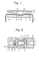
- a package substrate 1 of ceramic has a cavity in the centre portion.
- a gold paste is applied on the bottom surface of the cavity and is heated at a temperature of from 800°C to 950°C to form a gold layer 2.
- a glass paste having a low melting point is applied on the surface of the ceramic substrate 1, except for the cavity, and is pre-baked at a temperature of about 400°C to form a glass layer 3.
- a lead frame which comprises leads 4 and is made of an Fe-Ni-Co alloy (e.g. Kovar) or an Fe-Ni alloy (e.g. 42 Alloy) is set on the glass layer 3, and the ceramic substrate 1 is heated at a temperature of about 450°C to melt the glass layer 3 so that the leads 4 stick to the glass layer 3.
- the chip 5 is put on the gold layer 2 in such a manner that the gold layer 2 is scrubbed with the chip 5.
- the silicon of the integrated-circuit chip 5 is alloyed with the gold of the gold layer 2 to form a eutectic brazing alloy having a low melting point. Therefore, by forming a brazing alloy, the chip can be attached to the package substrate 1.
- a metal terminal chip 6 is attached to the gold layer 2 prior to IC chip attaching step or a wire bonding step to create predetermined electrical connections between the integrated-circuit chip 5 and the leads 4.
- an aluminium micro-wire i.e. a bonding wire
- the aluminium and gold commonly form an intermetallic compound of purple or white plague or plaque when a sealing step of the package is carried out at a temperature of from 400°C to 500°C. This intermetallic compound weakens the bond strength and decreases the electric conductivity, with the result that bond failure may occur.
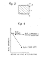
- a metal terminal chip 6 comprising e.g. a metal base 7 being e.g. of an Fe-Ni-Co alloy or an Fe-Ni alloy, an aluminium-silicon (AISi) alloy or aluminium (Al) thin layer 8 formed on the upper surface of the base 7, and a gold-germanium (AuGe) alloy thin layer 9 formed on the lower surface of the base 7, as is illustrated in Figure 3.
- a metal terminal chip is disclosed in Japanese Unexamined Patent Publication JP-A-55-27615.
- the terminal metal chip 6 can be produced by putting an AI or AISi film and an AuGe film on the upper surface and the lower surface of a metal plate, respectively, rolling the films with pressure rollers to form a laminated plate, and punching the plate to form chips.
- the obtained metal chip has a predetermined shape, e.g. a circular or rectangular shape.
- the chip 6 is put on the gold layer 2 so as to bring the AuGe layer 9 into contact with the gold layer 2. Then the gold layer 2 is scrubbed with the chip 6. As a result, the AuGe layer 9 and the gold layer 2 are melted and alloyed.
- the chip 6 sticks to the gold layer 2, i.e. the substrate 1.
- aluminium wires 10 are attached between bonding pads (i.e. contact areas) 11 of the integrated-circuit chip 5 and the terminal areas of the leads 4 by using ultrasonic bonding techniques.
- an aluminium wire 12 is also attached between the AI or AISi layer 8 of the terminal metal chip 6 and a predetermined lead 4A. Therefore, the integrated-circuit chip 5 is grounded via the terminal metal chip 6.
- a ceramic cap 13 ( Figure 1) with a a pre-baked glass layer 14 having a low melting point is put on the glass layer 3 and on the leads 4, and the substrate 1 and the cap 13 are heated at a temperature of from 400°C to 500°C in a furnace. Since the glass layer 14 has a low melting point similar to that of the glass layer 3 the layer 14 is made of the same material as is the layer 3, the glass layer 14 and 13 are melted and are combined into a sealing glass layer. Upon cooling, an hermetically sealed package is produced.
- the metal chips 6 each comprise a metal base 7 having a thickness similarto the thickness of an integrated circuit chip, e.g. about 0.5mm, an upper coating layer 8 having a thickness of from 5 to 15 ⁇ m, e.g. about 10um and a lower coating layer 9 having a thickness of from 25 to 35 pm, e.g. about 30pm.
- the plane shape of the metal chips 6 is a desired form, e.g. a circle having a diameter of 0.9 mm.
- the metal base 7 and the upper coating layer 8 of all of the terminal metal chips are made of a Fe-Ni-Co alloy and an AISi alloy, respectively.
- the lower coating layer 9 is made of an AuSi alloy in a first terminal metal chip, is made of a AuGeSi alloy in a second terminal metal chip, and is made of a AuGe alloy in a third terminal metal chip.
- the first and second terminal metal chips are embodiments of the present invention, and the third terminal metal chip is a conventional chip.
- Each of the three types ofterminal metal chips is attached to the gold layer 2 formed on the package substrate 1 ( Figures 1 and 2) by scrubbing while the substrate 1 is being heated at a temperature of 430°C and after the integrated-circuit chip 5 of silicon is attached to the gold layer 2. After cooling, all of the package substrates, along with the terminal metal chips, are heated at a temperature of 450°C. This heat treatment is carried out under the same conditions as those in the case of glass sealing.
- the bond strength of'the terminal metal chips is measured by applying a force to each of the terminal metal chips in a horizontal direction in an attempt to remove the chip both before and after heating.
- the measurement results are shown in Figure 4.
- the bond strength of the first and second terminal metal chips having AuSi and AuGeSi lower coating layers, respectively is not decreased substantially, but the bond strength of the third terminal metal chip having a AuGe layer is remarkably decreased to about one third the initial value.
- the lower coating layer 9 is made of a AuSi type of alloy in accordance with the present invention instead of a AuGe alloy, whereby a decrease in the bond strength of the terminal metal chip can be prevented.
- semiconductor devices so produced have an improved reliability in comparison with a conventional semiconductor device.
Landscapes
- Lead Frames For Integrated Circuits (AREA)
- Die Bonding (AREA)
- Wire Bonding (AREA)
Claims (5)
Applications Claiming Priority (2)
| Application Number | Priority Date | Filing Date | Title |
|---|---|---|---|
| JP57050734A JPS58169942A (ja) | 1982-03-29 | 1982-03-29 | 半導体装置 |
| JP50734/82 | 1982-03-29 |
Publications (3)
| Publication Number | Publication Date |
|---|---|
| EP0090566A2 EP0090566A2 (fr) | 1983-10-05 |
| EP0090566A3 EP0090566A3 (en) | 1985-10-30 |
| EP0090566B1 true EP0090566B1 (fr) | 1989-01-25 |
Family
ID=12867075
Family Applications (1)
| Application Number | Title | Priority Date | Filing Date |
|---|---|---|---|
| EP83301536A Expired EP0090566B1 (fr) | 1982-03-29 | 1983-03-18 | Empaquetage pour dispositif semi-conducteur |
Country Status (5)
| Country | Link |
|---|---|
| US (1) | US4558346A (fr) |
| EP (1) | EP0090566B1 (fr) |
| JP (1) | JPS58169942A (fr) |
| DE (1) | DE3379090D1 (fr) |
| IE (1) | IE54534B1 (fr) |
Families Citing this family (12)
| Publication number | Priority date | Publication date | Assignee | Title |
|---|---|---|---|---|
| US4570337A (en) * | 1982-04-19 | 1986-02-18 | Olin Corporation | Method of assembling a chip carrier |
| EP0139029A1 (fr) * | 1983-10-19 | 1985-05-02 | Olin Corporation | Empaquetage pour semi-conducteur |
| US4837928A (en) * | 1986-10-17 | 1989-06-13 | Cominco Ltd. | Method of producing a jumper chip for semiconductor devices |
| JPH06244231A (ja) * | 1993-02-01 | 1994-09-02 | Motorola Inc | 気密半導体デバイスおよびその製造方法 |
| JP2938344B2 (ja) * | 1994-05-15 | 1999-08-23 | 株式会社東芝 | 半導体装置 |
| US5508556A (en) * | 1994-09-02 | 1996-04-16 | Motorola, Inc. | Leaded semiconductor device having accessible power supply pad terminals |
| JPH11305205A (ja) * | 1998-04-22 | 1999-11-05 | Hitachi Ltd | 液晶表示装置 |
| US6062461A (en) * | 1998-06-03 | 2000-05-16 | Delphi Technologies, Inc. | Process for bonding micromachined wafers using solder |
| US6564449B1 (en) * | 2000-11-07 | 2003-05-20 | Advanced Semiconductor Engineering, Inc. | Method of making wire connection in semiconductor device |
| KR100706516B1 (ko) | 2001-02-06 | 2007-04-11 | 앰코 테크놀로지 코리아 주식회사 | 반도체 패키지 |
| US20130167482A1 (en) * | 2011-09-08 | 2013-07-04 | Advanced Numicro Systems, Inc. | Vacuum sealing process of a mems package |
| US10014189B2 (en) * | 2015-06-02 | 2018-07-03 | Ngk Spark Plug Co., Ltd. | Ceramic package with brazing material near seal member |
Family Cites Families (11)
| Publication number | Priority date | Publication date | Assignee | Title |
|---|---|---|---|---|
| US3497774A (en) * | 1967-06-07 | 1970-02-24 | Beckman Instruments Inc | Electrical circuit module and method of manufacture |
| US3585711A (en) * | 1968-09-06 | 1971-06-22 | Us Navy | Gold-silicon bonding process |
| JPS5840370B2 (ja) * | 1974-09-03 | 1983-09-05 | 日本電気株式会社 | ゾウフクカイロ |
| JPS598358Y2 (ja) * | 1978-02-08 | 1984-03-15 | 京セラ株式会社 | 半導体素子パツケ−ジ |
| JPS5910584B2 (ja) * | 1978-08-17 | 1984-03-09 | 住友金属鉱山株式会社 | Icパツケ−ジ用クラツド材 |
| JPS55153341A (en) * | 1979-05-17 | 1980-11-29 | Toshiba Corp | Semiconductor device |
| JPS56105660A (en) * | 1980-01-28 | 1981-08-22 | Nec Corp | Semiconductor device |
| EP0039507A1 (fr) * | 1980-05-05 | 1981-11-11 | LeaRonal, Inc. | Procédé pour la mise en boîtier d'un semiconducteur, et structure de raccordement pour des éléments semiconducteurs |
| JPS5758340A (en) * | 1980-09-24 | 1982-04-08 | Nec Corp | Semiconductor device |
| JPS5854644A (ja) * | 1981-09-28 | 1983-03-31 | Nec Corp | ボンデイング用樹脂基板 |
| US4447857A (en) * | 1981-12-09 | 1984-05-08 | International Business Machines Corporation | Substrate with multiple type connections |
-
1982
- 1982-03-29 JP JP57050734A patent/JPS58169942A/ja active Pending
-
1983
- 1983-03-18 DE DE8383301536T patent/DE3379090D1/de not_active Expired
- 1983-03-18 EP EP83301536A patent/EP0090566B1/fr not_active Expired
- 1983-03-23 US US06/477,934 patent/US4558346A/en not_active Expired - Lifetime
- 1983-03-29 IE IE707/83A patent/IE54534B1/en not_active IP Right Cessation
Also Published As
| Publication number | Publication date |
|---|---|
| JPS58169942A (ja) | 1983-10-06 |
| IE830707L (en) | 1983-09-29 |
| IE54534B1 (en) | 1989-11-08 |
| EP0090566A2 (fr) | 1983-10-05 |
| EP0090566A3 (en) | 1985-10-30 |
| US4558346A (en) | 1985-12-10 |
| DE3379090D1 (en) | 1989-03-02 |
Similar Documents
| Publication | Publication Date | Title |
|---|---|---|
| US7008824B2 (en) | Method of fabricating mounted multiple semiconductor dies in a package | |
| US6297547B1 (en) | Mounting multiple semiconductor dies in a package | |
| JPH08264697A (ja) | 半導体リードフレーム構造およびその製造方法 | |
| JPH08116016A (ja) | リードフレーム及び半導体装置 | |
| EP0090566B1 (fr) | Empaquetage pour dispositif semi-conducteur | |
| US5378657A (en) | Method for making an aluminum clad leadframe and a semiconductor device employing the same | |
| JPH0350758A (ja) | 樹脂封止型半導体装置 | |
| JPS60167454A (ja) | 半導体装置 | |
| US5055911A (en) | Semiconductor device package utilizing a solder flow prevention wall | |
| US4745036A (en) | Jumper chip for semiconductor devices | |
| CA1201211A (fr) | Enveloppe hermetique de semiconducteur | |
| US4837928A (en) | Method of producing a jumper chip for semiconductor devices | |
| JPH0567069B2 (fr) | ||
| JPS634350B2 (fr) | ||
| JP2572092Y2 (ja) | 半導体素子パッケージ | |
| JPH0525182B2 (fr) | ||
| JPH03108361A (ja) | 半導体集積回路装置 | |
| JPS62183133A (ja) | 半導体装置 | |
| JPS60165742A (ja) | 半導体装置 | |
| JPS6236287Y2 (fr) | ||
| JPS63107126A (ja) | 半導体装置 | |
| JPS6025900Y2 (ja) | 半導体装置 | |
| JPS613438A (ja) | プラスチツク封止型ic | |
| JPH02244658A (ja) | 半導体装置 | |
| JPS6155778B2 (fr) |
Legal Events
| Date | Code | Title | Description |
|---|---|---|---|
| PUAI | Public reference made under article 153(3) epc to a published international application that has entered the european phase |
Free format text: ORIGINAL CODE: 0009012 |
|
| AK | Designated contracting states |
Designated state(s): DE FR GB |
|
| PUAL | Search report despatched |
Free format text: ORIGINAL CODE: 0009013 |
|
| AK | Designated contracting states |
Designated state(s): DE FR GB |
|
| 17P | Request for examination filed |
Effective date: 19860218 |
|
| 17Q | First examination report despatched |
Effective date: 19870507 |
|
| GRAA | (expected) grant |
Free format text: ORIGINAL CODE: 0009210 |
|
| AK | Designated contracting states |
Kind code of ref document: B1 Designated state(s): DE FR GB |
|
| REF | Corresponds to: |
Ref document number: 3379090 Country of ref document: DE Date of ref document: 19890302 |
|
| ET | Fr: translation filed | ||
| PLBE | No opposition filed within time limit |
Free format text: ORIGINAL CODE: 0009261 |
|
| STAA | Information on the status of an ep patent application or granted ep patent |
Free format text: STATUS: NO OPPOSITION FILED WITHIN TIME LIMIT |
|
| 26N | No opposition filed | ||
| PGFP | Annual fee paid to national office [announced via postgrant information from national office to epo] |
Ref country code: FR Payment date: 19911231 Year of fee payment: 10 |
|
| PGFP | Annual fee paid to national office [announced via postgrant information from national office to epo] |
Ref country code: GB Payment date: 19920311 Year of fee payment: 10 |
|
| PGFP | Annual fee paid to national office [announced via postgrant information from national office to epo] |
Ref country code: DE Payment date: 19920522 Year of fee payment: 10 |
|
| PG25 | Lapsed in a contracting state [announced via postgrant information from national office to epo] |
Ref country code: GB Effective date: 19930318 |
|
| GBPC | Gb: european patent ceased through non-payment of renewal fee |
Effective date: 19930318 |
|
| PG25 | Lapsed in a contracting state [announced via postgrant information from national office to epo] |
Ref country code: FR Effective date: 19931130 |
|
| PG25 | Lapsed in a contracting state [announced via postgrant information from national office to epo] |
Ref country code: DE Effective date: 19931201 |
|
| REG | Reference to a national code |
Ref country code: FR Ref legal event code: ST |