EP0092150A2 - Sich verformender elektrischer Verbinder - Google Patents
Sich verformender elektrischer Verbinder Download PDFInfo
- Publication number
- EP0092150A2 EP0092150A2 EP83103543A EP83103543A EP0092150A2 EP 0092150 A2 EP0092150 A2 EP 0092150A2 EP 83103543 A EP83103543 A EP 83103543A EP 83103543 A EP83103543 A EP 83103543A EP 0092150 A2 EP0092150 A2 EP 0092150A2
- Authority
- EP
- European Patent Office
- Prior art keywords
- pin
- groove
- connector
- hole
- grooves
- Prior art date
- Legal status (The legal status is an assumption and is not a legal conclusion. Google has not performed a legal analysis and makes no representation as to the accuracy of the status listed.)
- Withdrawn
Links
Images
Classifications
-
- H—ELECTRICITY
- H01—ELECTRIC ELEMENTS
- H01R—ELECTRICALLY-CONDUCTIVE CONNECTIONS; STRUCTURAL ASSOCIATIONS OF A PLURALITY OF MUTUALLY-INSULATED ELECTRICAL CONNECTING ELEMENTS; COUPLING DEVICES; CURRENT COLLECTORS
- H01R12/00—Structural associations of a plurality of mutually-insulated electrical connecting elements, specially adapted for printed circuits, e.g. printed circuit boards [PCB], flat or ribbon cables, or like generally planar structures, e.g. terminal strips, terminal blocks; Coupling devices specially adapted for printed circuits, flat or ribbon cables, or like generally planar structures; Terminals specially adapted for contact with, or insertion into, printed circuits, flat or ribbon cables, or like generally planar structures
- H01R12/50—Fixed connections
- H01R12/51—Fixed connections for rigid printed circuits or like structures
- H01R12/55—Fixed connections for rigid printed circuits or like structures characterised by the terminals
- H01R12/58—Fixed connections for rigid printed circuits or like structures characterised by the terminals terminals for insertion into holes
- H01R12/585—Terminals having a press fit or a compliant portion and a shank passing through a hole in the printed circuit board
Definitions
- This invention relates generally to the joining of electrical contacts or connectors to circuit boards and, more particularly, concerns the construction of such contacts or connection to provide compliance or self-adjustment giving intimate contact with plating at a hole through the board, and enhancing reliability.
- the "backplane” still employs a plurality of posts, emanating from the back sides of the edge card connectors. These posts are wired by wire wrapping methods to program the computer, during manufacture. Program changes, and new programs are made by transistor switching. Further development of the "backplane” embodied the introduction of large, thicker printed wiring boards, with interconnecting circuits, to eliminate up to about 75% of wire wrap connections.
- One known connector provides a post that adjusts itself to various hole sizes; however, it is violently overstressed when pressed into the plated hole, with reliability being about 98% good. The remaining 21% are good until thermal conditions create stress relaxation in the contact material and intermittent contact results (intermittency is the most troublesome fault).
- Another known compliant device operates like a spring "roll pin". This is effective but is costly to produce, and cannot be produced in close proximity to adjacent contacts, such as raw material is used to produce this device. Other known devices employ through slots in the center of the metal of the compliant section. Extension testing shows that this approach is even less reliable than the first one, unless one starts, to again limit the hole size. Accordingly, there is need for a highly reliable compliant pin, making good contact with plating at all temperatures.
- the connector is adapted to be pressed endwise into a hole in a circuit board, and comprises:
- the flexure is typically centrally located between crests defined by the convexly curved opposite outer sides, and in such manner that a Z-shaped cross section is formed, with the flexure assuming an S-shaped flexed configuration, these two Z-shaped and S-shaped configurations contributing to maximum relative displacement of the convex outer surfaces, in use.
- these S-shaped and Z-shaped configurations combine to define a spring that will return to its stamped shape on removal of compressive forces. When deflected inwardly, by such action, energy is stored in the spring members, developing outwardly opposing forces exerted by the convex outer surfaces against the walls of the hole.
- the confining hole is plated in a backplane circuit board.
- Such holes typically have an electroplated layer of copper and covering this a layer of electroplated pin or tin/lead alloy.
- the spring action of the contact section will create outwardly directed forces such that intimate electrical contact is made, over a wide area, while the pin is held firmly in its inserted location, such that subsequent operations--wire wrapping--1ogic board interconnection, etc., do not dislodge the contact or disturb the intimate electrical connection.
- the configuration of the contact enables its manufacture in a continuous strip, with very small spacing between adjacent contacts.
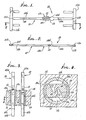
- the contact or connector 10 is shown to include an axially elongated flat pin 12.
- the latter includes a first section 12a, a wire wrap post section 12b, and intermediate sections 12c and 12d joining the sections 12a and 12b.
- the latter are shown in Fig. 1 to have the same width, which is less than the width of section 12c.
- During stamped formation of the pin its opposite ends may be joined to elongated strips lla and llb, as at break-off narrowed connections 110 and 111.
- Step shoulder 13 formed at the junction of sections 12c and 12d is adapted to engage the printed circuit backplane board 14, or the plating 15a thereon, upon insertion of the connector into the board, thereby to limit such insertion.
- Fig. 3 shows two such connectors 10 inserted through openings or holes 16 the bores of which are plated at 15b with electrically conductive material.
- the pin section 12c has opposite outer surfaces to forcibly grip the structure (as for example plating 15b) at the boundary of the hole as the pin is inserted into the hole.
- the pin section 12c has convex opposite outer surfaces 19 and 20 with curvature generally matching that of the circular bore 18.
- Such surfaces forcibly and frictionally grip the bore 18 of plating 15b upon insertion of the section 12c into the opening 16, and as will be explained, the cross section 12c' yieldably reduces in lateral length so that the section end surfaces move from broken line positions 19a and 20a to the full line positions 19 and 20 indicated in Fig. 4. Note that the surfaces 19 and 20 distribute their grip loading over a large contact area, for assurance of good electrical contact and maintenance of the integrity of the bore wall 18, without scoring same.
- the pin has at least one elongated groove sunk in the side thereof, the groove extending axially of the pin and configured to locally weaken the pin so that at least one flexure is formed by the pin to extend axially thereof adjacent the groove and along the groove length.
- the flexure is adapted to yieldably flex in response to insertion of the pin into the hole and in response to progressive gripping of the hole forming structure by the pin edges, thereby to reduce the cross sectional area of groove in response to insertion of the pin into the hole.
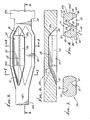
- each groove 21 and 22 are sunk in opposite outer sides 23 and 24 respectively of section 12c, giving the cross section a Z-shape.
- Each groove has opposite side walls 25 and 26 forming generally V-shaped groove cross sections along major length extent of the groove, and in planes normal to the pin axis 28. Also, the bottoms of the grooves are concavely rounded as at 29.
- the depth of each groove is such as to accomodate relative movement of the walls 25 and 26 toward one another in response to insertion of the pin into the hole. Note in Fig. 4 that the full depth of each groove is greater that 1/2 the thickness of the section 12c between sides 23 and 24 but less than 3/4 that thickness for best results.
- the flexure formed at 40 between the two grooves defines a plane 41 that extends at angle 0 (. relative to each side 23 and 24. That angle is between 45° and 75°, in unflexed condition of the flexure whereby maximum flexing and relative displacement of surfaces 19 and 20 are achieved.
- the flexure In flexed condition, as in Fig. 4, the flexure has S-shape, walls 25 are concave, and walls 26 are concave; whereas in Fig. 8 walls 25 and 26 are generally flat.
- the center of the flexure, i.e., at 28, lies midway between crests 19a' and 20a' of surfaces 19 and 20.
- Figs. 5 and 7 show that the groove depth progressively increases along the generally triangular groove bottom wall 31 between the flat outer surface 32 and the full groove depth 29, at one end of the groove; likewise, at the opposite end of the groove, the depth progressively increases along the generally triangular groove bottom wall 33 between the transverse plane of shoulder 13 and the full groove depth.
- Walls 31 and 33 concavely merge at 31a and 33a with groove walls 25 and 26, for best results.
- Ease of entry to prevent sudden disruption of a hole surface is thereby achieved in two ways with this design: the profile shape of the compliant section prevents gouging of the bore and distributes compression loading for good electrical contact, and the leading ends of the grooves making the bellows shape, are angled to allow deflection to occur progressively.
- too obtuse an angle between groove walls 25 and 26 would overstress the metal during manufacture, and could cause fracture of the metal, while too sharp an angle would'fall to develop forces that act throughout the length of the hole.
- the spring action of the present design provides sufficient developed force to allow for, and compensate for, some loss of strength that occurs in any spring. Loss of strength is caused by heat and time, such losses being approximately the same for low heat/long time and for high heat/short time. Computers normally get hot, but are cooled by mechanical means to approximately to 50°C. At this temperature, 10 to 15 percent of a spring force is lost after 1,000 hours. Therefore, one must provide an initial surplus of force so that there is still an adequate residual force over the lifetime of the product. Such stress relaxation is not linear, and is to some degree self limiting. The force/area ratio (i.e. pressure) involved with this design is such that loss of 15% of the force gives only a very small drop in pressure.
Landscapes
- Multi-Conductor Connections (AREA)
- Coupling Device And Connection With Printed Circuit (AREA)
Applications Claiming Priority (2)
| Application Number | Priority Date | Filing Date | Title |
|---|---|---|---|
| US06/369,170 US4475780A (en) | 1982-04-16 | 1982-04-16 | Compliant electrical connector |
| US369170 | 2003-02-18 |
Publications (2)
| Publication Number | Publication Date |
|---|---|
| EP0092150A2 true EP0092150A2 (de) | 1983-10-26 |
| EP0092150A3 EP0092150A3 (de) | 1986-12-03 |
Family
ID=23454376
Family Applications (1)
| Application Number | Title | Priority Date | Filing Date |
|---|---|---|---|
| EP83103543A Withdrawn EP0092150A3 (de) | 1982-04-16 | 1983-04-13 | Sich verformender elektrischer Verbinder |
Country Status (3)
| Country | Link |
|---|---|
| US (1) | US4475780A (de) |
| EP (1) | EP0092150A3 (de) |
| JP (1) | JPS58189970A (de) |
Cited By (12)
| Publication number | Priority date | Publication date | Assignee | Title |
|---|---|---|---|---|
| DE3326598A1 (de) * | 1983-07-23 | 1985-02-07 | EPT Elektronische Präzisionsteile GmbH & Co, 8922 Peiting | Steckerstift fuer leiterplatten von elektronischen bauteilen sowie isolierkoerper zur aufnahme solcher steckerstifte |
| EP0148792A3 (en) * | 1984-01-12 | 1986-10-08 | H & V Services | Compliant pin |
| EP0124767A3 (de) * | 1983-04-07 | 1986-12-03 | BMC Industries, Inc. | Sich verformender Stift |
| US4691979A (en) * | 1983-08-04 | 1987-09-08 | Manda R & D | Compliant press-fit electrical contact |
| EP0263630A1 (de) * | 1986-10-06 | 1988-04-13 | Amp Incorporated | Elektrischer Anschluss für gedruckte Leiterplatte und Verfahren zu seiner Herstellung |
| EP0132704A3 (de) * | 1983-07-23 | 1988-04-20 | Guglhör, Magdalena | Kontaktstift für elektronische Bauteile, insbesondere Leiterplatten |
| EP0331293A3 (en) * | 1988-02-29 | 1990-06-06 | Molex Incorporated | Electrical terminal pin with compliant portion |
| EP0468460A1 (de) * | 1990-07-26 | 1992-01-29 | Hirose Electric Co., Ltd. | Elektrischer Anschlusskontakt und Herstellungsverfahren |
| US5511996A (en) * | 1994-11-14 | 1996-04-30 | A.W. Industries, Inc. | Connector contact and method |
| US5944563A (en) * | 1994-08-30 | 1999-08-31 | Nec Corporation | Press-in terminal for a connector |
| EP1372220A1 (de) * | 2002-06-12 | 2003-12-17 | Sumitomo Wiring Systems, Ltd. | Anschlusskontakt für Leiterplatte |
| WO2019067347A1 (en) * | 2017-09-28 | 2019-04-04 | Interplex Industries, Inc. | CONTACT PROVIDED WITH A PRESSURE ADJUSTING FASTENING ELEMENT |
Families Citing this family (18)
| Publication number | Priority date | Publication date | Assignee | Title |
|---|---|---|---|---|
| JPS6041783A (ja) * | 1983-04-07 | 1985-03-05 | ビ−エムシ−・インダストリ−ズ・インコ−ポレ−テツド | 適応ピン |
| US4586778A (en) * | 1983-08-25 | 1986-05-06 | Bmc Industries, Inc. | Compliant pin |
| JPS61138475A (ja) * | 1984-12-10 | 1986-06-25 | 日本電気株式会社 | 電気接触ピン |
| US4793817A (en) * | 1985-02-27 | 1988-12-27 | Karl Neumayer, Erzeugung Und Vertreib Von Kabeln, Drahten Isolierten Leitungen Und Elektromaterial Gesellschaft Mit Beschrankter Haftung | Contact pin |
| JPS625575A (ja) * | 1985-07-02 | 1987-01-12 | ヒロセ電機株式会社 | 電気接触ピン |
| US4681392A (en) * | 1986-04-21 | 1987-07-21 | Bead Chain Manufacturing Company | Swaged compliant connector pins for printed circuit boards |
| US4780958A (en) * | 1986-10-06 | 1988-11-01 | Amp Incorporated | Method of making an electrical terminal for a printed circuit board |
| US4746301A (en) * | 1986-10-29 | 1988-05-24 | Key Edward H | S-shaped compliant pin |
| US4831728A (en) * | 1987-06-05 | 1989-05-23 | Northern Telecom Limited | Method of making circuit board pin |
| US4878861A (en) * | 1988-11-01 | 1989-11-07 | Elfab Corporation | Compliant electrical connector pin |
| US4906198A (en) * | 1988-12-12 | 1990-03-06 | International Business Machines Corporation | Circuit board assembly and contact pin for use therein |
| US4969259A (en) * | 1988-12-14 | 1990-11-13 | International Business Machines Corporation | Pin with tubular elliptical compliant portion and method for affixing to mating receptacle |
| DE4002486A1 (de) * | 1990-01-29 | 1991-08-08 | Polytronic Kunststoff Elektro | Kontaktelement mit einer einpresszone |
| US5573431A (en) * | 1995-03-13 | 1996-11-12 | Wurster; Woody | Solderless contact in board |
| DE102004006533A1 (de) * | 2004-02-11 | 2005-09-01 | Conti Temic Microelectronic Gmbh | Elektrisch leitfähiger Kontaktstift zum Einpressen in eine Öffnung einer Leiterplatte sowie elektrische Baugruppe mit einem solchen Kontaktstift |
| JP2008053091A (ja) * | 2006-08-25 | 2008-03-06 | Honda Tsushin Kogyo Co Ltd | プレスフィットコンタクト |
| JP2011077022A (ja) * | 2009-09-03 | 2011-04-14 | Sumitomo Wiring Syst Ltd | 基板用端子 |
| CN116632569A (zh) * | 2023-05-15 | 2023-08-22 | 安费诺(常州)高端连接器有限公司 | 一种垂直插入顺应针、电子组件及其使用方法 |
Family Cites Families (11)
| Publication number | Priority date | Publication date | Assignee | Title |
|---|---|---|---|---|
| US3444617A (en) * | 1965-11-05 | 1969-05-20 | Ibm | Self-positioning and collapsing standoff for a printed circuit connection and method of achieving the same |
| US3566343A (en) * | 1968-08-26 | 1971-02-23 | Amp Inc | Electrical connectors for terminating leads of micro-modular components or the like |
| NL149675B (nl) * | 1972-05-10 | 1976-05-17 | Berg Electronics B V | Ketenplaatpen. |
| US3824554A (en) * | 1972-08-28 | 1974-07-16 | G Shoholm | Spring-type press-fit |
| GB1470007A (en) * | 1973-08-01 | 1977-04-14 | Amp Inc | Electrical contact pin |
| US3907400A (en) * | 1973-11-21 | 1975-09-23 | Du Pont | Contact post |
| US3975078A (en) * | 1974-04-15 | 1976-08-17 | Elfab Corporation | Folded electrical contact |
| IT1046588B (it) * | 1974-06-21 | 1980-07-31 | Amf Inc | Spinotto di contatto elettrico |
| US4017143A (en) * | 1975-12-16 | 1977-04-12 | Litton Systems, Inc. | Solderless electrical contact |
| US4274699A (en) * | 1978-04-27 | 1981-06-23 | E. I. Du Pont De Nemours And Company | Press fit terminal with spring arm contact for edgecard connector |
| US4223970A (en) * | 1979-02-26 | 1980-09-23 | Electronics Stamping Corporation | Compliant backplane electrical connector |
-
1982
- 1982-04-16 US US06/369,170 patent/US4475780A/en not_active Expired - Fee Related
-
1983
- 1983-04-13 EP EP83103543A patent/EP0092150A3/de not_active Withdrawn
- 1983-04-15 JP JP58066823A patent/JPS58189970A/ja active Pending
Cited By (14)
| Publication number | Priority date | Publication date | Assignee | Title |
|---|---|---|---|---|
| EP0124767A3 (de) * | 1983-04-07 | 1986-12-03 | BMC Industries, Inc. | Sich verformender Stift |
| DE3326598A1 (de) * | 1983-07-23 | 1985-02-07 | EPT Elektronische Präzisionsteile GmbH & Co, 8922 Peiting | Steckerstift fuer leiterplatten von elektronischen bauteilen sowie isolierkoerper zur aufnahme solcher steckerstifte |
| EP0132704A3 (de) * | 1983-07-23 | 1988-04-20 | Guglhör, Magdalena | Kontaktstift für elektronische Bauteile, insbesondere Leiterplatten |
| US4691979A (en) * | 1983-08-04 | 1987-09-08 | Manda R & D | Compliant press-fit electrical contact |
| EP0148792A3 (en) * | 1984-01-12 | 1986-10-08 | H & V Services | Compliant pin |
| EP0263630A1 (de) * | 1986-10-06 | 1988-04-13 | Amp Incorporated | Elektrischer Anschluss für gedruckte Leiterplatte und Verfahren zu seiner Herstellung |
| EP0331293A3 (en) * | 1988-02-29 | 1990-06-06 | Molex Incorporated | Electrical terminal pin with compliant portion |
| EP0468460A1 (de) * | 1990-07-26 | 1992-01-29 | Hirose Electric Co., Ltd. | Elektrischer Anschlusskontakt und Herstellungsverfahren |
| US5944563A (en) * | 1994-08-30 | 1999-08-31 | Nec Corporation | Press-in terminal for a connector |
| US5511996A (en) * | 1994-11-14 | 1996-04-30 | A.W. Industries, Inc. | Connector contact and method |
| EP1372220A1 (de) * | 2002-06-12 | 2003-12-17 | Sumitomo Wiring Systems, Ltd. | Anschlusskontakt für Leiterplatte |
| US6875032B2 (en) | 2002-06-12 | 2005-04-05 | Sumitomo Wiring Systems, Ltd. | Circuit board terminal |
| WO2019067347A1 (en) * | 2017-09-28 | 2019-04-04 | Interplex Industries, Inc. | CONTACT PROVIDED WITH A PRESSURE ADJUSTING FASTENING ELEMENT |
| US11095057B2 (en) | 2017-09-28 | 2021-08-17 | Interplex Industries, Inc. | Contact with a press-fit fastener |
Also Published As
| Publication number | Publication date |
|---|---|
| JPS58189970A (ja) | 1983-11-05 |
| US4475780A (en) | 1984-10-09 |
| EP0092150A3 (de) | 1986-12-03 |
Similar Documents
| Publication | Publication Date | Title |
|---|---|---|
| US4475780A (en) | Compliant electrical connector | |
| US4223970A (en) | Compliant backplane electrical connector | |
| US4647126A (en) | Compliant lead clip | |
| US7309242B2 (en) | Power connector | |
| US4828503A (en) | Printed circuit board connector | |
| US6042389A (en) | Low profile connector | |
| US6135781A (en) | Electrical interconnection system and device | |
| US6358068B1 (en) | Stress resistant connector and method for reducing stress in housing thereof | |
| US3530422A (en) | Connector and method for attaching same to printed circuit board | |
| US4217024A (en) | Dip socket having preloading and antiwicking features | |
| US20110076897A1 (en) | High Density Connector and Method of Manufacture | |
| WO1998002942A9 (en) | Electrical interconnection system and device | |
| US20020142651A1 (en) | Electrical connector | |
| US4756696A (en) | Solder joint inspection feature for surface mount connectors | |
| CN101682136A (zh) | 板卡边缘电缆连接器 | |
| USRE32212E (en) | Compliant backplane electrical connector | |
| US3414865A (en) | Electrical connectors | |
| US6834791B2 (en) | Solder-bearing components and method of retaining a solder mass therein | |
| US5971793A (en) | Multi-conductor cable connector | |
| US4793060A (en) | Manufacture of low profile clip connector | |
| EP1770828B1 (de) | Elektrische Anschlussblöcke mit Signal- und Leistungseigenschaften | |
| JPH01268086A (ja) | フレキシブルプリント基板 | |
| HK1019966B (en) | Electrical interconnection system and device | |
| HK1000404A1 (en) | Low insertion force connector and electrical contact therefor | |
| HK1022383B (en) | Low profile connector |
Legal Events
| Date | Code | Title | Description |
|---|---|---|---|
| PUAI | Public reference made under article 153(3) epc to a published international application that has entered the european phase |
Free format text: ORIGINAL CODE: 0009012 |
|
| AK | Designated contracting states |
Designated state(s): AT BE CH DE FR GB IT LI LU NL SE |
|
| PUAL | Search report despatched |
Free format text: ORIGINAL CODE: 0009013 |
|
| AK | Designated contracting states |
Kind code of ref document: A3 Designated state(s): AT BE CH DE FR GB IT LI LU NL SE |
|
| 17P | Request for examination filed |
Effective date: 19870508 |
|
| 17Q | First examination report despatched |
Effective date: 19871214 |
|
| STAA | Information on the status of an ep patent application or granted ep patent |
Free format text: STATUS: THE APPLICATION IS DEEMED TO BE WITHDRAWN |
|
| 18D | Application deemed to be withdrawn |
Effective date: 19880426 |
|
| RIN1 | Information on inventor provided before grant (corrected) |
Inventor name: WALTER, LEO Inventor name: GREUL, W. HELMUT |