EP0092409A1 - Procédé de fabrication d'un monocristal d'arséniure de gallium dopé au bore - Google Patents
Procédé de fabrication d'un monocristal d'arséniure de gallium dopé au bore Download PDFInfo
- Publication number
- EP0092409A1 EP0092409A1 EP83302165A EP83302165A EP0092409A1 EP 0092409 A1 EP0092409 A1 EP 0092409A1 EP 83302165 A EP83302165 A EP 83302165A EP 83302165 A EP83302165 A EP 83302165A EP 0092409 A1 EP0092409 A1 EP 0092409A1
- Authority
- EP
- European Patent Office
- Prior art keywords
- boron
- gaas
- crystals
- mixture
- single crystals
- Prior art date
- Legal status (The legal status is an assumption and is not a legal conclusion. Google has not performed a legal analysis and makes no representation as to the accuracy of the status listed.)
- Granted
Links
Images

Classifications
-
- C—CHEMISTRY; METALLURGY
- C30—CRYSTAL GROWTH
- C30B—SINGLE-CRYSTAL GROWTH; UNIDIRECTIONAL SOLIDIFICATION OF EUTECTIC MATERIAL OR UNIDIRECTIONAL DEMIXING OF EUTECTOID MATERIAL; REFINING BY ZONE-MELTING OF MATERIAL; PRODUCTION OF A HOMOGENEOUS POLYCRYSTALLINE MATERIAL WITH DEFINED STRUCTURE; SINGLE CRYSTALS OR HOMOGENEOUS POLYCRYSTALLINE MATERIAL WITH DEFINED STRUCTURE; AFTER-TREATMENT OF SINGLE CRYSTALS OR A HOMOGENEOUS POLYCRYSTALLINE MATERIAL WITH DEFINED STRUCTURE; APPARATUS THEREFOR
- C30B27/00—Single-crystal growth under a protective fluid
- C30B27/02—Single-crystal growth under a protective fluid by pulling from a melt
-
- C—CHEMISTRY; METALLURGY
- C30—CRYSTAL GROWTH
- C30B—SINGLE-CRYSTAL GROWTH; UNIDIRECTIONAL SOLIDIFICATION OF EUTECTIC MATERIAL OR UNIDIRECTIONAL DEMIXING OF EUTECTOID MATERIAL; REFINING BY ZONE-MELTING OF MATERIAL; PRODUCTION OF A HOMOGENEOUS POLYCRYSTALLINE MATERIAL WITH DEFINED STRUCTURE; SINGLE CRYSTALS OR HOMOGENEOUS POLYCRYSTALLINE MATERIAL WITH DEFINED STRUCTURE; AFTER-TREATMENT OF SINGLE CRYSTALS OR A HOMOGENEOUS POLYCRYSTALLINE MATERIAL WITH DEFINED STRUCTURE; APPARATUS THEREFOR
- C30B29/00—Single crystals or homogeneous polycrystalline material with defined structure characterised by the material or by their shape
- C30B29/10—Inorganic compounds or compositions
- C30B29/40—AIIIBV compounds wherein A is B, Al, Ga, In or Tl and B is N, P, As, Sb or Bi
- C30B29/42—Gallium arsenide
Definitions
- This invention relates to a process for manufacturing boron-doped GaAs single crystals of low dislocation density which are suitable for preparing a stable semi-insulating substrate.
- GaAs gallium arsenide
- a semi-insulating substance is generally meant as a substance having a resistivity between 10 and 10 9 ⁇ cm.
- the single crystals of GaAs of high purity produced by the LEC method are commercially available in the form of ⁇ 100> wafers having a diameter of two or three inches.
- the gallium arsenide produced by the LEC method has, however, a dislocation density of 10 4 to 10 5 cm -2 which is 10 to 100 times higher than that of GaAs obtained by the HB (Horizontal Bridgman) method. Since the effects which dislocation may have on the yield and stability of IC devices employing semi-insulating GaAs have been recently clarified, it is essential to use GaAs crystals of low dislocation density in order to obtain devices of higher stability.
- the electrical property with dislocation is different from that without dislocations, because the impurities are gettering at neighbor of dislocations.
- the bond energy between B and As is 72.9 kcal/mol and higher than that between Ga and As in the matrix (47.7 kcal/mol), and which ensures greater resistance to dislocation, since boron atoms resist dislocation, and they are considered to be electrically neutral in GaAs.
- boron, gallium and arsenic are used as the starting materials, and the LEC method is repeated. If the pulled crystal is a poly-crystal, the LEC method repeats further.
- This invention enables one to produce boron-doped GaAs single crystals containing a large quantity of boron in a relatively short time (for example, about one day) with accurate control of boron content.
- the boron content in the crystal is higher than 10 17 cm -3 . According to this invention, therefore, it is easy to produce semi-insulating GaAs single crystals of low dislocation density less than about 10 4 cm -2 .
- a mixture of boron, gallium and arsenic is coated with a liquid encapsulant (B 2 O 3 ), and melted.
- the boron content in the mixture of B, Ga and As is higher than 28.3 wt. ppm.
- the mole-fraction of As is higher than that of Ga, for example, 1.01-1.05 times that of Ga.
- boron-doped GaAs crystals are pulled up from the mixture melts by the LEC method.
- the seed end is removed from the crystal, and a small piece is formed from the grown crystal.
- the size of a piece is cubes of about 1 cm.
- the small piece is remelted in the presence of the liquid encapsulant B 2 0 3 , with boron if required, and boron-doped GaAs single crystals are pulled up by the LEC method.
- the additional B content is less than 50 wt. ppm. It is necessary to use B, Ga, As and B 2 O 3 which are uf the highest possible purity and a crucible which is substantially free from any impurities, for example, artificial boron nitride. Except B, the impurity concentrations is less than 10 16 cm -3 . It is, of course, necessary to apply to the exterior of the liquid encapsulant a pressure which is higher than the vapor pressure of the melts of GaAs.
- the pressure is higher than about 50 kg/cm 2 .
- a higher pulling-up speed (for example, from 10 to 25 mm/hr) can be employed in the event, polycrystals may be pulled up directly.
- the temperature is about 1,238°C, and the time is from 2 to 3 hours, respectively.
- the pressure is higher than 50 kg/cm 2
- the pressure is higher than 2 kg/cm 2 .
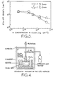
- the LEC technique is schematically indicated in Fig. 4.
- GaAs melt is coated with a liquid encapsulant (B203), and the GaAs crystal is pulled up under high pressure of 2-60 kg/cm 2 after the seed is attached to the melt.
- B203 liquid encapsulant
- This invention can also be carried out by employing a dopant other than boron, for example, aluminum.
- Both the Ga and As which were used as the starting materials were of the 6-nine grade (99.9999%) in purity.
- Two different B 2 0 3 encapsulants of the 5-nine grade (99.999%) which contained water of 300 ppm and 600 ppm were used.
- Boron shot (grains) having a diameter of 1 to 2 mm was used as the dopant.
- the primary boron-doped crystals were formed by direct synthesis method. Gallium, arsenic and boron were placed in a boron nitride crucible having a diameter of three inches, and B 2 0 3 was placed so as to cover the materials. They were melted by heating to about 800°C in the atmosphere of nitrogen gas having a pressure of 50 to 70 atms.
- the crystal was pulled up under the following conditions by the LEC method employing resistance heating, whereby a polycrystal body having a diameter of 38 mm was prepared (this diameter is not limitative, of course):
- the seed end containing particulate undissolved boron was removed from the polycrystalline body.
- the remaining polycrystalline body was crushed into small pieces measuring about 10 mm square, and these pieces were washed with aqua regia for about 10 minutes.
- the small pieces were remelted in the boron nitride crucible in the presence of B 2 O 3 (with boron if required), and the melt was pulled up in the ⁇ 1 0 0> direction under the following conditions by the LEC method employing resistance heating:
- the single crystal thus pulled up was 36 mm in diameter, 70 mm in length and 350 g in weight. These dimensions are not limitative, of course.
- Sample Nos. 1 to 5 The samples thus prepared are shown under Nos. 1 to 5 in TABLE 1.
- the single crystals were directly synthesized, and continuously pulled up at a pulling rate of from 3 to 20 mm.
- Sample Nos. 1 and 3 were both undoped, but prepared by employing B 2 0 3 encapsulants which differed in containing water of 600 ppm and 300 ppm, respectively.
- Sample No. 2 was doped with boron.
- Sample Nos. 4 and 5 were prepared by incorporating a large quantity of boron which is higher than 10 17 cm during direct synthesis, pulling polycrystals due to the presence of fine particles of undissolved boron, and then pulling single crystals from the polycrystals. Additional boron was incorporated for preparing Sample No. 5.
- TABLE 2 shows the results of SSMS (spark source mass spectrometric) analysis of Samples No. 1 to 5, and TABLE 3 shows the results of SSMS analysis of boron-doped polycrystals Nos. 40 and 50 from which Samples No. 4 and 5 were prepared, respectively.
- the concentration of boron in GaAs showed an increase in the range of 4.9x10 15 to 4.9x10 17 cm -3 , and such depended on the water content of B 2 0 3 used as the encapsulant, as the following reaction takes place:
- Sample No. 3 grown using B 2 0 3 having a water content of 300 ppm has a boron content which is 10 times higher than that of Sample No. 1 prepared by using B 2 0 3 having a water content of 600 ppm.
- Sample Nos. 40 and 50 showed a boron concentration which was as high as 1.6x10 18 cm- 3 , and a silicon concentration which was as low as 7.2x10 15 cm -3 .
- the middle-portion and tail end of the crystal showed a small variation in EPD. This was apparently due to the fact that the thermal stress was so high in the middle-portion and call end of the crystal that the quantity of boron incorporated was insufficient to achieve any substantial reduction in EPD.
- Resistivity and leakage current are important parameters for the evaluation of GaAs IC's, etc. Since the disordered crystal of a wafer surface can be ordered by annealing, the ion-implanted wafer must be annealed through IC's process. Sample Nos. 1 to 5 showed a resistivity of 5x10 6 to 5x10 8 ⁇ cm. This range of resistivity is quite satisfactory for GaAs IC's.
- the leakage current was measured in accordance with the two-probe method by applying a voltage of 1,000 V between the ends of the two probes under room light. The samples were examined for leakage current both before and after annealing which was performed for the capless wafers at 800°C for 30 minutes in a nitrogen gas atmosphere. The results are shown in TABLE 4.
Landscapes
- Chemical & Material Sciences (AREA)
- Engineering & Computer Science (AREA)
- Crystallography & Structural Chemistry (AREA)
- Materials Engineering (AREA)
- Metallurgy (AREA)
- Organic Chemistry (AREA)
- Inorganic Chemistry (AREA)
- Crystals, And After-Treatments Of Crystals (AREA)
- Liquid Deposition Of Substances Of Which Semiconductor Devices Are Composed (AREA)
Applications Claiming Priority (2)
| Application Number | Priority Date | Filing Date | Title |
|---|---|---|---|
| JP64508/82 | 1982-04-16 | ||
| JP57064508A JPS58181799A (ja) | 1982-04-16 | 1982-04-16 | 硼素を添加したGaAs単結晶の製造方法 |
Publications (2)
| Publication Number | Publication Date |
|---|---|
| EP0092409A1 true EP0092409A1 (fr) | 1983-10-26 |
| EP0092409B1 EP0092409B1 (fr) | 1986-07-30 |
Family
ID=13260205
Family Applications (1)
| Application Number | Title | Priority Date | Filing Date |
|---|---|---|---|
| EP83302165A Expired EP0092409B1 (fr) | 1982-04-16 | 1983-04-18 | Procédé de fabrication d'un monocristal d'arséniure de gallium dopé au bore |
Country Status (5)
| Country | Link |
|---|---|
| US (1) | US4528061A (fr) |
| EP (1) | EP0092409B1 (fr) |
| JP (1) | JPS58181799A (fr) |
| CA (1) | CA1212599A (fr) |
| DE (1) | DE3364873D1 (fr) |
Cited By (3)
| Publication number | Priority date | Publication date | Assignee | Title |
|---|---|---|---|---|
| FR2549500A1 (fr) * | 1983-07-20 | 1985-01-25 | Cominco Ltd | Procede de preparation de monocristaux semi-isolants de gaas |
| US4585511A (en) * | 1983-07-22 | 1986-04-29 | Cominco Ltd. | Method of growing gallium arsenide crystals using boron oxide encapsulant |
| US4697202A (en) * | 1984-02-02 | 1987-09-29 | Sri International | Integrated circuit having dislocation free substrate |
Families Citing this family (14)
| Publication number | Priority date | Publication date | Assignee | Title |
|---|---|---|---|---|
| JPS59232995A (ja) * | 1983-06-10 | 1984-12-27 | Sumitomo Electric Ind Ltd | 引上単結晶の冷却方法 |
| JP2529934B2 (ja) * | 1984-02-21 | 1996-09-04 | 住友電気工業株式会社 | 単結晶の製造方法 |
| JPS61222911A (ja) * | 1985-03-28 | 1986-10-03 | Toshiba Corp | 燐化化合物の合成方法 |
| JPS6270291A (ja) * | 1985-09-19 | 1987-03-31 | Toshiba Corp | GaAs単結晶の製造方法及び装置 |
| US4721539A (en) * | 1986-07-15 | 1988-01-26 | The United States Of America As Represented By The United States Department Of Energy | Large single crystal quaternary alloys of IB-IIIA-SE2 and methods of synthesizing the same |
| KR880009419A (ko) * | 1987-01-26 | 1988-09-15 | 이찌하라 시로 | 반도체소자의 제조방법 및 그 방법에 의해 제조된 반도체 소자 |
| US4923561A (en) * | 1988-09-23 | 1990-05-08 | American Telephone And Telegraph Company | Crystal growth method |
| US5186784A (en) * | 1989-06-20 | 1993-02-16 | Texas Instruments Incorporated | Process for improved doping of semiconductor crystals |
| US5431125A (en) * | 1991-06-14 | 1995-07-11 | The United States Of America As Represented By The Secretary Of The Air Force | Twin-free crystal growth of III-V semiconductor material |
| JP3015656B2 (ja) * | 1994-03-23 | 2000-03-06 | 株式会社東芝 | 半絶縁性GaAs単結晶の製造方法および製造装置 |
| JP4135239B2 (ja) * | 1997-12-26 | 2008-08-20 | 住友電気工業株式会社 | 半導体結晶およびその製造方法ならびに製造装置 |
| KR101266776B1 (ko) * | 2004-08-20 | 2013-05-28 | 미쓰비시 가가꾸 가부시키가이샤 | 금속 질화물 및 금속 질화물의 제조 방법 |
| JP2013026540A (ja) * | 2011-07-25 | 2013-02-04 | Renesas Electronics Corp | 半導体集積回路装置 |
| CN104900758B (zh) * | 2015-05-25 | 2017-03-15 | 连云港市产品质量监督检验中心 | 一种准单晶硅片微缺陷的检测方法 |
Family Cites Families (3)
| Publication number | Priority date | Publication date | Assignee | Title |
|---|---|---|---|---|
| DE2133875A1 (de) * | 1971-07-07 | 1973-01-18 | Siemens Ag | Verfahren zum ziehen von einkristallen, insbesondere fuer keimkristalle |
| JPS6028800B2 (ja) * | 1977-10-17 | 1985-07-06 | 住友電気工業株式会社 | 低欠陥密度りん化ガリウム単結晶 |
| US4200621A (en) * | 1978-07-18 | 1980-04-29 | Motorola, Inc. | Sequential purification and crystal growth |
-
1982
- 1982-04-16 JP JP57064508A patent/JPS58181799A/ja active Granted
-
1983
- 1983-04-15 CA CA000425974A patent/CA1212599A/fr not_active Expired
- 1983-04-15 US US06/485,355 patent/US4528061A/en not_active Expired - Lifetime
- 1983-04-18 DE DE8383302165T patent/DE3364873D1/de not_active Expired
- 1983-04-18 EP EP83302165A patent/EP0092409B1/fr not_active Expired
Non-Patent Citations (1)
| Title |
|---|
| SOLID STATE TECHNOLOGY, vol. 22, no. 1, January 1979, pages 59-67 * |
Cited By (4)
| Publication number | Priority date | Publication date | Assignee | Title |
|---|---|---|---|---|
| FR2549500A1 (fr) * | 1983-07-20 | 1985-01-25 | Cominco Ltd | Procede de preparation de monocristaux semi-isolants de gaas |
| DE3426250A1 (de) * | 1983-07-20 | 1985-01-31 | Cominco Ltd., Vancouver, British Columbia | Verfahren zur herstellung von halbisolierendem einkristall-gaas |
| US4585511A (en) * | 1983-07-22 | 1986-04-29 | Cominco Ltd. | Method of growing gallium arsenide crystals using boron oxide encapsulant |
| US4697202A (en) * | 1984-02-02 | 1987-09-29 | Sri International | Integrated circuit having dislocation free substrate |
Also Published As
| Publication number | Publication date |
|---|---|
| JPS58181799A (ja) | 1983-10-24 |
| CA1212599A (fr) | 1986-10-14 |
| EP0092409B1 (fr) | 1986-07-30 |
| US4528061A (en) | 1985-07-09 |
| JPS6129919B2 (fr) | 1986-07-10 |
| DE3364873D1 (en) | 1986-09-04 |
Similar Documents
| Publication | Publication Date | Title |
|---|---|---|
| EP0092409B1 (fr) | Procédé de fabrication d'un monocristal d'arséniure de gallium dopé au bore | |
| EP1634981B1 (fr) | Substrat de phosphure d'indium, cristal unique de phosphure d'indium et procede de fabrication correspondant | |
| US4478675A (en) | Method of producing GaAs single crystals doped with boron | |
| EP2607308A1 (fr) | Charge d'alimentation en silicium pour cellules solaires | |
| Nygren et al. | Properties of GaP single crystals grown by liquid encapsulated pulling | |
| WO2021251349A1 (fr) | Lingot de gaas, procédé de fabrication de lingot de gaas, et tranche de gaas | |
| Shinoyama et al. | Growth of dislocation-free undoped InP crystals | |
| US20090072205A1 (en) | Indium phosphide substrate, indium phosphide single crystal and process for producing them | |
| Deitch et al. | Bulk single crystal growth of silicon-germanium | |
| Cockayne et al. | The growth and perfection of single crystal indium phosphide produced by the LEC technique | |
| US6273969B1 (en) | Alloys and methods for their preparation | |
| Henry et al. | InP growth and properties | |
| Shinoyama et al. | Growth and crystal quality of InP crystals by the liquid encapsulated Czochralski technique | |
| Hemmat et al. | Closed System Vapor Growth of Bulk CdS Crystals from the Elemental Constituents | |
| Plaskett et al. | The Preparation and Properties of Large, Solution Grown GaP Crystals | |
| Iseler | Advances in LEC growth of InP crystals | |
| Ciszek | Synthesis and crystal growth of copper indium diselenide from the melt | |
| US4853077A (en) | Process for the preparation of mono-crystalline 3-5 semi-insulating materials by doping and use of the semi-insulating materials thus obtained | |
| Holmes et al. | Dislocation reduction in large-diameter LEC GaAs growth: I. Low gradient growth and indium doping | |
| EP4592431A1 (fr) | Procédé de production de lingot de gaas et lingot de gaas | |
| Reijnen et al. | Comparison Of LEC‐Grown And VGF‐Grown GaSb | |
| Kremer et al. | Low dislocation density GaAs grown by the vertical Bridgman technique | |
| JP2736343B2 (ja) | 半絶縁性InP単結晶の製造方法 | |
| RU2070233C1 (ru) | Способ получения объемных монокристаллов кремния р-типа | |
| JPH08756B2 (ja) | 無機化合物単結晶の成長方法 |
Legal Events
| Date | Code | Title | Description |
|---|---|---|---|
| PUAI | Public reference made under article 153(3) epc to a published international application that has entered the european phase |
Free format text: ORIGINAL CODE: 0009012 |
|
| AK | Designated contracting states |
Designated state(s): DE FR GB |
|
| 17P | Request for examination filed |
Effective date: 19840326 |
|
| RAP1 | Party data changed (applicant data changed or rights of an application transferred) |
Owner name: NIPPON TELEGRAPH AND TELEPHONE CORPORATION Owner name: SUMITOMO ELECTRIC INDUSTRIES LIMITED |
|
| GRAA | (expected) grant |
Free format text: ORIGINAL CODE: 0009210 |
|
| AK | Designated contracting states |
Kind code of ref document: B1 Designated state(s): DE FR GB |
|
| REF | Corresponds to: |
Ref document number: 3364873 Country of ref document: DE Date of ref document: 19860904 |
|
| ET | Fr: translation filed | ||
| PLBE | No opposition filed within time limit |
Free format text: ORIGINAL CODE: 0009261 |
|
| STAA | Information on the status of an ep patent application or granted ep patent |
Free format text: STATUS: NO OPPOSITION FILED WITHIN TIME LIMIT |
|
| 26N | No opposition filed | ||
| PGFP | Annual fee paid to national office [announced via postgrant information from national office to epo] |
Ref country code: FR Payment date: 20000411 Year of fee payment: 18 |
|
| PGFP | Annual fee paid to national office [announced via postgrant information from national office to epo] |
Ref country code: GB Payment date: 20000412 Year of fee payment: 18 |
|
| PGFP | Annual fee paid to national office [announced via postgrant information from national office to epo] |
Ref country code: DE Payment date: 20000417 Year of fee payment: 18 |
|
| PG25 | Lapsed in a contracting state [announced via postgrant information from national office to epo] |
Ref country code: GB Free format text: LAPSE BECAUSE OF NON-PAYMENT OF DUE FEES Effective date: 20010418 |
|
| PG25 | Lapsed in a contracting state [announced via postgrant information from national office to epo] |
Ref country code: FR Free format text: THE PATENT HAS BEEN ANNULLED BY A DECISION OF A NATIONAL AUTHORITY Effective date: 20010430 |
|
| GBPC | Gb: european patent ceased through non-payment of renewal fee |
Effective date: 20010418 |
|
| PG25 | Lapsed in a contracting state [announced via postgrant information from national office to epo] |
Ref country code: DE Free format text: LAPSE BECAUSE OF NON-PAYMENT OF DUE FEES Effective date: 20020201 |
|
| REG | Reference to a national code |
Ref country code: FR Ref legal event code: ST |